MIPI CSI
18.1 Introduction
MIPI CSI (Camera Serial Interface) is a specification defined by MIPI (Mobile Industry Processor Interface) for connecting a camera and a CPU to transmit video signals from a camera. SP7021 supports CSI-2 specification which was released in 2005, using D-PHY as the physical layer. The main features list as below.
...
SP7021 supports two MIPI CSI-RX modules, the control registers locate at RGST Table Group 165~168 which memory map address are 9c005280h~9c00547fh.
Although the below descriptions focus on MIPI CSI0 module, but the MIPI CSI1 has the same structure.
18.2 Function Diagram
18.2.1 MIPI CSI connection
Figure 18-1 shows the generic MIPI CSI pins connection.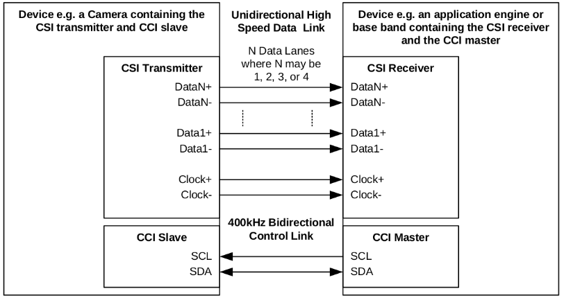
Figure 18-1 MIPI CSI Connection
- CCI (Camera Control Interface) is a two-way connection and is compatible with the I2C protocol. This interface is mainly used to access the registers in the camera to configure and control them. The host's I2C host controller is usually used, and the camera is used as the I2C slave device. The camera register layout and field definitions of different manufacturers are different.
- The CSI interface is a one-way transmission, which consists of a clock lane and one to four data lanes to transmit image data. Adopt D-PHY physical layer protocol.
18.2.2 MIPI CSI RX Block
A generalized function diagram of MIPI CSI of SP7021 is shown in Figure 18-2.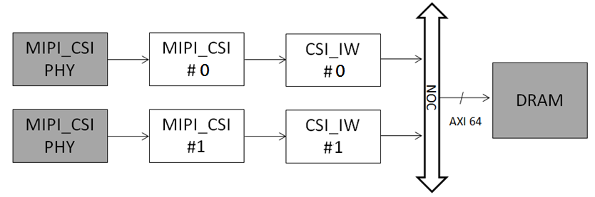
Figure 18-2 MIPI CSI Functional Blocks
- MIPI-CSI PHY: The DPHY supports forward direction HS/LP transaction and reverse direction LP transaction.
- MIPI-CSI: MIPI-CSI receive data from DPHY and decode data (unpacks formats and byte to pixel).
- CSI-IW: Receive data from MIPI-CSI and store into DRAM.
18.3 DPHY Protocol
Figure 18-3 shows the data transfer behavior between DPHYTX and DPHYRX which is described in DPHY SPEC.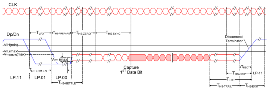
Figure 18-3 DPHY Protocol
In the part where the DP/DN is blue, it belongs to Low Power Mode, and the behavior on the interface is Large Voltage Swing. The part where the DP/DN is red line belongs to High Speed Mode, and the behavior on the interface is Low Voltage Swing. When you want to start transferring data, you will enter High Speed Mode from Low Power Mode. The behaviors will be in Low Power Mode with the voltage change from LP-11 -> LP-01 -> LP-00. After entering High Speed Mode, a series of HS-0 will be transmitted as the buffer between conversions. The followed HS-Sync pattern with data transmission is the valid data transmission
18.4 DPHY Operation with MIPI CSI
To start the entire MIPI System, firstly open the DPHY Low Power Mode Enable bit to transmit the lane (G165.6 mipi_analog_cfg2 register bit4). MIPI CSI will use Power Status Signal to determine when to enter High Speed Mode (basically by 1->0). Once you want to enter High Speed Mode, it will delay for a period of time (such as T-HS-SETTLE in Figure 18-2, controlled by G165.9 mipicsi_delay_ctl register bit[15:8]) and then pull up HS Mode Enable to notify DPHY. On the other hand, if you enter Low Power Mode, MIPI CSI will lower HS Mode Enable.
When data transmission is performed on the data lane, the HS-SETTLE and HS-SYNC signals are sent first, then the data payload is sent, and finally ends with EOT (end of transmission), which is a complete physical layer packet.
18.5 MIPI CSI Protocol
The MIPI CSI protocol include 3 layers, they are Pixel/Byte with Packing/Unpacking layer, Low Level Protocol layer and Lane Management layer. The protocol structure shows in figure 18-4.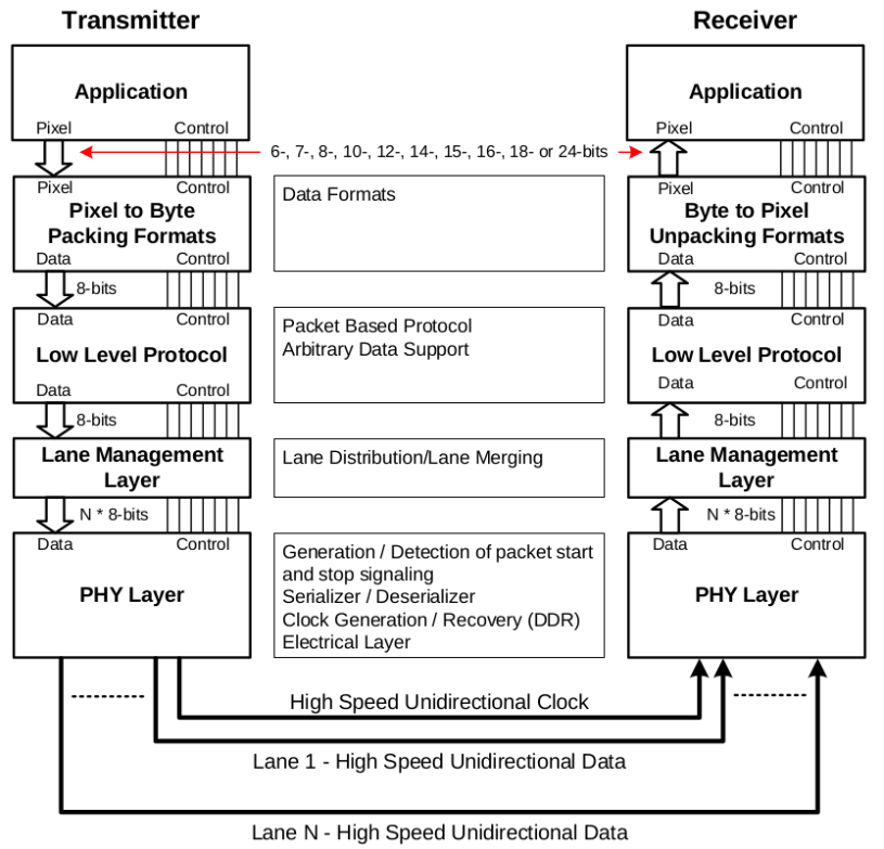
Figure 18-4 MIPI CSI Protocol
18.5.1 Pixel/Byte with Packing/Unpacking Layer
In this layer, the transmitting end receives the pixel data from the application layer and packages it into a byte format for transmission to the next layer; at the receiving end, unpacks the data from the LLP (Low Level Protocol) layer and transmits it to the application layer.The main purpose of this layer is to convert different pixel formats (such as YUYV, RGBA, etc.) into 8-bit format, eliminating differences in different image formats and reducing transmission complexity.
18.5.2 Low Level Protocol Layer
The Low Level Protocol (LLP) layer is the main functional layer of the CSI protocol. It not only defines the packet format, but also defines the synchronization mechanism used in the transmission.
At the transmitting end, the layer is responsible for packing the data transmitted from the upper layer, adding a check field, adding the synchronization packet, and transmitting to the next layer; At the receiving end, the integrity of the packet is first verified, and each field is parsed, and the corresponding operation is performed according to the packet type, and the image data is transmitted to the upper layer.
The LLP processed payload data is converted pure byte data, and there is no pixel concept. The transmission of image data of one frame and one frame is realized by defining different fields and packet types.
18.5.3 Lane Management Layer
MIPI CSI-2 can be extended with data lane based on performance requirements. The number of data lanes can be one, two, three or four for different bandwidth requirements. The sender automatically distributes the data to each lane for transmission according to the number of lanes used; at the receiving end, the data on each lane is re-merged to recover the data.
This layer treats the packet transmitted by the LLP as a piece of pure byte data, and distributes it according to the number of lanes, regardless of the meaning of the data in the packet.
18.6 Registers Map
| Anchor | ||||
|---|---|---|---|---|
|
RGST Table Group 165 MIPI CSI DePacket : MIPICSI0
165.0 MIPICSI key signal status (mipicsi status)
Address:0x9C005280
Reset:0x0
| Field |
...
| Name | Bit | Access | Description |
| reserved | 31:3 | RO | Reserved |
| SOL FLAG |
...
| 2 | W1C | Receive MIPI SOL (Start of line) The Condition is a. : SOT flag and |
...
| b. : Receive DI of long packet |
| SOF FLAG |
...
| 1 | W1C | Receive MIPI SOF (Start of frame) The Condition is a. : SOT flag and b. : Receive DI of frame start short packet | |
| SOT FLAG |
...
| 0 | W1C | Receive MIPI SOT (Start of transmission) The Condition is a. : DPHY power status from LP to HS and b. : Receive HS Sync-Sequence |
165.1 MIPICSI debug 0 (mipi debug0)
Address: 0x9C005284
Reset:
...
0x9C005284
0x0
...
...
...
0x0
Field Name |
| Bit | Access | Descriptionreserved reserved |
| reserved |
| 31:10 | RO | Reserved |
| reserved | 9:4 | RO | Reserved | |
reserved | 3:0 | RO RW RO | Reserved Reserved Reserved |
165.2 MIPICSI word count and analog LPF (mipi wc lpf)
Address: 0x9C005288
Reset: 0x0
| Field |
...
| Name | Bit | Access | Description |
| reserved | 31:19 | RO | Reserved |
| LPF |
...
| RX | 18:16 | RW | Analog Control : LPF Bandwidth Control LP State of MIPI mode 3'bx00 to 3'bx11 (Bandwidth decreasing) Default Value = 3'bx00 |
| WORD COUNT | 15: |
...
| 0 | RO | Word count value from PH |
165.3 MIPICSI analog config register 0 (mipi analog cfg0)
Address: 0x9C00528C
Reset: 0x00000015
| Field |
...
| Name | Bit | Access | Description |
| reserved | 31: |
...
| 7 | RO | Reserve | |
CEN | 6:4 | RW | Tail current control of OP in D2S |
PHY TEST | 3:0 | RW | Bias current control |
165.4 MIPICSI analog config register 1 (mipi analog cfg1)
Address: 0x9C005290
Reset:
...
0x9C005290
0x0000 0000
...
...
...
0x0000 0000
Field Name |
| Bit | Access | Description |
reserved |
| 31:13 | RO | Reserved |
|
|
|
|
|
reserved | 11:9 | RO | Reserved | |
|
|
|
|
|
|
|
|
| |
|
|
|
|
...
165.5 MIPICSI FSM reset (mipicsi fsm rst)
Address: 0x9C005294
Reset: 0x0000 0001
| Field |
...
| Name | Bit | Access | Description |
| reserved | 31:1 | RO | Reserved |
| FSM |
...
| RST | 0 | RW | Reset control FSM enable 0: Disable 1: Enable (Default) |
165.6 MIPICSI analog config register 2 (mipi analog cfg2)
Address: 0x9C005298
Reset: 0x0000 0000
| Field |
...
| Name | Bit | Access | Description |
| reserved | 31:5 | RO | Reserved |
| ENLP CLK LANE | 4 | RW | Enable clock lane of LP mode circuit 0 : Power Down 1 : Normal Mode (Default) |
| ENLP DATA LANE | 3:0 | RW | Enable data lane of LP mode circuit EN DATA LANE[0] : Data Lane 0 EN DATA LANE[1] : Data Lane 1 EN DATA LANE[2] : Data Lane 2 EN DATA LANE[3] : Data Lane 3 Data lane enable signal 0 : Power Down 1 : Normal Mode Default = 4'b1111 |
165.7 Enable MIPICSI (mipicsi enable)
Address: 0x9C00529C
Reset: 0x0000 0001
| Field |
...
| Name | Bit | Access | Description |
reserved | 31:1 | RO | Reserved |
MIPICSI ENABLE | 0 | RW | Enable MIPICSI |
165.8 MIPICSI digital and analog config register (mipicsi mix cfg)
Address: 0x9C0052A0
Reset: 0x0001 8100
| Field |
...
| Name | Bit | Access | Description |
| reserved | 31:22 | RO | Reserved |
| LANE NUM | 21:20 | RW | MIPI input lane number 0x0 : 1 Lane (Default) 0x1 : 2 Lane Others : 4 Lane |
...
| reserved | 19 | RO | Reserved |
| DEC MODE | 18:16 |
...
| MIPI input data format 0x1 : Raw 10 (Default) 0x2 : Raw 8 Others : No Support | ||
| EOF METHOD |
...
| SEL | 15 | RW | Output EOF generation method 0 : When receive the number of the VTOTAL line to gener- ate eol 1 : When detect eof control word to generate eof (Default) Fix 1 for Q628 CSIIW |
| LINE CNT |
...
| SEL | 14 | RW | Line count increase method 0 : When SOL detected (Default) 1 : When EOL detected Fix 0 for Q628 CSIIW |
| EOL METHOD |
...
| SEL | 13 | RW | Output EOL generation method 0 : When receive the number of the word count data to generate eol (Default) 1 : When detect eol control word to generate eol Fix 0 for Q628 CSIIW |
WORDCNT SEL | 12 | RW | Auto or manual generate word number selection |
reserved | 11:9 | RO | Reserved |
|
|
|
|
reserved | 7:6 | RO | Reserved |
|
|
|
|
|
|
|
|
|
|
|
|
No USED CFG0 | 1:0 | RW | No used control. Fix to 2'b00 |
165.9 Signal delay setting (mipicsi delay ctl)
Address: 0x9C0052A4
Reset:
...
0x0003 0400
|
|
| Field Name |
| Bit | Access | Description |
reserved |
| 31:24 | RO | Reserved | |||
|
|
|
|
| |||
|
|
|
| ||||
reserved |
| 7:0 | RO | Reserved |
165.10 Long packet size and number config (mipicsi packet size)
Address: 0x9C0052A8
Reset: 0x0
| Field |
...
| Name | Bit | Access | Description |
| reserved | 31:28 | RO | Reserved |
| VTOTAL | 27:16 | RW | Long packet number setting Note : Only valid when set WORDCNT SEL = 1. |
...
| reserved | 15:13 | RO | Reserved |
| HTOTAL | 12:0 | RW | Long packet size setting Note : Only valid when set WORDCNT SEL = 1. |
165.11SOT11 SOT sync word (mipicsi sot syncword)
Address: 0x9C0052AC
Reset: 0x0000 00B8
| Field |
...
| Name | Bit | Access | Description |
| reserved | 31:16 | RO | Reserved |
| SOT |
...
| SYNCWORD | 15:0 | RW | MIPI SPEC default value 0xB8 |
165.12 SOF, SOL sync word (mipicsi sof sol syncword)
Address: 0x9C0052B0
Reset: 0x0
| Field |
...
| Name | Bit | Access | Description |
| SOF |
...
| SYNCWORD | 31:16 | RW | MIPI SPEC default value 0x0 |
| SOL |
...
| SYNCWORD | 15:0 | RW | According to different input data foramt or LS short packet (DI Value) |
165.13 EOF, EOL sync word (mipicsi eof eol syncword)
Address: 0x9C0052B4
Reset: 0x0001 0000
| Field |
...
| Name | Bit | Access | Description |
| EOF |
...
| SYNCWORD | 31:16 | RW | MIPI SPEC default value 0x1 |
| EOL |
...
| SYNCWORD | 15:0 | RW | According to LE short packet DI value |
165.14 Reserved (mipicsi reserved a14)
Address: 0x9C0052B8
Reset: 0x0
| Field |
...
| Name | Bit | Access | Description |
| reserved | 31:0 | RO | Reserved |
165.15 Reserved (mipicsi reserved a15)
Address: 0x9C0052BC
Reset: 0x0
| Field |
...
| Name | Bit | Access | Description |
| reserved | 31:0 | RO | Reserved |
165.16 ECC error status (mipicsi ecc error)
Address: 0x9C0052C0
Reset: 0x0
| Field |
...
| Name | Bit | Access | Description |
| reserved | 31:3 | RO | Reserved |
| ECC 2BIT |
...
| ERROR | 2 | W1C | Indicate ecc 2 bit error |
| ECC 1BIT |
...
| ERROR | 1 | W1C | Indicate ecc 1 bit error |
...
| CTRLWORD ERROR | 0 | W1C | Indicate control word error |
165.17CRC17 CRC error status (mipicsi crc error)
Address: 0x9C0052C4
Reset:
...
0x9C0052C4
0x0
...
...
...
0x0
| Field Name |
| Bit | Access | Description |
|
| reserved | 31:1 | RO | Reserved | ||
| CRC ERROR | 0 | W1C | Indicate crc error |
165.18 ECC config (mipicsi ecc cfg)
...
...
...
...
...
Address: 0x9C0052C8
Reset:
...
...
...
...
0x0000 0010
Field Name |
| Bit | Access | Description |
|
reserved |
| 31:9 | RO | Reserved | |
|
|
|
| ||
|
|
|
|
| |
|
|
|
|
| |
|
|
|
| ||
|
|
|
|
|
165.19 MIPICSI analog config register 3 (mipi analog cfg3)
Address: 0x9C0052CC
Reset: 0x0
| Field |
...
| Name | Bit | Access | Description |
PHCALDA | 31:8 | RW | Polarity and delay adjustment of clock lane |
reserved | 7:6 | RO | Reserved |
|
|
|
|
165.20 MIPICSI analog config register 4 (mipi analog cfg4)
Address: 0x9C0052D0
Reset: 0x0
| Field |
...
| Name | Bit | Access | Description |
| reserved | 31:16 | RO | Reserved |
| PHY |
...
| REV | 15:0 | RW | PHY Reserved |
RGST Table Group 166 MIPI CSI Image Write : CSIIW0
166.0CSIIW0 CSIIW latch mode (csiiw latch mode)
Address: 0x9C005300
Reset: 0x0
| Field |
...
| Name | Bit | Access | Description |
| reserved | 31:1 | RO | Reserved |
| LATCH EN | 0 | RW | Latch mode enable 0: Direct Mode (Default) 1: Latch Mode |
166.1CSIIW1 CSIIW config register 0 (csiiw config0)
Address: 0x9C005304
Reset: 0x0000 2700
Field NameBitAccessDescription
| reserved |
...
| 31:18 | RO | Reserved |
| IRQ MASK |
...
| FE | 17 | RW | Frame end IRQ mask 0: Disable (default) 1: Enable |
| IRQ MASK |
...
| FS | 16 | RW | Frame start IRQ mask 0: Disable (default) 1: Enable |
| CMD URGENT TH | 15:12 | RW | Bus urgent command threadshold Set 0 to stop urgent signal Set 8 to always send urgent signal Set 9-15 equal to 8 (Mean noused) |
| reserved | 11 | RO |
...
| Reserved |
| CMD |
...
| QUEUE | 10:8 | RW | Bus command queue for rate control Set 0 to stop bus handshark |
| reserved | 7: |
...
| 6 | RO | Reserved | |
DES DATA 2BYTE | 5 | RW | Write data to DRAM with 2 byte per pixel |
SRC DATA MODE | 4 | RW | Source data format |
reserved | 3:1 | RO | Reserved |
|
|
|
|
166.2CSIIW2 CSIIW base address (csiiw base addr)
Address: 0x9C005308
Reset: 0x0
Field Name | Bit | Access | Description |
BASE ADDR | 31:8 | RW | Base address setting |
reserved | 7:0 | RO | Reserved |
166.3CSIIW3 CSIIW line stride (csiiw stride)
Address: 0x9C00530C
Reset: 0x0
| Field |
...
| Name | Bit | Access | Description |
| reserved | 31:14 | RO | Reserved |
| LINE |
...
| STRIDE | 13:4 | RW | Line stride |
...
| setting Unit : 16 bytes |
...
| reserved | 3:0 | RO | Reserved |
166.4CSIIW4 CSIIW frame size (csiiw frame size)
Address: 0x9C005310
Reset: 0x8000 0000
| Field |
...
| Name | Bit | Access | Description |
| SZIE AUTO EN | 31 | RW | Frame size automatic detect after receiving 3 frames 0: Disable (default) 1: Enable |
| reserved | 30: |
...
| 28 | RO | Reserved | |
| YLEN | 27:16 | RW | Vertical frame size Unit : Line Mod 2 equal |
...
| 0 | |||
| reserved | 15:13 | RO | Reserved |
| XLEN | 12:0 | RW |
...
| orizontal frame size Unit : Pixel 8 bits source :Mod 2 equal 0 10 bits source : Mod 4 equal 0 |
166.5CSIIW5 CSIIW frame buffer rorate (csiiw frmae buf)
Address: 0x9C005314
Reset: 0x0
| Field |
...
| Name | Bit | Access | Description |
| reserved | 31:29 | RO | Reserved |
| BUF ROTATE |
...
| DEBUG | 28 | RW | Frame buffer only rorate one cycle Debug used |
...
| reserved | 27 | RO | Reserved |
| BUF ROTATE NUM | 26:24 | RW | Number of frame buffer automatic rotation Set 0 to stop automatic rotation function |
| ADDR |
...
| OFFSET | 23:8 | RW | Base address offset for frame buffer rotate automatic Unit : 256 bytes |
...
| reserved | 7:0 | RO | Reserved |
166.6CSIIW6 CSIIW config register 1 (csiiw config1)
Address:0x9C005318
Reset:0x0
Field NameBitAccessDescription
reserved31:1RO : 0x9C005318
Reset: 0x0
| Field Name | Bit | Access | Description |
| reserved | 31:1 | RO | Reserved |
| DECIMATION EN | 0 | RW | Source data vertical and horizontal decimation Note : Horizontal and vertical sizes both need mod 4 equal 0 0: Disable (default) 1: Enable |
166.7CSIIW7 CSIIW frame size of HW automatic detection (csiiw frame size ro)
Address: 0x9C00531C
Reset: 0x0
| Field |
...
| Name | Bit | Access | Description |
| reserved | 31:28 | RO | Reserved |
| RO YLEN | 27: |
...
| 16 | RW | Vertical frame size of HW automatic detection Unit : Line |
...
| reserved | 15:13 | RO | Reserved |
| RO XLEN | 12: |
...
| 0 | RW | Horizontal frame size of HW automatic detection Unit : Pixel |
RGST Table Group 167 MIPI CSI DePacket : MIPICSI1
167.0 MIPICSI key signal status (mipicsi status)
Address: 0x9C005380
Reset: 0x0
| Field |
...
| Name | Bit | Access | Description |
| reserved | 31:3 | RO | Reserved |
| SOL FLAG | 2 | W1C | Receive MIPI SOL (Start of line) The Condition is a. : SOT flag and b. : Receive DI of long packet |
| SOF FLAG |
...
| 1 | W1C | Receive MIPI SOF (Start of frame) The Condition is a. : SOT flag and b. : Receive DI of frame start short packet | |
| SOT FLAG |
...
| 0 | W1C | Receive MIPI SOT (Start of transmission) The Condition is a. : DPHY power status from LP to HS and b. : Receive HS Sync-Sequence |
167.1 MIPICSI debug 0 (mipi debug0)
Address: 0x9C005384
Reset: 0x0
| Field Name | Bit | Access | Description |
| reserved | 31:10 | RO | Reserved |
| reserved | 9:4 |
...
| RO | Reserved | ||
| reserved | 3:0 | RO | Reserved |
167.2 MIPICSI word count and analog LPF (mipi wc lpf)
Address: 0x9C005388
Reset: 0x0
| Field |
...
| Name | Bit | Access | Description |
| reserved | 31:19 | RO | Reserved |
| LPF |
...
| RX | 18:16 | RW | Analog Control : LPF Bandwidth Control LP State of MIPI mode 3'bx00 to 3'bx11 (Bandwidth decreasing) Default Value = 3'bx00 |
| WORD COUNT | 15: |
...
| 0 | RO | Word count value from PH |
167.3 MIPICSI analog config register 0 (mipi analog cfg0)
Address: 0x9C00538C
Reset: 0x0000 0015
| Field |
...
| Name | Bit | Access | Description |
| reserved | 31:7 | RO | Reserved |
| CEN | 6:4 | RW | Tail current control of OP in D2S 0x0 : 18*Ibias 0x1 : 22*Ibias (Default) 0x2 : 26*Ibias 0x3 : 30*Ibias |
| PHY |
...
| TEST | 3:0 | RW | Bias current control 0x0 : 5uA 0x1 : 10uA 0x2 : 15uA 0x3 : 20uA 0x4 : 25uA 0x5 : 30uA (Default) 0x6 : 35uA 0x7 : 40uA |
167.4 MIPICSI analog config register 1 (mipi analog cfg1)
Address: 0x9C005390
Reset:
...
0x0000 0000
|
|
| Field Name |
| Bit | Access | Description |
reserved | 31:13 | RO | Reserved | ||||
|
|
|
| ||||
reserved | 11:9 | RO | Reserved | ||||
|
|
|
|
| |||
|
|
|
|
| |||
|
|
|
|
|
167.5 MIPICSI FSM reset (mipicsi fsm rst)
Address: 0x9C005394
Reset: 0x0000 0001
| Field |
...
| Name | Bit | Access | Description |
| reserved | 31:1 | RO | Reserved |
| FSM |
...
| RST | 0 | RW | Reset control FSM enable 0: Disable 1: Enable (Default) |
167.6 MIPICSI analog config register 2 (mipi analog cfg2)
Address: 0x9C005398
Reset: 0x0000 0000
...
167.7 Enable MIPICSI (mipicsi enable)
Address: 0x9C00539C
Reset: 0x0000 0001
...
...
| Field Name | Bit | Access | Description |
reserved | 31:1 | RO | Reserved | |
|
|
|
|
167.8 MIPICSI digital and analog config register (mipicsi mix cfg)
Address:0x9C0053A0
Reset: 0x0001 8100
Field NameBitAccessDescription
reserved31:22RO : 0x9C0053A0
Reset: 0x0001 8100
| Field Name | Bit | Access | Description |
| reserved | 31:22 | RO | Reserved |
LANE NUM | 21:20 | RW | MIPI input lane number |
reserved | 19 | RO | Reserved |
|
|
|
|
EOF METHOD SEL | 15 | RW | Output EOF generation method |
LINE CNT SEL | 14 | RW | Line count increase method |
EOL METHOD SEL | 13 | RW | Output EOL generation method |
WORDCNT SEL | 12 | RW | Auto or manual generate word number selection |
reserved | 11:9 | RO | Reserved |
|
|
|
|
reserved | 7:6 | RO | Reserved |
|
|
|
|
|
|
|
|
|
|
|
|
| No USED |
...
| CFG0 | 1:0 | RW | No used control. Fix to 2'b00 |
167.9 Signal delay setting (mipicsi delay ctl)
Address: 0x9C0053A4
Reset:
...
0x0003 0400
|
|
| Field Name |
| Bit | Access | Description |
reserved | 31:24 | RO | Reserved | ||||
|
|
|
| ||||
|
|
|
|
| |||
reserved | 7:0 | RO | Reserved |
167.10 Long packet size and number config (mipicsi packet size)
Address: 0x9C0053A8
Reset:
...
0x9C0053A8
0x0
...
...
...
0x0
Field Name | Bit | Access | Description | |
reserved | 31:28 | RO | Reserved | |
|
|
|
|
|
reserved | 15:13 | RO | Reserved | |
|
|
|
|
167.11SOT11 SOT sync word (mipicsi sot syncword)
Address: 0x9C0053AC
Reset: 0x0000 00B8
Field NameBitAccessDescription
reserved31:16RO
| Field Name | Bit | Access | Description |
| reserved | 31:16 | RO | Reserved |
| SOT |
...
| SYNCWORD | 15:0 | RW | MIPI SPEC default value 0xB8 |
167.12 SOF, SOL sync word (mipicsi sof sol syncword)
Address: 0x9C0053B0
Reset: 0x0
| Field |
...
| Name | Bit | Access | Description |
| SOF |
...
| SYNCWORD | 31:16 | RW | MIPI SPEC default value 0x0 |
| SOL |
...
| SYNCWORD | 15:0 | RW | According to different input data foramt or LS short packet (DI Value) |
167.13 EOF, EOL sync word (mipicsi eof eol syncword)
Address: 0x9C0053B4
Reset: 0x0001 0000
| Field |
...
| Name | Bit | Access | Description |
| EOF |
...
| SYNCWORD | 31:16 | RW | MIPI SPEC default value 0x1 |
| EOL |
...
| SYNCWORD | 15:0 | RW | According to LE short packet DI value |
167.14 Reserved (mipicsi reserved a14)
Address: 0x9C0053B8
Reset: 0x0
| Field |
...
| Name | Bit | Access | Description |
| reserved | 31:0 | RO | Reserved |
167.15 Reserved (mipicsi reserved a15)
Address: 0x9C0053BC Reset: 0x0
| Field |
...
| Name | Bit | Access | Description |
| reserved | 31:0 | RO | Reserved |
167.16 ECC error status (mipicsi ecc error)
Address: 0x9C0053C0
Reset:0x0
|
|
|
| Field Name |
| Bit | Access | Description |
reserved |
| 31:4 | RO | Reserved | ||||
|
|
|
| |||||
|
|
|
|
|
| |||
|
|
|
|
|
|
167.
...
17 CRC error status (mipicsi crc error)
...
...
...
...
...
Address: 0x9C0053C4
Reset:
...
0x9C0053C4
0x0
...
...
...
...
0x0
| Field Name | Bit | Access | Description | ||
| reserved | 31:1 | RO | Reserved |
| |
| CRC ERROR |
| 0 | W1C | Indicate crc error |
|
167.18 ECC config (mipicsi ecc cfg)
Address: 0x9C0053C8
Reset: 0x0000 0010
Field Name | Bit | Access | Description |
reserved | 31:9 | RO | Reserved |
|
|
|
|
|
|
|
|
|
|
|
|
|
|
|
|
|
|
|
|
167.19 MIPICSI analog config register 3 (mipi analog cfg3)
Address: 0x9C0053CC
Reset: 0x0
| Field |
...
| Name | Bit | Access | Description |
| PHCALDA | 31:8 | RW | Polarity and delay adjustment of clock lane PHCALDA[5:0] : Data Lane 0 PHCALDA[11:6] : Data Lane 1 PHCALDA[17:12] : Data Lane 2 PHCALDA[23:18] : Data Lane 3 PHCALDA[5] : Polarity Control 1'b0 : Normal Polarity 1'b1 : Inverse Polarity PHCALDA[4:0] : 0x0-0xF 0 ps - 527 ps, Step : 17 ps |
...
| reserved | 7:6 | RO | Reserved |
| PHCALCK | 5:0 | RW | Polarity and delay adjustment of clock lane PHCALCK[5] : Polarity Control 1'b0 :NormalPolarity 1'b1 : Inverse Polarity PHCALCK[4:0] : 0x0-0xF 0 ps - 527 ps, Step : 17 p |
167.20 MIPICSI analog config register 4 (mipi analog cfg4)
Address: 0x9C0053D0
Reset: 0x0
| Field |
...
| Name | Bit | Access | Description |
| reserved | 31:16 | RO | Reserved |
| PHY |
...
| REV | 15:0 | RW | PHY Reserved |
RGST Table Group 168 MIPI CSI Image Write : CSIIW1
168.0CSIIW0 CSIIW latch mode (csiiw latch mode)
Address: 0x9C005400
Reset: 0x0
| Field |
...
| Name | Bit | Access | Description |
| reserved | 31:1 | RO | Reserved |
| LATCH EN | 0 | RW | Latch mode enable 0: Direct Mode (Default) 1: Latch Mode |
168.1CSIIW1 CSIIW config register 0 (csiiw config0)
Address:0x9C005404
Reset: 0x0000 2700
Field NameBitAccessDescription
reserved31:18RO )
Address: 0x9C005404
Reset: 0x0000 2700
| Field Name | Bit | Access | Description |
| reserved | 31:18 | RO | Reserved |
| IRQ MASK |
...
| FE | 17 | RW | Frame end IRQ mask 0: Disable (default) 1: Enable |
| IRQ MASK |
...
| FS | 16 | RW | Frame start IRQ mask 0: Disable (default) 1: Enable |
| CMD URGENT TH | 15:12 | RW | Bus urgent command threadshold Set 0 to stop urgent signal Set 8 to always send urgent signal Set 9-15 equal to 8 (Mean noused) |
...
| reserved | 11 | RO | Reserved |
| CMD |
...
| QUEUE | 10:8 |
...
| Bus command queue for rate control |
...
| reserved | 7: |
...
| 6 | RO | Reserved | |
DES DATA 2BYTE | 5 | RW | Write data to DRAM with 2 byte per pixel |
SRC DATA MODE | 4 | RW | Source data format |
reserved | 3:1 | RO | Reserved |
|
|
|
|
168.2CSIIW2 CSIIW base address (csiiw base addr)
Address: 0x9C005408
Reset: 0x0
Field Name | Bit | Access | Description |
BASE ADDR | 31:8 | RW | Base address setting |
reserved | 7:0 | RO | Reserved |
168.3CSIIW3 CSIIW line stride (csiiw stride)
Address: 0x9C00540C
Reset: 0x0
| Field |
...
| Name | Bit | Access | Description |
| reserved | 31:14 | RO | Reserved |
| LINE |
...
| STRIDE | 13:4 | RW | Line stride setting Unit : 16 bytes |
...
| reserved | 3:0 | RO | Reserved |
168.4CSIIW4 CSIIW frame size (csiiw frame size)
Address: 0x9C005410
Reset: 0x8000 0000
| Field |
...
| Name | Bit | Access | Description |
| SZIE AUTO EN | 31 | RW | Frame size automatic detect after receiving 3 frames 0: Disable (default) 1: Enable |
| reserved | 30: |
...
| 28 | RO | Reserved | |
| YLEN | 27:16 | RW | Vertical frame size Unit : Line Mod 2 equal 0 |
...
| reserved | 15:13 | RO | Reserved |
| XLEN | 12:0 | RW | Horizontal frame size Unit : Pixel 8 bits source :Mod 2 equal 0 10 bits source : Mod 4 equal 0 |
168.5CSIIW5 CSIIW frame buffer rorate (csiiw frmae buf)
Address: 0x9C005414
Reset: 0x0
| Field |
...
| Name | Bit | Access | Description |
| reserved | 31:29 | RO | Reserved |
| BUF ROTATE |
...
| DEBUG | 28 | RW | Frame buffer only rorate one cycle Debug used |
...
| reserved | 27 | RO | Reserved |
| BUF ROTATE NUM | 26:24 | RW | Number of frame buffer automatic rotation Set 0 to stop automatic rotation function |
| ADDR |
...
| OFFSET | 23:8 | RW | Base address offset for frame buffer rotate automatic Unit : 256 bytes |
...
| reserved | 7:0 | RO | Reserved |
168.6CSIIW6 CSIIW config register 1 (csiiw config1)
Address: 0x9C005418
Reset: 0x0
| Field |
...
| Name | Bit | Access | Description |
| reserved | 31:1 | RO | Reserved |
| DECIMATION EN | 0 | RW | Source data vertical and horizontal decimation Note : Horizontal and vertical sizes both need mod 4 equal 0 0: Disable (default) 1: Enable |
168.7CSIIW7 CSIIW frame size of HW automatic detection (csiiw frame size ro)
Address: 0x9C00541C
Reset: 0x0
| Field |
...
| Name | Bit | Access | Description |
| reserved | 31:28 | RO | Reserved |
| RO YLEN | 27: |
...
| 16 | RW | Vertical frame size of HW automatic detection Unit : Line |
...
| reserved | 15:13 | RO | Reserved |
| RO XLEN | 12: |
...
| 0 | RW | Horizontal frame size of HW automatic detection Unit : Pixel |