...
Group101.25~31 (abbreviation as G101.25~31) registers are used for set GPIO_FIRST (for pad control, “1” means GPIO, “0” means Multiplex function ) state. Each bit map to one pin. For example, G101.25[0] control GPIO_P0_00 pin’s GPIO_FIRST state.
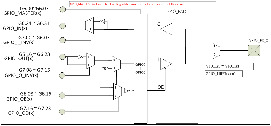
Figure 4.5-1 GPIO Block Diagram
5.3.1. Set General Purpose I/O Pin Method
...
Please notice that user should prevent set several signals in the same pin, one signal only can be assign to one pin.
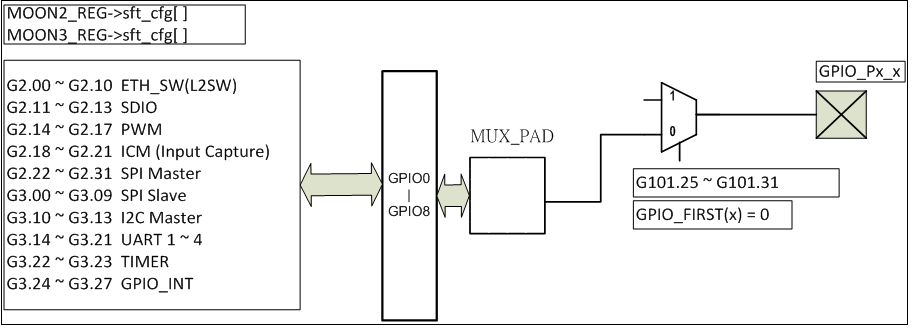
Figure 5.-2 Multiplex Peripheral Pin Block Diagram
5.4.1. Set Multiplex Peripheral Pin Method
...