...
The SP7021 utilizes system in package (SIP) technology to provide an internal buffer SDARM within the package. The SP7021 supports 1Gb and 4Gb of internal SDRAMs. The SDRAM is DDR3 (Double Data Rate 3) 1066max type and uses a 16-bit data interface. 16-bit and 8-bit data interfaces are both supported. It supports DFI2.1 to DRAM controller with DFI and PHY clock ratio is 1:2 and 1:1. The DRAM memory map area locates at address 0x00000000~0x1FFFFFFF which have 512MB size. The control registers address locates at 0x9C001900~0x9C001AFF.
15.2 Function Diagram
The SP7021 DRAM controller used uMCTL2 IP and the function diagram is shown in Figure 15-1. The uMCTL2 receives transactions from the SoC core. These transactions are queued internally and scheduled for access in order to the SDRAM while satisfying the SDRAM protocol timing requirements, transaction priorities, and dependencies between the transactions. The uMCTL2 issues commands on the DFI interface to the PHY module, which launches and captures data to and from the SDRAM.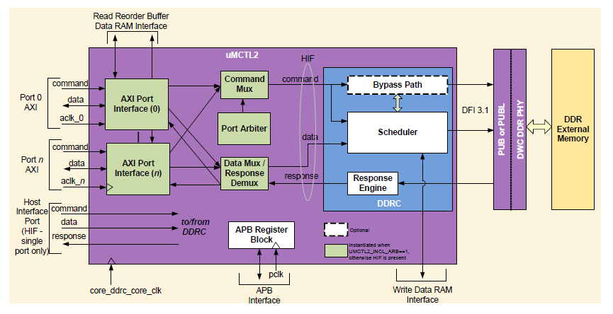
Figure 15-1 DRAM Controller Functional Blocks
The uMCTL2 contains the following main architectural components
...
- DPCU_DFI_CMD_DEC: This module is used to decode DFI commands from DRAM controller for DRAM device.
- DPCU_APHY_INIT: DPCU_APHY_INIT controls the initial flow for analog part (APHY).
- DPCU_DATA_TRAINING: This is the crucial part of DDRPHY, and it is used to do data training, which is the process to acquire optimal timing between signals for DRAM write/read transactions.
- DPCU_CMD_ISSUE: This module works like a lite DRAM controller. It can generate DRAM commands and the timing between those commands is guaranteed to meet DRAM specification.
- DPCU_VT_DETECT: Since process, voltage and temperature can deviate the delay of delay cells, this module is used to compensate those non-ideal effects.
- DPCU_SW_UPDATE: If the system need to change some settings of delay cells by software, this module can update those settings in a suitable period.
- DPCU_RGST_BUS: The communication interface between CPU and DDRPHY.
- DPCU_APHY_WRAPPER: The interface between DPCU and APHY.
- DDR_APHY: Analog part of DDRPHY which provide the interface with DDR device.
...
- .
...
31:27
...
RW
...
control DRAM A3 swap
...
select one DRAM BUS signal to through DRAM A3 pin;
...
default value is 0xc, represent DRAM A3 signal through
...
DRAM A3 pin;
...
0x0: select DRAM CKE signal through DRAM A3 pin;
...
0x1: select DRAM ODT signal through DRAM A3 pin;
...
0x2: select DRAM CS N signal through DRAM A3 pin;
...
0x3: select DRAM RAS N signal through DRAM A3 pin;
...
0x4: select DRAM CAS N signal through DRAM A3 pin;
...
0x5: select DRAM WE N signal through DRAM A3 pin;
...
0x6: select DRAM BA0 signal through DRAM A3 pin;
...
0x7: select DRAM BA1 signal through DRAM A3 pin;
...
0x8: select DRAM BA2 signal through DRAM A3 pin;
...
0x9: select DRAM A0 signal through DRAM A3 pin;
...
0xa: select DRAM A1 signal through DRAM A3 pin;
...
0xb: select DRAM A2 signal through DRAM A3 pin;
...
0xc: select DRAM A3 signal through DRAM A3 pin;
...
0xd: select DRAM A4 signal through DRAM A3 pin;
...
0xe: select DRAM A5 signal through DRAM A3 pin;
...
0xf: select DRAM A6 signal through DRAM A3 pin;
...
0x10: select DRAM A7 signal through DRAM A3 pin;
...
0x11: select DRAM A8 signal through DRAM A3 pin;
...
0x12: select DRAM A9 signal through DRAM A3 pin;
...
0x13: select DRAM A10 signal through DRAM A3 pin;
...
0x14: select DRAM A11 signal through DRAM A3 pin;
...
0x15: select DRAM A12 signal through DRAM A3 pin;
...
0x16: select DRAM A13 signal through DRAM A3 pin;
...
0x17: select DRAM A14 signal through DRAM A3 pin;
...
0x18: select DRAM A15 signal through DRAM A3 pin;
15.4 Registers Map
15.4.1 Registers Memory Map
...
Address
...
Group No.
...
Register Name
...
Description
...
0x9C001900
...
G50.0
...
dpcu glo set
...
DPCU Global Setting
...
0x9C001904
...
G50.1
...
dpcu init ctrl
...
DPCU Initial control
...
0x9C001908
...
G50.2
...
dpcu init status
...
DPCU Initial status
...
0x9C00190C
...
G50.3
...
dpcu aphy cnter
...
DPCU APHY Counter
...
0x9C001910
...
G50.4
...
dpcu ddl calib set
...
DPCU DDL Calibration Global Setting
...
0x9C001914
...
G50.5
...
dpcu sscpll ctrl1
...
DPCU SSCPLL setting - 1
...
0x9C001918
...
G50.6
...
dpcu sscpll ctrl2
...
DPCU SSCPLL setting - 2
...
0x9C00191C
...
G50.7
...
reserved
...
DPCU Global reserved
...
0x9C001920
...
G50.8
...
dpcu aphy glo
...
APHY - Global
...
0x9C001924
...
G50.9
...
dpcu aphy macro0
...
APHY - MACRO Status Output - 0
...
0x9C001928
...
G50.10
...
dpcu aphy macro1
...
APHY - MACRO Status Output - 1
...
0x9C00192C
...
G50.11
...
dpcu aphy mpll0
...
APHY - MPLL 0
...
0x9C001930
...
G50.12
...
dpcu aphy mpll1
...
APHY - MPLL 1
...
0x9C001934
...
G50.13
...
dpcu aphy ctcal0
...
APHY - CTCAL 0
...
0x9C001938
...
G50.14
...
dpcu aphy ctcal1
...
APHY - CTCAL 1
...
0x9C00193C
...
G50.15
...
reserved
...
reserved
...
0x9C001940
...
G50.16
...
dpcu aphy div
...
APHY - DIVIDER
...
0x9C001944
...
G50.17
...
dpcu aphy ddl value
...
APHY - DDL Static DLY Value
...
0x9C001948
...
G50.18
...
dpcu aphy iopad0
...
APHY - IOPAD 0 PZQ
...
0x9C00194C
...
G50.19
...
dpcu aphy iopad1
...
APHY - IOPAD 1 PZQ VREF
...
0x9C001950
...
G50.20
...
dpcu aphy iopad2
...
APHY - IOPAD 2 ADDR and CMD
...
0x9C001954
...
G50.21
...
dpcu aphy iopad3
...
APHY - IOPAD 3 DX
...
0x9C001958
...
G50.22
...
dpcu aphy iopad4
...
APHY - IOPAD 4 reserved
...
0x9C00195C
...
G50.23
...
dpcu aphy debug mode
...
APHY - DEBUG mode
...
0x9C001960
...
G50.24
...
dpcu aphy osc mode
...
APHY - OSC mode
...
0x9C001964
...
G50.25
...
dpcu aphy dummy port
...
APHY - DUMMY ports
...
0x9C001968
...
G50.26
...
reserved
...
reserved
...
0x9C00196C
...
G50.27
...
reserved
...
reserved
...
0x9C001970
...
G50.28
...
reserved
...
reserved
...
0x9C001974
...
G50.29
...
reserved
...
reserved
...
0x9C001978
...
G50.30
...
reserved
...
reserved
...
0x9C00197C
...
G50.31
...
reserved
...
reserved
15.4.2 Registers Description
...
RF MODE EN
...
18
...
RW
...
DFI Interface signal transfer mode
0: controller and PHY use posedge of DFI clock
1: controller use negedge of DFI clock; PHY use posedge of DFI clock
...
RGST AI PZQ IO DIS
...
17
...
RW
...
disable IO during PZQ calibration
...
DIS VT CALIB
...
4
...
RW
...
Disable VT dynamic calibration function
0 : enable (default)
1 : disable,
...
RESERVED
...
3
...
RO
...
reserved
...
RESERVED
...
1
...
RW
...
reserved
...
APHY INIT ERROR INFO
...
19:16
...
RO
...
APHY initial error information
0 : no error (default)
1 : trigger CI error
2 : initial error others : reserved
...
APHY INIT STATE
...
15:12
...
RO
...
Debug information. Current DPCU AI main FSM value
...
Field Name
...
Access
...
Description
...
DPCU RST TIMMER
...
RW
...
no specific function at V2.0.
...
Field Name
...
Bit
...
Access
...
Description
...
DPCU RI SSCPLL GAIN
...
27:19
...
RW
...
Field Name
...
Access
...
Description
...
APHY RO CTCAL DDR R
...
RO
...
code value of ddr programmable delay line
...
APHY RO PZQ ZCTRL
...
23:8
...
RO
...
Status of calibration result (coarse adjust):
APHY RO PZQ ZCTRL[3:0] select the pull-down output impedance
APHY RO PZQ ZCTRL[7:4] select the pull-up output impedance
APHY RO PZQ ZCTRL[11:8] select the pull-down ODT impedance
APHY RO PZQ ZCTRL[15:12] select the pull-up ODT Impedance
...
APHY RO PZQ ZLSB
...
7:4
...
RO
...
Status of calibration result (fine adjust):
...
DPCU RI ACK BDD DLY
...
21:16
...
RW
...
address and command bit deskew delay
...
DPCU RI VREF MUX
...
29
...
RW
...
Select external VREF or internal VREF.
0 : select internal VREF, enable analog test function (de- fault)
1 : select external VREF, disable analog test function
...
DPCU RI PZQ OVRD DATA
...
28:9
...
RW
...
Impedance Over-Ride Data: Data used to directly drive the impedance control.
DPCU RI PZQ OVRD DATA[4:0] : select the pull-down output impedance
DPCU RI PZQ OVRD DATA[9:5] : select the pull-up out- put impedance
DPCU RI PZQ OVRD DATA[14:10] :select the pull- down ODT impedance
DPCU RI PZQ OVRD DATA[19:15] : select the pull-up
ODT impedance
(low bit is fine control)
...
DPCU RI PZQ OVRD EN
...
8
...
RW
...
Impedance Direct calibration Enable
0 : Direct calibration (default)
1 : allows users to directly drive the impedance control using the data programmed in the ZQDATA field (setting zctrl ovrd data[19:0])
...
DPCU RI PZQ ZPROG
...
7:0
...
RW
...
DDRIO impedance setting
...
DPCU RI CKE PD RCV
...
20
...
RW
...
Power down DDRIO reciver of clock enable PAD
...
50.23 APHY - DEBUG mode (dpcu aphy debug mode)
Address: 0x9C00195C
...
Address: 0x9C001960
Reset: 0x0000 000C
...
Field Name
...
Bit
...
Access
...
Description
...
RO
...
29:25
...
RW
...
control DRAM BA0 swap
...
select one DRAM BUS signal to through DRAM BA0 pin;
...
default value is 0x6, represent DRAM BA0 signal through
...
DRAM BA0 pin;
...
0x0: select DRAM CKE signal through DRAM BA0 pin;
...
0x1: select DRAM ODT signal through DRAM BA0 pin;
...
0x2: select DRAM CS N signal through DRAM BA0 pin;
...
0x3: select DRAM RAS N signal through DRAM BA0 pin;
...
0x4: select DRAM CAS N signal through DRAM BA0 pin;
...
0x5: select DRAM WE N signal through DRAM BA0 pin;
...
0x6: select DRAM BA0 signal through DRAM BA0 pin;
...
0x7: select DRAM BA1 signal through DRAM BA0 pin;
...
0x8: select DRAM BA2 signal through DRAM BA0 pin;
...
0x9: select DRAM A0 signal through DRAM BA0 pin;
...
0xa: select DRAM A1 signal through DRAM BA0 pin;
...
0xb: select DRAM A2 signal through DRAM BA0 pin;
...
0xc: select DRAM A3 signal through DRAM BA0 pin;
...
0xd: select DRAM A4 signal through DRAM BA0 pin;
...
0xe: select DRAM A5 signal through DRAM BA0 pin;
...
0xf: select DRAM A6 signal through DRAM BA0 pin;
...
0x10: select DRAM A7 signal through DRAM BA0 pin;
...
0x11: select DRAM A8 signal through DRAM BA0 pin;
...
0x12: select DRAM A9 signal through DRAM BA0 pin;
...
0x13: select DRAM A10 signal through DRAM BA0 pin;
...
0x14: select DRAM A11 signal through DRAM BA0 pin;
...
0x15: select DRAM A12 signal through DRAM BA0 pin;
...
0x16: select DRAM A13 signal through DRAM BA0 pin;
...
0x17: select DRAM A14 signal through DRAM BA0 pin;
...
0x18: select DRAM A15 signal through DRAM BA0 pin;
...
control DRAM WE N swap
select one DRAM BUS signal to through DRAM WE N pin;
default value is 0x5, represent DRAM WE N signal through DRAM WE N pin;
0x0: select DRAM CKE signal through DRAM WE N pin;
0x1: select DRAM ODT signal through DRAM WE N pin;
0x2: select DRAM CS N signal through DRAM WE N pin;
0x3: select DRAM RAS N signal through DRAM WE N pin;
0x4: select DRAM CAS N signal through DRAM WE N pin;
0x5: select DRAM WE N signal through DRAM WE N pin;
0x6: select DRAM BA0 signal through DRAM WE N pin;
0x7: select DRAM BA1 signal through DRAM WE N pin;
0x8: select DRAM BA2 signal through DRAM WE N pin;
0x9: select DRAM A0 signal through DRAM WE N pin;
0xa: select DRAM A1 signal through DRAM WE N pin;
0xb: select DRAM A2 signal through DRAM WE N pin;
0xc: select DRAM A3 signal through DRAM WE N pin;
0xd: select DRAM A4 signal through DRAM WE N pin;
0xe: select DRAM A5 signal through DRAM WE N pin;
0xf: select DRAM A6 signal through DRAM WE N pin;
0x10: select DRAM A7 signal through DRAM WE N pin;
0x11: select DRAM A8 signal through DRAM WE N pin;
0x12: select DRAM A9 signal through DRAM WE N pin;
0x13: select DRAM A10 signal through DRAM WE N pin;
0x14: select DRAM A11 signal through DRAM WE N pin;
0x15: select DRAM A12 signal through DRAM WE N pin;
0x16: select DRAM A13 signal through DRAM WE N pin;
0x17: select DRAM A14 signal through DRAM WE N pin;
0x18: select DRAM A15 signal through DRAM WE N pin;
...
control DRAM CAS N swap
select one DRAM BUS signal to through DRAM CAS N pin;
default value is 0x4, represent DRAM CAS N signal through DRAM CAS N pin;
0x0: select DRAM CKE signal through DRAM CAS N pin;
0x1: select DRAM ODT signal through DRAM CAS N pin;
0x2: select DRAM CS N signal through DRAM CAS N pin;
0x3: select DRAM RAS N signal through DRAM CAS N pin;
0x4: select DRAM CAS N signal through DRAM CAS Npin;
0x5: select DRAM WE N signal through DRAM CAS N pin;
0x6: select DRAM BA0 signal through DRAM CAS N pin;
0x7: select DRAM BA1 signal through DRAM CAS N pin;
0x8: select DRAM BA2 signal through DRAM CAS N pin;
0x9: select DRAM A0 signal through DRAM CAS N pin;
0xa: select DRAM A1 signal through DRAM CAS N pin;
0xb: select DRAM A2 signal through DRAM CAS N pin;
0xc: select DRAM A3 signal through DRAM CAS N pin;
0xd: select DRAM A4 signal through DRAM CAS N pin;
0xe: select DRAM A5 signal through DRAM CAS N pin;
0xf: select DRAM A6 signal through DRAM CAS N pin;
0x10: select DRAM A7 signal through DRAM CAS N pin;
0x11: select DRAM A8 signal through DRAM CAS N pin;
0x12: select DRAM A9 signal through DRAM CAS N pin;
0x13: select DRAM A10 signal through DRAM CAS N pin;
0x14: select DRAM A11 signal through DRAM CAS N pin;
0x15: select DRAM A12 signal through DRAM CAS N pin;
0x16: select DRAM A13 signal through DRAM CAS N pin;
0x17: select DRAM A14 signal through DRAM CAS N pin;
0x18: select DRAM A15 signal through DRAM CAS N pin;
...
control DRAM RAS N swap
select one DRAM BUS signal to through DRAM RAS N pin;
default value is 0x3, represent DRAM RAS N signal through DRAM RAS N pin;
0x0: select DRAM CKE signal through DRAM RAS N pin;
0x1: select DRAM ODT signal through DRAM RAS N pin;
0x2: select DRAM CS N signal through DRAM RAS N pin;
0x3: select DRAM RAS N signal through DRAM RAS N pin;
0x4: select DRAM CAS N signal through DRAM RAS N pin;
0x5: select DRAM WE N signal through DRAM RAS N pin;
0x6: select DRAM BA0 signal through DRAM RAS N pin;
0x7: select DRAM BA1 signal through DRAM RAS N pin;
0x8: select DRAM BA2 signal through DRAM RAS N pin;
0x9: select DRAM A0 signal through DRAM RAS N pin;
0xa: select DRAM A1 signal through DRAM RAS N pin;
0xb: select DRAM A2 signal through DRAM RAS N pin;
0xc: select DRAM A3 signal through DRAM RAS N pin;
0xd: select DRAM A4 signal through DRAM RAS N pin;
0xe: select DRAM A5 signal through DRAM RAS N pin;
0xf: select DRAM A6 signal through DRAM RAS N pin;
0x10: select DRAM A7 signal through DRAM RAS N pin;
0x11: select DRAM A8 signal through DRAM RAS N pin;
0x12: select DRAM A9 signal through DRAM RAS N pin;
0x13: select DRAM A10 signal through DRAM RAS N pin;
0x14: select DRAM A11 signal through DRAM RAS N pin;
0x15: select DRAM A12 signal through DRAM RAS N pin;
0x16: select DRAM A13 signal through DRAM RAS N pin;
0x17: select DRAM A14 signal through DRAM RAS N pin;
0x18: select DRAM A15 signal through DRAM RAS N pin;
...
control DRAM CS N swap
select one DRAM BUS signal to through DRAM CS N pin;
default value is 0x2, represent DRAM CS N signal through DRAM CS N pin;
0x0: select DRAM CKE signal through DRAM CS N pin;
0x1: select DRAM ODT signal through DRAM CS N pin;
0x2: select DRAM CS N signal through DRAM CS N pin;
0x3:select DRAM RAS N signal through DRAM CS N pin
0x4:select DRAM CAS N signal through DRAM CS N pin
0x5:select DRAM WE N signal through DRAM CS N pin
0x6: select DRAM BA0 signal through DRAM CS N pin;
0x7: select DRAM BA1 signal through DRAM CS N pin;
0x8: select DRAM BA2 signal through DRAM CS N pin;
0x9: select DRAM A0 signal through DRAM CS N pin;
0xa: select DRAM A1 signal through DRAM CS N pin;
0xb: select DRAM A2 signal through DRAM CS N pin;
0xc: select DRAM A3 signal through DRAM CS N pin;
0xd: select DRAM A4 signal through DRAM CS N pin;
0xe: select DRAM A5 signal through DRAM CS N pin;
0xf: select DRAM A6 signal through DRAM CS N pin;
0x10: select DRAM A7 signal through DRAM CS N pin;
0x11: select DRAM A8 signal through DRAM CS N pin;
0x12: select DRAM A9 signal through DRAM CS N pin;
0x13: select DRAM A10 signal through DRAM CS N pin;
0x14: select DRAM A11 signal through DRAM CS N pin;
0x15: select DRAM A12 signal through DRAM CS N pin;
0x16: select DRAM A13 signal through DRAM CS N pin;
0x17: select DRAM A14 signal through DRAM CS N pin;
0x18: select DRAM A15 signal through DRAM CS N pin;
...
control DRAM ODT swap
select one DRAM BUS signal to through DRAM ODT pin;
default value is 0x1, represent DRAM ODT signal through DRAM ODT pin;
0x0: select DRAM CKE signal through DRAM ODT pin;
0x1: select DRAM ODT signal through DRAM ODT pin;
0x2: select DRAM CS N signal through DRAM ODT pin;
0x3:select DRAM RAS N signal through DRAM ODT pin
0x4:select DRAM CAS N signal through DRAM ODT pin
0x5: select DRAM WE N signal through DRAM ODT pin;
0x6: select DRAM BA0 signal through DRAM ODT pin;
0x7: select DRAM BA1 signal through DRAM ODT pin;
0x8: select DRAM BA2 signal through DRAM ODT pin;
0x9: select DRAM A0 signal through DRAM ODT pin;
0xa: select DRAM A1 signal through DRAM ODT pin;
0xb: select DRAM A2 signal through DRAM ODT pin;
0xc: select DRAM A3 signal through DRAM ODT pin;
0xd: select DRAM A4 signal through DRAM ODT pin;
0xe: select DRAM A5 signal through DRAM ODT pin;
0xf: select DRAM A6 signal through DRAM ODT pin;
0x10: select DRAM A7 signal through DRAM ODT pin;
0x11: select DRAM A8 signal through DRAM ODT pin;
0x12: select DRAM A9 signal through DRAM ODT pin;
0x13: select DRAM A10 signal through DRAM ODT pin;
0x14: select DRAM A11 signal through DRAM ODT pin;
0x15: select DRAM A12 signal through DRAM ODT pin;
0x16: select DRAM A13 signal through DRAM ODT pin;
0x17: select DRAM A14 signal through DRAM ODT pin;
0x18: select DRAM A15 signal through DRAM ODT pin;
...
31:27
...
RW
...
control DRAM A3 swap
...
select one DRAM BUS signal to through DRAM A3 pin;
...
default value is 0xc, represent DRAM A3 signal through
...
DRAM A3 pin;
...
0x0: select DRAM CKE signal through DRAM A3 pin;
...
0x1: select DRAM ODT signal through DRAM A3 pin;
...
0x2: select DRAM CS N signal through DRAM A3 pin;
...
0x3: select DRAM RAS N signal through DRAM A3 pin;
...
0x4: select DRAM CAS N signal through DRAM A3 pin;
...
0x5: select DRAM WE N signal through DRAM A3 pin;
...
0x6: select DRAM BA0 signal through DRAM A3 pin;
...
0x7: select DRAM BA1 signal through DRAM A3 pin;
...
0x8: select DRAM BA2 signal through DRAM A3 pin;
...
0x9: select DRAM A0 signal through DRAM A3 pin;
...
0xa: select DRAM A1 signal through DRAM A3 pin;
...
0xb: select DRAM A2 signal through DRAM A3 pin;
...
0xc: select DRAM A3 signal through DRAM A3 pin;
...
0xd: select DRAM A4 signal through DRAM A3 pin;
...
0xe: select DRAM A5 signal through DRAM A3 pin;
...
0xf: select DRAM A6 signal through DRAM A3 pin;
...
0x10: select DRAM A7 signal through DRAM A3 pin;
...
0x11: select DRAM A8 signal through DRAM A3 pin;
...
0x12: select DRAM A9 signal through DRAM A3 pin;
...
0x13: select DRAM A10 signal through DRAM A3 pin;
...
0x14: select DRAM A11 signal through DRAM A3 pin;
...
0x15: select DRAM A12 signal through DRAM A3 pin;
...
0x16: select DRAM A13 signal through DRAM A3 pin;
...
0x17: select DRAM A14 signal through DRAM A3 pin;
...
0x18: select DRAM A15 signal through DRAM A3 pin;
...
26:22
...
RW
...
control DRAM A2 swap
...
select one DRAM BUS signal to through DRAM A2 pin;
...
default value is 0xb, represent DRAM A2 signal through
...
DRAM A2 pin;
...
0x0: select DRAM CKE signal through DRAM A2 pin;
...
0x1: select DRAM ODT signal through DRAM A2 pin;
...
0x2: select DRAM CS N signal through DRAM A2 pin;
...
0x3: select DRAM RAS N signal through DRAM A2 pin;
...
0x4: select DRAM CAS N signal through DRAM A2 pin;
...
0x5: select DRAM WE N signal through DRAM A2 pin;
...
0x6: select DRAM BA0 signal through DRAM A2 pin;
...
0x7: select DRAM BA1 signal through DRAM A2 pin;
...
0x8: select DRAM BA2 signal through DRAM A2 pin;
...
0x9: select DRAM A0 signal through DRAM A2 pin;
...
0xa: select DRAM A1 signal through DRAM A2 pin;
...
0xb: select DRAM A2 signal through DRAM A2 pin;
...
0xc: select DRAM A3 signal through DRAM A2 pin;
...
0xd: select DRAM A4 signal through DRAM A2 pin;
...
0xe: select DRAM A5 signal through DRAM A2 pin;
...
0xf: select DRAM A6 signal through DRAM A2 pin;
...
0x10: select DRAM A7 signal through DRAM A2 pin;
...
0x11: select DRAM A8 signal through DRAM A2 pin;
...
0x12: select DRAM A9 signal through DRAM A2 pin;
...
0x13: select DRAM A10 signal through DRAM A2 pin;
...
0x14: select DRAM A11 signal through DRAM A2 pin;
...
0x15: select DRAM A12 signal through DRAM A2 pin;
...
0x16: select DRAM A13 signal through DRAM A2 pin;
...
0x17: select DRAM A14 signal through DRAM A2 pin;
...
0x18: select DRAM A15 signal through DRAM A2 pin;
...
21:17
...
RW
...
control DRAM A1 swap
...
select one DRAM BUS signal to through DRAM A1 pin;
...
default value is 0xa, represent DRAM A1 signal through
...
DRAM A1 pin;
...
0x0: select DRAM CKE signal through DRAM A1 pin;
...
0x1: select DRAM ODT signal through DRAM A1 pin;
...
0x2: select DRAM CS N signal through DRAM A1 pin;
...
0x3: select DRAM RAS N signal through DRAM A1 pin;
...
0x4: select DRAM CAS N signal through DRAM A1 pin;
...
0x5: select DRAM WE N signal through DRAM A1 pin;
...
0x6: select DRAM BA0 signal through DRAM A1 pin;
...
0x7: select DRAM BA1 signal through DRAM A1 pin;
...
0x8: select DRAM BA2 signal through DRAM A1 pin;
...
0x9: select DRAM A0 signal through DRAM A1 pin;
...
0xa: select DRAM A1 signal through DRAM A1 pin;
...
0xb: select DRAM A2 signal through DRAM A1 pin;
...
0xc: select DRAM A3 signal through DRAM A1 pin;
...
0xd: select DRAM A4 signal through DRAM A1 pin;
...
0xe: select DRAM A5 signal through DRAM A1 pin;
...
0xf: select DRAM A6 signal through DRAM A1 pin;
...
0x10: select DRAM A7 signal through DRAM A1 pin;
...
0x11: select DRAM A8 signal through DRAM A1 pin;
...
0x12: select DRAM A9 signal through DRAM A1 pin;
...
0x13: select DRAM A10 signal through DRAM A1 pin;
...
0x14: select DRAM A11 signal through DRAM A1 pin;
...
0x15: select DRAM A12 signal through DRAM A1 pin;
...
0x16: select DRAM A13 signal through DRAM A1 pin;
...
0x17: select DRAM A14 signal through DRAM A1 pin;
...
0x18: select DRAM A15 signal through DRAM A1 pin;
...
16:12
...
RW
...
control DRAM A0 swap
...
select one DRAM BUS signal to through DRAM A0 pin;
...
default value is 0x9, represent DRAM A0 signal through
...
DRAM A0 pin;
...
0x0: select DRAM CKE signal through DRAM A0 pin;
...
0x1: select DRAM ODT signal through DRAM A0 pin;
...
0x2: select DRAM CS N signal through DRAM A0 pin;
...
0x3: select DRAM RAS N signal through DRAM A0 pin;
...
0x4: select DRAM CAS N signal through DRAM A0 pin;
...
0x5: select DRAM WE N signal through DRAM A0 pin;
...
0x6: select DRAM BA0 signal through DRAM A0 pin;
...
0x7: select DRAM BA1 signal through DRAM A0 pin;
...
0x8: select DRAM BA2 signal through DRAM A0 pin;
...
0x9: select DRAM A0 signal through DRAM A0 pin;
...
0xa: select DRAM A1 signal through DRAM A0 pin;
...
0xb: select DRAM A2 signal through DRAM A0 pin;
...
0xc: select DRAM A3 signal through DRAM A0 pin;
...
0xd: select DRAM A4 signal through DRAM A0 pin;
...
0xe: select DRAM A5 signal through DRAM A0 pin;
...
0xf: select DRAM A6 signal through DRAM A0 pin;
...
0x10: select DRAM A7 signal through DRAM A0 pin;
...
0x11: select DRAM A8 signal through DRAM A0 pin;
...
0x12: select DRAM A9 signal through DRAM A0 pin;
...
0x13: select DRAM A10 signal through DRAM A0 pin;
...
0x14: select DRAM A11 signal through DRAM A0 pin;
...
0x15: select DRAM A12 signal through DRAM A0 pin;
...
0x16: select DRAM A13 signal through DRAM A0 pin;
...
0x17: select DRAM A14 signal through DRAM A0 pin;
...
0x18: select DRAM A15 signal through DRAM A0 pin;
...
11:7
...
RW
...
control DRAM BA2 swap
...
select one DRAM BUS signal to through DRAM BA2 pin;
...
default value is 0x8, represent DRAM BA2 signal through
...
DRAM BA2 pin;
...
0x0: select DRAM CKE signal through DRAM BA2 pin;
...
0x1: select DRAM ODT signal through DRAM BA2 pin;
...
0x2: select DRAM CS N signal through DRAM BA2 pin;
...
0x3: select DRAM RAS N signal through DRAM BA2 pin;
...
0x4: select DRAM CAS N signal through DRAM BA2 pin;
...
0x5: select DRAM WE N signal through DRAM BA2 pin;
...
0x6: select DRAM BA0 signal through DRAM BA2 pin;
...
0x7: select DRAM BA1 signal through DRAM BA2 pin;
...
0x8: select DRAM BA2 signal through DRAM BA2 pin;
...
0x9: select DRAM A0 signal through DRAM BA2 pin;
...
0xa: select DRAM A1 signal through DRAM BA2 pin;
...
0xb: select DRAM A2 signal through DRAM BA2 pin;
...
0xc: select DRAM A3 signal through DRAM BA2 pin;
...
0xd: select DRAM A4 signal through DRAM BA2 pin;
...
0xe: select DRAM A5 signal through DRAM BA2 pin;
...
0xf: select DRAM A6 signal through DRAM BA2 pin;
...
0x10: select DRAM A7 signal through DRAM BA2 pin;
...
0x11: select DRAM A8 signal through DRAM BA2 pin;
...
0x12: select DRAM A9 signal through DRAM BA2 pin;
...
0x13: select DRAM A10 signal through DRAM BA2 pin;
...
0x14: select DRAM A11 signal through DRAM BA2 pin;
...
0x15: select DRAM A12 signal through DRAM BA2 pin;
...
0x16: select DRAM A13 signal through DRAM BA2 pin;
...
0x17: select DRAM A14 signal through DRAM BA2 pin;
...
0x18: select DRAM A15 signal through DRAM BA2 pin;
...
BA1 SWAP
...
6:2
...
RW
...
control DRAM BA1 swap
select one DRAM BUS signal to through DRAM BA1 pin;
default value is 0x7, represent DRAM BA1 signal through DRAM BA1 pin;
0x0: select DRAM CKE signal through DRAM BA1 pin;
0x1: select DRAM ODT signal through DRAM BA1 pin;
0x2: select DRAM CS N signal through DRAM BA1 pin;
0x3: select DRAM RAS N signal through DRAM BA1 pin;
0x4: select DRAM CAS N signal through DRAM BA1 pin;
0x5: select DRAM WE N signal through DRAM BA1 pin;
0x6: select DRAM BA0 signal through DRAM BA1 pin;
0x7: select DRAM BA1 signal through DRAM BA1 pin;
0x8: select DRAM BA2 signal through DRAM BA1 pin;
0x9: select DRAM A0 signal through DRAM BA1 pin;
0xa: select DRAM A1 signal through DRAM BA1 pin;
0xb: select DRAM A2 signal through DRAM BA1 pin;
0xc: select DRAM A3 signal through DRAM BA1 pin;
0xd: select DRAM A4 signal through DRAM BA1 pin;
0xe: select DRAM A5 signal through DRAM BA1 pin;
0xf: select DRAM A6 signal through DRAM BA1 pin;
0x10: select DRAM A7 signal through DRAM BA1 pin;
0x11: select DRAM A8 signal through DRAM BA1 pin;
0x12: select DRAM A9 signal through DRAM BA1 pin;
0x13: select DRAM A10 signal through DRAM BA1 pin;
0x14: select DRAM A11 signal through DRAM BA1 pin;
0x15: select DRAM A12 signal through DRAM BA1 pin;
0x16: select DRAM A13 signal through DRAM BA1 pin;
0x17: select DRAM A14 signal through DRAM BA1 pin;
0x18: select DRAM A15 signal through DRAM BA1 pin;
...
RESERVED
...
1
...
RO
...
reserved
...
A9 SWAP
...
29:25
...
RW
...
control DRAM A9 swap
...
select one DRAM BUS signal to through DRAM A9 pin;
...
default value is 0x12, represent DRAM A9 signal through
...
DRAM A9 pin;
...
0x0: select DRAM CKE signal through DRAM A9 pin;
...
0x1: select DRAM ODT signal through DRAM A9 pin;
...
0x2: select DRAM CS N signal through DRAM A9 pin;
...
0x3: select DRAM RAS N signal through DRAM A9 pin;
...
0x4: select DRAM CAS N signal through DRAM A9 pin;
...
0x5: select DRAM WE N signal through DRAM A9 pin;
...
0x6: select DRAM BA0 signal through DRAM A9 pin;
...
0x7: select DRAM BA1 signal through DRAM A9 pin;
...
0x8: select DRAM BA2 signal through DRAM A9 pin;
...
0x9: select DRAM A0 signal through DRAM A9 pin;
...
0xa: select DRAM A1 signal through DRAM A9 pin;
...
0xb: select DRAM A2 signal through DRAM A9 pin;
...
0xc: select DRAM A3 signal through DRAM A9 pin;
...
0xd: select DRAM A4 signal through DRAM A9 pin;
...
0xe: select DRAM A5 signal through DRAM A9 pin;
...
0xf: select DRAM A6 signal through DRAM A9 pin;
...
0x10: select DRAM A7 signal through DRAM A9 pin;
...
0x11: select DRAM A8 signal through DRAM A9 pin;
...
0x12: select DRAM A9 signal through DRAM A9 pin;
...
0x13: select DRAM A10 signal through DRAM A9 pin;
...
0x14: select DRAM A11 signal through DRAM A9 pin;
...
0x15: select DRAM A12 signal through DRAM A9 pin;
...
0x16: select DRAM A13 signal through DRAM A9 pin;
...
0x17: select DRAM A14 signal through DRAM A9 pin;
...
0x18: select DRAM A15 signal through DRAM A9 pin;
...
24:20
...
RW
...
control DRAM A8 swap
...
select one DRAM BUS signal to through DRAM A8 pin;
...
default value is 0x11, represent DRAM A8 signal through
...
DRAM A8 pin;
...
0x0: select DRAM CKE signal through DRAM A8 pin;
...
0x1: select DRAM ODT signal through DRAM A8 pin;
...
0x2: select DRAM CS N signal through DRAM A8 pin;
...
0x3: select DRAM RAS N signal through DRAM A8 pin;
...
0x4: select DRAM CAS N signal through DRAM A8 pin;
...
0x5: select DRAM WE N signal through DRAM A8 pin;
...
0x6: select DRAM BA0 signal through DRAM A8 pin;
...
0x7: select DRAM BA1 signal through DRAM A8 pin;
...
0x8: select DRAM BA2 signal through DRAM A8 pin;
...
0x9: select DRAM A0 signal through DRAM A8 pin;
...
0xa: select DRAM A1 signal through DRAM A8 pin;
...
0xb: select DRAM A2 signal through DRAM A8 pin;
...
0xc: select DRAM A3 signal through DRAM A8 pin;
...
0xd: select DRAM A4 signal through DRAM A8 pin;
...
0xe: select DRAM A5 signal through DRAM A8 pin;
...
0xf: select DRAM A6 signal through DRAM A8 pin;
...
0x10: select DRAM A7 signal through DRAM A8 pin;
...
0x11: select DRAM A8 signal through DRAM A8 pin;
...
0x12: select DRAM A9 signal through DRAM A8 pin;
...
0x13: select DRAM A10 signal through DRAM A8 pin;
...
0x14: select DRAM A11 signal through DRAM A8 pin;
...
0x15: select DRAM A12 signal through DRAM A8 pin;
...
0x16: select DRAM A13 signal through DRAM A8 pin;
...
0x17: select DRAM A14 signal through DRAM A8 pin;
...
0x18: select DRAM A15 signal through DRAM A8 pin;
...
19:15
...
RW
...
control DRAM A7 swap
...
select one DRAM BUS signal to through DRAM A7 pin;
...
default value is 0x10, represent DRAM A7 signal through
...
DRAM A7 pin;
...
0x0: select DRAM CKE signal through DRAM A7 pin;
...
0x1: select DRAM ODT signal through DRAM A7 pin;
...
0x2: select DRAM CS N signal through DRAM A7 pin;
...
0x3: select DRAM RAS N signal through DRAM A7 pin;
...
0x4: select DRAM CAS N signal through DRAM A7 pin;
...
0x5: select DRAM WE N signal through DRAM A7 pin;
...
0x6: select DRAM BA0 signal through DRAM A7 pin;
...
0x7: select DRAM BA1 signal through DRAM A7 pin;
...
0x8: select DRAM BA2 signal through DRAM A7 pin;
...
0x9: select DRAM A0 signal through DRAM A7 pin;
...
0xa: select DRAM A1 signal through DRAM A7 pin;
...
0xb: select DRAM A2 signal through DRAM A7 pin;
...
0xc: select DRAM A3 signal through DRAM A7 pin;
...
0xd: select DRAM A4 signal through DRAM A7 pin;
...
0xe: select DRAM A5 signal through DRAM A7 pin;
...
0xf: select DRAM A6 signal through DRAM A7 pin;
...
0x10: select DRAM A7 signal through DRAM A7 pin;
...
0x11: select DRAM A8 signal through DRAM A7 pin;
...
0x12: select DRAM A9 signal through DRAM A7 pin;
...
0x13: select DRAM A10 signal through DRAM A7 pin;
...
0x14: select DRAM A11 signal through DRAM A7 pin;
...
0x15: select DRAM A12 signal through DRAM A7 pin;
...
0x16: select DRAM A13 signal through DRAM A7 pin;
...
0x17: select DRAM A14 signal through DRAM A7 pin;
...
0x18: select DRAM A15 signal through DRAM A7 pin;
...
14:10
...
RW
...
control DRAM A6 swap
...
select one DRAM BUS signal to through DRAM A6 pin;
...
default value is 0xf, represent DRAM A6 signal through
...
DRAM A6 pin;
...
0x0: select DRAM CKE signal through DRAM A6 pin;
...
0x1: select DRAM ODT signal through DRAM A6 pin;
...
0x2: select DRAM CS N signal through DRAM A6 pin;
...
0x3: select DRAM RAS N signal through DRAM A6 pin;
...
0x4: select DRAM CAS N signal through DRAM A6 pin;
...
0x5: select DRAM WE N signal through DRAM A6 pin;
...
0x6: select DRAM BA0 signal through DRAM A6 pin;
...
0x7: select DRAM BA1 signal through DRAM A6 pin;
...
0x8: select DRAM BA2 signal through DRAM A6 pin;
...
0x9: select DRAM A0 signal through DRAM A6 pin;
...
0xa: select DRAM A1 signal through DRAM A6 pin;
...
0xb: select DRAM A2 signal through DRAM A6 pin;
...
0xc: select DRAM A3 signal through DRAM A6 pin;
...
0xd: select DRAM A4 signal through DRAM A6 pin;
...
0xe: select DRAM A5 signal through DRAM A6 pin;
...
0xf: select DRAM A6 signal through DRAM A6 pin;
...
0x10: select DRAM A7 signal through DRAM A6 pin;
...
0x11: select DRAM A8 signal through DRAM A6 pin;
...
0x12: select DRAM A9 signal through DRAM A6 pin;
...
0x13: select DRAM A10 signal through DRAM A6 pin;
...
0x14: select DRAM A11 signal through DRAM A6 pin;
...
0x15: select DRAM A12 signal through DRAM A6 pin;
...
0x16: select DRAM A13 signal through DRAM A6 pin;
...
0x17: select DRAM A14 signal through DRAM A6 pin;
...
0x18: select DRAM A15 signal through DRAM A6 pin;
...
9:5
...
RW
...
control DRAM A5 swap
...
select one DRAM BUS signal to through DRAM A5 pin;
...
default value is 0xe, represent DRAM A5 signal through
...
DRAM A5 pin;
...
0x0: select DRAM CKE signal through DRAM A5 pin;
...
0x1: select DRAM ODT signal through DRAM A5 pin;
...
0x2: select DRAM CS N signal through DRAM A5 pin;
...
0x3: select DRAM RAS N signal through DRAM A5 pin;
...
0x4: select DRAM CAS N signal through DRAM A5 pin;
...
0x5: select DRAM WE N signal through DRAM A5 pin;
...
0x6: select DRAM BA0 signal through DRAM A5 pin;
...
0x7: select DRAM BA1 signal through DRAM A5 pin;
...
0x8: select DRAM BA2 signal through DRAM A5 pin;
...
0x9: select DRAM A0 signal through DRAM A5 pin;
...
0xa: select DRAM A1 signal through DRAM A5 pin;
...
0xb: select DRAM A2 signal through DRAM A5 pin;
...
0xc: select DRAM A3 signal through DRAM A5 pin;
...
0xd: select DRAM A4 signal through DRAM A5 pin;
...
0xe: select DRAM A5 signal through DRAM A5 pin;
...
0xf: select DRAM A6 signal through DRAM A5 pin;
...
0x10: select DRAM A7 signal through DRAM A5 pin;
...
0x11: select DRAM A8 signal through DRAM A5 pin;
...
0x12: select DRAM A9 signal through DRAM A5 pin;
...
0x13: select DRAM A10 signal through DRAM A5 pin;
...
0x14: select DRAM A11 signal through DRAM A5 pin;
...
0x15: select DRAM A12 signal through DRAM A5 pin;
...
0x16: select DRAM A13 signal through DRAM A5 pin;
...
0x17: select DRAM A14 signal through DRAM A5 pin;
...
0x18: select DRAM A15 signal through DRAM A5 pin;
...
4:0
...
RW
...
control DRAM A4 swap
...
select one DRAM BUS signal to through DRAM A4 pin;
...
default value is 0xd, represent DRAM A4 signal through
...
DRAM A4 pin;
...
0x0: select DRAM CKE signal through DRAM A4 pin;
...
0x1: select DRAM ODT signal through DRAM A4 pin;
...
0x2: select DRAM CS N signal through DRAM A4 pin;
...
0x3: select DRAM RAS N signal through DRAM A4 pin;
...
0x4: select DRAM CAS N signal through DRAM A4 pin;
...
0x5: select DRAM WE N signal through DRAM A4 pin;
...
0x6: select DRAM BA0 signal through DRAM A4 pin;
...
0x7: select DRAM BA1 signal through DRAM A4 pin;
...
0x8: select DRAM BA2 signal through DRAM A4 pin;
...
0x9: select DRAM A0 signal through DRAM A4 pin;
...
0xa: select DRAM A1 signal through DRAM A4 pin;
...
0xb: select DRAM A2 signal through DRAM A4 pin;
...
0xc: select DRAM A3 signal through DRAM A4 pin;
...
0xd: select DRAM A4 signal through DRAM A4 pin;
...
0xe: select DRAM A5 signal through DRAM A4 pin;
...
0xf: select DRAM A6 signal through DRAM A4 pin;
...
0x10: select DRAM A7 signal through DRAM A4 pin;
...
0x11: select DRAM A8 signal through DRAM A4 pin;
...
0x12: select DRAM A9 signal through DRAM A4 pin;
...
0x13: select DRAM A10 signal through DRAM A4 pin;
...
0x14: select DRAM A11 signal through DRAM A4 pin;
...
0x15: select DRAM A12 signal through DRAM A4 pin;
...
0x16: select DRAM A13 signal through DRAM A4 pin;
...
0x17: select DRAM A14 signal through DRAM A4 pin;
...
0x18: select DRAM A15 signal through DRAM A4 pin;
...
29:25
...
RW
...
control DRAM A15 swap
...
select one DRAM BUS signal to through DRAM A15 pin;
...
default value is 0x18, represent DRAM A15 signal through
...
DRAM A15 pin;
...
0x0: select DRAM CKE signal through DRAM A15 pin;
...
0x1: select DRAM ODT signal through DRAM A15 pin;
...
0x2: select DRAM CS N signal through DRAM A15 pin;
...
0x3: select DRAM RAS N signal through DRAM A15 pin;
...
0x4: select DRAM CAS N signal through DRAM A15 pin;
...
0x5: select DRAM WE N signal through DRAM A15 pin;
...
0x6: select DRAM BA0 signal through DRAM A15 pin;
...
0x7: select DRAM BA1 signal through DRAM A15 pin;
...
0x8: select DRAM BA2 signal through DRAM A15 pin;
...
0x9: select DRAM A0 signal through DRAM A15 pin;
...
0xa: select DRAM A1 signal through DRAM A15 pin;
...
0xb: select DRAM A2 signal through DRAM A15 pin;
...
0xc: select DRAM A3 signal through DRAM A15 pin;
...
0xd: select DRAM A4 signal through DRAM A15 pin;
...
0xe: select DRAM A5 signal through DRAM A15 pin;
...
0xf: select DRAM A6 signal through DRAM A15 pin;
...
0x10: select DRAM A7 signal through DRAM A15 pin;
...
0x11: select DRAM A8 signal through DRAM A15 pin;
...
0x12: select DRAM A9 signal through DRAM A15 pin;
...
0x13: select DRAM A10 signal through DRAM A15 pin;
...
0x14: select DRAM A11 signal through DRAM A15 pin;
...
0x15: select DRAM A12 signal through DRAM A15 pin;
...
0x16: select DRAM A13 signal through DRAM A15 pin;
...
0x17: select DRAM A14 signal through DRAM A15 pin;
...
0x18: select DRAM A15 signal through DRAM A15 pin;
...
24:20
...
RW
...
control DRAM A14 swap
...
select one DRAM BUS signal to through DRAM A14 pin;
...
default value is 0x17, represent DRAM A14 signal through
...
DRAM A14 pin;
...
0x0: select DRAM CKE signal through DRAM A14 pin;
...
0x1: select DRAM ODT signal through DRAM A14 pin;
...
0x2: select DRAM CS N signal through DRAM A14 pin;
...
0x3: select DRAM RAS N signal through DRAM A14 pin;
...
0x4: select DRAM CAS N signal through DRAM A14 pin;
...
0x5: select DRAM WE N signal through DRAM A14 pin;
...
0x6: select DRAM BA0 signal through DRAM A14 pin;
...
0x7: select DRAM BA1 signal through DRAM A14 pin;
...
0x8: select DRAM BA2 signal through DRAM A14 pin;
...
0x9: select DRAM A0 signal through DRAM A14 pin;
...
0xa: select DRAM A1 signal through DRAM A14 pin;
...
0xb: select DRAM A2 signal through DRAM A14 pin;
...
0xc: select DRAM A3 signal through DRAM A14 pin;
...
0xd: select DRAM A4 signal through DRAM A14 pin;
...
0xe: select DRAM A5 signal through DRAM A14 pin;
...
0xf: select DRAM A6 signal through DRAM A14 pin;
...
0x10: select DRAM A7 signal through DRAM A14 pin;
...
0x11: select DRAM A8 signal through DRAM A14 pin;
...
0x12: select DRAM A9 signal through DRAM A14 pin;
...
0x13: select DRAM A10 signal through DRAM A14 pin;
...
0x14: select DRAM A11 signal through DRAM A14 pin;
...
0x15: select DRAM A12 signal through DRAM A14 pin;
...
0x16: select DRAM A13 signal through DRAM A14 pin;
...
0x17: select DRAM A14 signal through DRAM A14 pin;
...
0x18: select DRAM A15 signal through DRAM A14 pin;
...
19:15
...
RW
...
control DRAM A13 swap
...
select one DRAM BUS signal to through DRAM A13 pin;
...
default value is 0x16, represent DRAM A13 signal through
...
DRAM A13 pin;
...
0x0: select DRAM CKE signal through DRAM A13 pin;
...
0x1: select DRAM ODT signal through DRAM A13 pin;
...
0x2: select DRAM CS N signal through DRAM A13 pin;
...
0x3: select DRAM RAS N signal through DRAM A13 pin;
...
0x4: select DRAM CAS N signal through DRAM A13 pin;
...
0x5: select DRAM WE N signal through DRAM A13 pin;
...
0x6: select DRAM BA0 signal through DRAM A13 pin;
...
0x7: select DRAM BA1 signal through DRAM A13 pin;
...
0x8: select DRAM BA2 signal through DRAM A13 pin;
...
0x9: select DRAM A0 signal through DRAM A13 pin;
...
0xa: select DRAM A1 signal through DRAM A13 pin;
...
0xb: select DRAM A2 signal through DRAM A13 pin;
...
0xc: select DRAM A3 signal through DRAM A13 pin;
...
0xd: select DRAM A4 signal through DRAM A13 pin;
...
0xe: select DRAM A5 signal through DRAM A13 pin;
...
0xf: select DRAM A6 signal through DRAM A13 pin;
...
0x10: select DRAM A7 signal through DRAM A13 pin;
...
0x11: select DRAM A8 signal through DRAM A13 pin;
...
0x12: select DRAM A9 signal through DRAM A13 pin;
...
0x13: select DRAM A10 signal through DRAM A13 pin;
...
0x14: select DRAM A11 signal through DRAM A13 pin;
...
0x15: select DRAM A12 signal through DRAM A13 pin;
...
0x16: select DRAM A13 signal through DRAM A13 pin;
...
0x17: select DRAM A14 signal through DRAM A13 pin;
...
0x18: select DRAM A15 signal through DRAM A13 pin;
...
14:10
...
RW
...
control DRAM A12 swap
...
select one DRAM BUS signal to through DRAM A12 pin;
...
default value is 0x15, represent DRAM A12 signal through
...
DRAM A12 pin;
...
0x0: select DRAM CKE signal through DRAM A12 pin;
...
0x1: select DRAM ODT signal through DRAM A12 pin;
...
0x2: select DRAM CS N signal through DRAM A12 pin;
...
0x3: select DRAM RAS N signal through DRAM A12 pin;
...
0x4: select DRAM CAS N signal through DRAM A12 pin;
...
0x5: select DRAM WE N signal through DRAM A12 pin;
...
0x6: select DRAM BA0 signal through DRAM A12 pin;
...
0x7: select DRAM BA1 signal through DRAM A12 pin;
...
0x8: select DRAM BA2 signal through DRAM A12 pin;
...
0x9: select DRAM A0 signal through DRAM A12 pin;
...
0xa: select DRAM A1 signal through DRAM A12 pin;
...
0xb: select DRAM A2 signal through DRAM A12 pin;
...
0xc: select DRAM A3 signal through DRAM A12 pin;
...
0xd: select DRAM A4 signal through DRAM A12 pin;
...
0xe: select DRAM A5 signal through DRAM A12 pin;
...
0xf: select DRAM A6 signal through DRAM A12 pin;
...
0x10: select DRAM A7 signal through DRAM A12 pin;
...
0x11: select DRAM A8 signal through DRAM A12 pin;
...
0x12: select DRAM A9 signal through DRAM A12 pin;
...
0x13: select DRAM A10 signal through DRAM A12 pin;
...
0x14: select DRAM A11 signal through DRAM A12 pin;
...
0x15: select DRAM A12 signal through DRAM A12 pin;
...
0x16: select DRAM A13 signal through DRAM A12 pin;
...
0x17: select DRAM A14 signal through DRAM A12 pin;
...
0x18: select DRAM A15 signal through DRAM A12 pin;
...
9:5
...
RW
...
control DRAM A11 swap
...
select one DRAM BUS signal to through DRAM A11 pin;
...
default value is 0x14, represent DRAM A11 signal through
...
DRAM A11 pin;
...
0x0: select DRAM CKE signal through DRAM A11 pin;
...
0x1: select DRAM ODT signal through DRAM A11 pin;
...
0x2: select DRAM CS N signal through DRAM A11 pin;
...
0x3: select DRAM RAS N signal through DRAM A11 pin;
...
0x4: select DRAM CAS N signal through DRAM A11 pin;
...
0x5: select DRAM WE N signal through DRAM A11 pin;
...
0x6: select DRAM BA0 signal through DRAM A11 pin;
...
0x7: select DRAM BA1 signal through DRAM A11 pin;
...
0x8: select DRAM BA2 signal through DRAM A11 pin;
...
0x9: select DRAM A0 signal through DRAM A11 pin;
...
0xa: select DRAM A1 signal through DRAM A11 pin;
...
0xb: select DRAM A2 signal through DRAM A11 pin;
...
0xc: select DRAM A3 signal through DRAM A11 pin;
...
0xd: select DRAM A4 signal through DRAM A11 pin;
...
0xe: select DRAM A5 signal through DRAM A11 pin;
...
0xf: select DRAM A6 signal through DRAM A11 pin;
...
0x10: select DRAM A7 signal through DRAM A11 pin;
...
0x11: select DRAM A8 signal through DRAM A11 pin;
...
0x12: select DRAM A9 signal through DRAM A11 pin;
...
0x13: select DRAM A10 signal through DRAM A11 pin;
...
0x14: select DRAM A11 signal through DRAM A11 pin;
...
0x15: select DRAM A12 signal through DRAM A11 pin;
...
0x16: select DRAM A13 signal through DRAM A11 pin;
...
0x17: select DRAM A14 signal through DRAM A11 pin;
...
0x18: select DRAM A15 signal through DRAM A11 pin;
...
4:0
...
RW
...
control DRAM A10 swap
...
select one DRAM BUS signal to through DRAM A10 pin;
...
default value is 0x13, represent DRAM A10 signal through
...
DRAM A10 pin;
...
0x0: select DRAM CKE signal through DRAM A10 pin;
...
0x1: select DRAM ODT signal through DRAM A10 pin;
...
0x2: select DRAM CS N signal through DRAM A10 pin;
...
0x3: select DRAM RAS N signal through DRAM A10 pin;
...
0x4: select DRAM CAS N signal through DRAM A10 pin;
...
0x5: select DRAM WE N signal through DRAM A10 pin;
...
0x6: select DRAM BA0 signal through DRAM A10 pin;
...
0x7: select DRAM BA1 signal through DRAM A10 pin;
...
0x8: select DRAM BA2 signal through DRAM A10 pin;
...
0x9: select DRAM A0 signal through DRAM A10 pin;
...
0xa: select DRAM A1 signal through DRAM A10 pin;
...
0xb: select DRAM A2 signal through DRAM A10 pin;
...
0xc: select DRAM A3 signal through DRAM A10 pin;
...
0xd: select DRAM A4 signal through DRAM A10 pin;
...
0xe: select DRAM A5 signal through DRAM A10 pin;
...
0xf: select DRAM A6 signal through DRAM A10 pin;
...
0x10: select DRAM A7 signal through DRAM A10 pin;
...
0x11: select DRAM A8 signal through DRAM A10 pin;
...
0x12: select DRAM A9 signal through DRAM A10 pin;
...
0x13: select DRAM A10 signal through DRAM A10 pin;
...
0x14: select DRAM A11 signal through DRAM A10 pin;
...
0x15: select DRAM A12 signal through DRAM A10 pin;
...
0x16: select DRAM A13 signal through DRAM A10 pin;
...
0x17: select DRAM A14 signal through DRAM A10 pin;
...