1011.1 Introduction
The Input Capture Module (ICM) is used to capture a counter value from the ICM's internal counter based upon an event on an input pin. There are four ICM sub modules in the SP7021. The ICM's input source can come from external pins or internal test signal, the counter clock source can also come from external clocks or internal system clock. The ICM features are useful in applications that require frequency (time period) and pulse measurement. The ICM control registers locate at RGST table Group 81.0~31 which memory map in 0x9C002880~0x9C0028FF.
The detail ICM features of the sub module are as below.
...
Below description will focus on ICM0 , the ICM1/2/3 have the same structure and correspond registers.
...
11.2 Function Diagram
A generalized function diagram of ICM is shown in Figure 1011-1.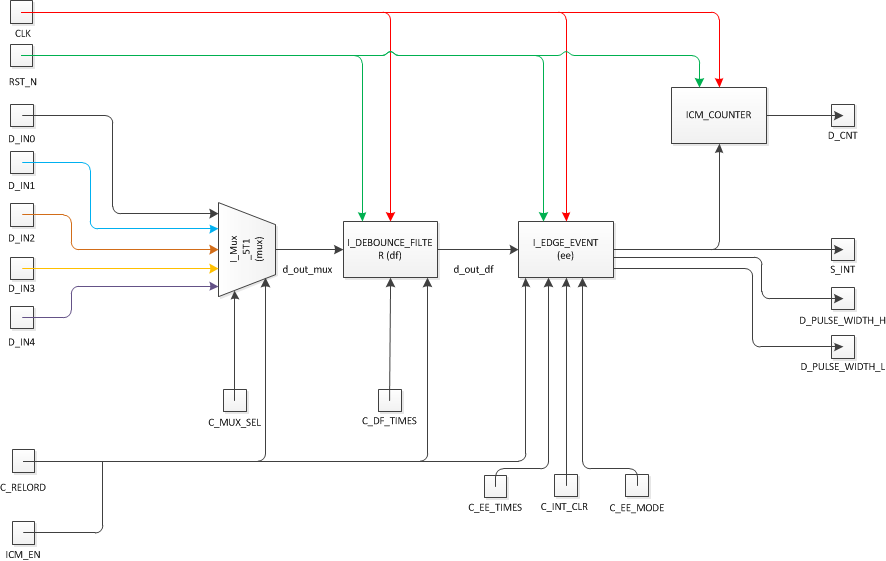
Figure 1011-1 ICM Function Blocks
- I_Mux_5T1: 4 external input signals and 1 internal test signal. Test signal generate from system clock and support to scale the period.
- I_DEBOUNCE_FILTER: Used to filter out noise.
- I_EDGE_EVENT: Three operating modes and all of them can be set event times that decide when to trigger interrupt.
- Rising Edge Detect Mode
- Falling Edge Detect Mode
- Edge Detect Mode
...
11.3 Input Source and Clock
There are 4 input pins and 1 test signal can be selected as input signal source by icm0_mux_sel in ICM0. The icm0_mux_sel is in bit[5:3] of RGST table Group 81.0 icm0_cfg0 register. The ICM0's count clock can be selected by icm0_clk_sel. 4 external clock come from input pins and others source are SYSCLK, 27MHz and 32KHz. The icm0_clk_sel is in bit[8:6] of RGST table Group 81.0 icm0_cfg0 register.
...
11.4 Input Capture Detect Mode
The input capture detect mode of ICM0 can be selected by icm0_ee_mode. The icm0_ee_mode is in bit[1:0] of RGST table Group 81.1 icm0_cfg1 register. Set icm0_ee_mode as 0 for Rising Edge Mode, set icm0_ee_mode as 1 for Falling Edge Mode and set icm0_ee_mode as 2 for Edge Detection Mode. The interrupt trigger timing is controlled by icm0_ee_times. If icm0_ee_times set 7, the interrupt will be triggered after 7 times edge event. The icm0_ee_ times is in bit[5:2] of RGST table Group 81.1 icm0_cfg1 register.
...
11.4.1 Rising Edge Mode
Figure 1011-2 shows the icmx_ee_mode = 0 and icmx_ee_times = 0 or 1 case.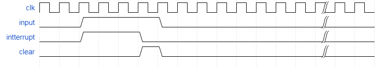
Figure 1011-2 Rising Edge Mode Case1
Figure 1011-3 shows the icmx_ee_mode = 0 and icmx_ee_times = 3 case.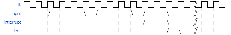
Figure 1011-3 Rising Edge Mode Case2
...
11.4.2 Falling Edge Mode
Figure 1011-4 shows the icmx_ee_mode = 1 and icmx_ee_times = 0 or 1 case.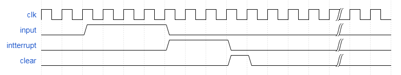
Figure 1011-4 Falling Edge Mode Case1
Figure 1011-5 shows the icmx_ee_mode = 1 and icmx_ee_times = 2 case.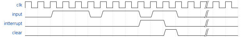
Figure 1011-5 Falling Edge Mode Case2
...
11.4.3 Edge Detection Mode
Figure 1011-6 shows the icmx_ee_mode = 2 and icmx_ee_times = 0 or 1 case.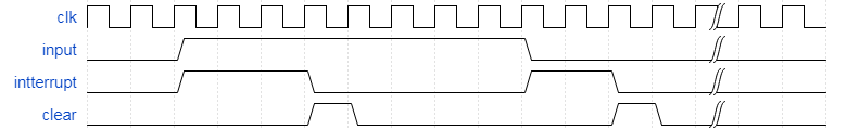
Figure 1011-6 Edge Detection Mode Case1
Figure 1811-7 shows the icmx_ee_mode = 2 and icmx_ee_times = 2 case.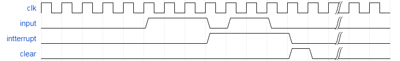
Figure 1011-7 Edge Detection Mode Case2
...
11.5 Interrupt Trigger Counter
The ICM0 interrupt trigger counter value control register is RGST table Group 81.4 icm0_cnt. This register will record the counter value when interrupt happened. This value is updated from FIFO, the FIFO depth is 16. Figure 1011-8 shows the behavior of counter. When interrupt trigger at internal counter 9, the icm0_cnt will be updated to 9 immediately.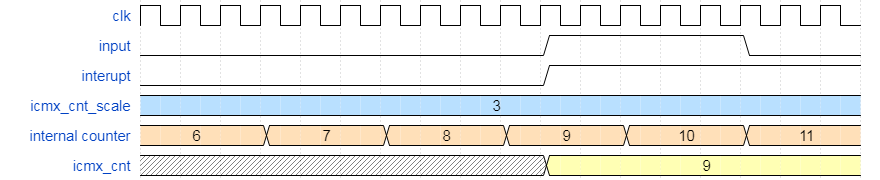
Figure 1011-8 counter behavior
...
11.6 Debounce Filter
The ICM0 debounce filter is controled by icm0_df_times which is bit[8:6] of Group81.1 icm0_cfg1 register. Set the debounce times as 7, the input signals length under 7 clock will be filtered. Figure 1011-9 shows the icm0_df_times=4 case. 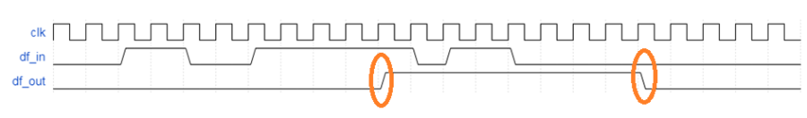
Figure 1011-9 icm0_df_times=4 case
...
11.7 Count Pulse Width H and L
The ICM0 pulse width H and L count value will be recorded in Group 81.5 icm0_pulse_width_h and Group 81.6 icm0_pulse_width_l registers. Figure 1011-10 shows the count pulse width H and L status.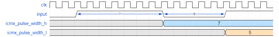
Figure 1011-10 Count Pulse Width H and L
...
11.8 Registers Map
...
11.8.1 Registers Memory Map
Address | Group No. | Register Name | Description |
|---|---|---|---|
0x9C002880 | G81.0 | icm0_cfg0 | ICM0 Config Register 0 |
0x9C002884 | G81.1 | icm0_cfg1 | ICM0 Config Register 1 |
0x9C002888 | G81.2 | icm0_cfg2 | ICM0 Internal Counter Scaler |
0x9C00288C | G81.3 | reserved | reserved |
0x9C002890 | G81.4 | icm0_cnt | ICM0 Interrupt Trigger Counter Value |
0x9C002894 | G81.5 | icm0_pulse_width_h | ICM0 Pulse Width H |
0x9C002898 | G81.6 | icm0_pulse_width_l | ICM0 Pulse Width L |
0x9C00289C | G81.7 | icm1_cfg0 | ICM1 Config Register 0 |
0x9C0028A0 | G81.8 | icm1_cfg1 | ICM1 Config Register 1 |
0x9C0028A4 | G81.9 | icm1_cfg2 | ICM1 Internal Counter Scaler |
0x9C0028A8 | G81.10 | reserved | reserved |
0x9C0028AC | G81.11 | icm1_cnt | ICM1 Interrupt Trigger Counter Value |
0x9C0028B0 | G81.12 | icm1_pulse_witdh_h | ICM1 Pulse Width H |
0x9C0028B4 | G81.13 | icm1_pulse_width_l | ICM1 Pulse Width L |
0x9C0028B8 | G81.14 | icm2_cfg0 | ICM2 Config Register 0 |
0x9C0028BC | G81.15 | icm2_cfg1 | ICM2 Config Register 1 |
0x9C0028C0 | G81.16 | icm2_cfg2 | ICM2 Internal Counter Scaler |
0x9C0028C4 | G81.17 | reserved | reserved |
0x9C0028C8 | G81.18 | icm2_cnt | ICM2 Interrupt Trigger Counter Value |
0x9C0028CC | G81.19 | icm2_pulse_witdh_h | ICM2 Pulse Width H |
0x9C0028D0 | G81.20 | icm2_pulse_width_l | ICM2 Pulse Width L |
0x9C0028D4 | G81.21 | icm3_cfg0 | ICM3 Config Register 0 |
0x9C0028D8 | G81.22 | icm3_cfg1 | ICM3 Config Register 1 |
0x9C0028DC | G81.23 | icm3_cfg2 | ICM3 Internal Counter Scaler |
0x9C0028E0 | G81.24 | reserved | reserved |
0x9C0028E4 | G81.25 | icm3_cnt | ICM3 Interrupt Trigger Counter Value |
0x9C0028E8 | G81.26 | icm3_pulse_witdh_h | ICM3 Pulse Width H |
0x9C0028EC | G81.27 | icm3_pulse_width_l | ICM3 Pulse Width L |
0x9C0028F0 | G81.28 | reserved | reserved |
0x9C0028F4 | G81.29 | reserved | reserved |
0x9C0028F8 | G81.30 | reserved | reserved |
0x9C0028FC | G81.31 | reserved | reserved |
...
11.8.2 Registers Description
RGST Table Group 81 ICM
81.0 ICM0 Config Register 0 (icm0 cfg0)
Address: 0x9C002880
Reset: 0x0000 0000
...