2122.1 Introduction
MMC is the abbreviation of Multi-Media Card. It is a non-volatile memory device that is small in size, large in capacity, low in power consumption, and fast in transmission. It is widely used in consumer electronics.
eMMC is an abbreviation of embedded Multi-Media Card. The embedded memory standard specifications established by the MMC Association are mainly for mobile device products, such as mobile phones...etc. It has been developed on the basis of MMC.
The SD card is a Secure Digital Memory Card, it is also developed on the basis of MMC, adding two main features: SD card emphasizes the security of data, can set the stored usage rights to prevent data from being copied by others; another feature is the transmission speed faster than the MMC2.11 version.
SDIO evolved from SD, emphasizing the interface (IO, Input / Output), no longer pay attention to the specific form of the other end (can be WIFI devices, Bluetooth devices, GPS, etc.).
MMC has evolved different specifications based on different considerations such as MMC, SD, microSD, SDIO, and eMMC. Although the squandering is fascinating, its essence is still the same. This is why the Linux kernel uses the MMC subsystem to manage MMC, SD, SDIO and other devices.
The SP7021 Card Controller (CARD_CTL) supports card type spec reach eMMC4.41, SD2.0 and SDIO2.0.
eMMC supports types that if it's densities < 2G, the block length in 1~512 byte and if it's densities > 2G, the block length is 512 byte. The EMMC supports speed mode include default speed 0~26MHZ, high speed SDR 0~52MHZ and high speed DDR 0~52MHZ. The theoretical speed of data rate is up to 104MB/s.
SD supports SDSC, SDHC and SDXC three types SDcard. The SD/SDIO support speed mode include default speed 0~25MHZ and high speed SDR 0~50MHZ. The theoretical speed of data rate is up to 25MB/s.
The SP7021 card controller control registers locate at RGST table Group118~120 (memory map in 0x9C003B00~0x9C003C7F) for EMMC module, Group125~129 (memory map in 0x9C003E80~0x9C0040FF) for SDCARD module and Group264~268 (memory map in 0x9C008400~0x9C00867F) for SDIO module.
...
22.2 Function Diagram
The SP7021 CARD controller function diagram shows in Figure 2122-1.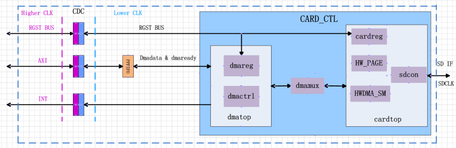
Figure 2122-1 CARD Controller Functional Blocks
- dmatop: This block include dmareg and dmactrl modules. It is responsible for control AXI BUS command and data.
- dmareg: This module control dma register read and write operation.
- dmactrl: This module control AXI BUS command and data response.
- cardtop: This block include cardreg, sdcon, HWDMA_SM and HW_PAGE modules.
- cardreg: This module controls pio mode read and write operations.
- sdcon: This module controls device interface protocol.
- HWDMA_SM: This module controls HW DMA mode read and write operations state machine.
- HW_PAGE: This module controls HW DMA mode sector address/page number and block address/page number update in the read/write operations.
...
22.3 Data Transfer Format
According 1 bit, 4 bit and 8bit mode with trigger in rising edge or both edge, the data transfer have 5 modes. (8 bit mode only be support in EMMC case)
...
22.3.1 1 bit Bus SDR
1 bit Bus SDR (Single Data Rate): The rising edge sampling can be done by simply using one data signal pin (Data 0). Please refer to figure 2122-2.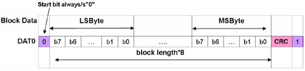
Figure 2122-2 1 bit Bus SDR Data Format
...
22.3.2 4 bit Bus SDR
4 bit Bus SDR: With rising edge sampling, four data signal pins are required (Data 0 ~ Data 3). Please refer to figure 2122-3.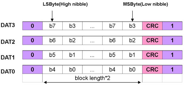
Figure 2122-3 4 bit Bus SDR Data Format
...
22.3.3 8 bit Bus SDR
8 bit Bus SDR: With rising edge sampling, it need to use eight data signal pins (Data 0 ~ Data 7)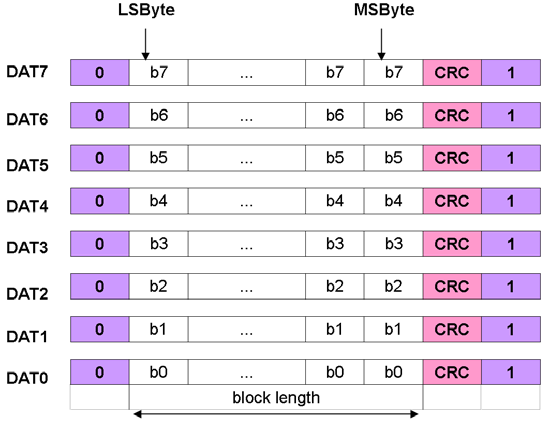
Figure 2122-4 8 bit Bus SDR Data Format
...
22.3.4 4 bit Bus DDR
4 bit Bus DDR (Double Data Rate): Block and CRC are sampled at the rising and falling edges of CLK, while the start and end bits are sampled only at the rising edge. Please refer to figure 2122-4.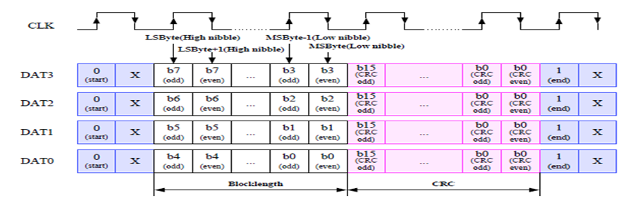
Figure 2122-5 4 bit Bus DDR Data Format
...
22.3.5 8 bit Bus DDR
8 bit Bus DDR (Double Data Rate): Using eight data signal pins (Data 0 ~ Data 7), the data transfer mode is like 4 bit Bus DDR. Please refer to figure 2122-5.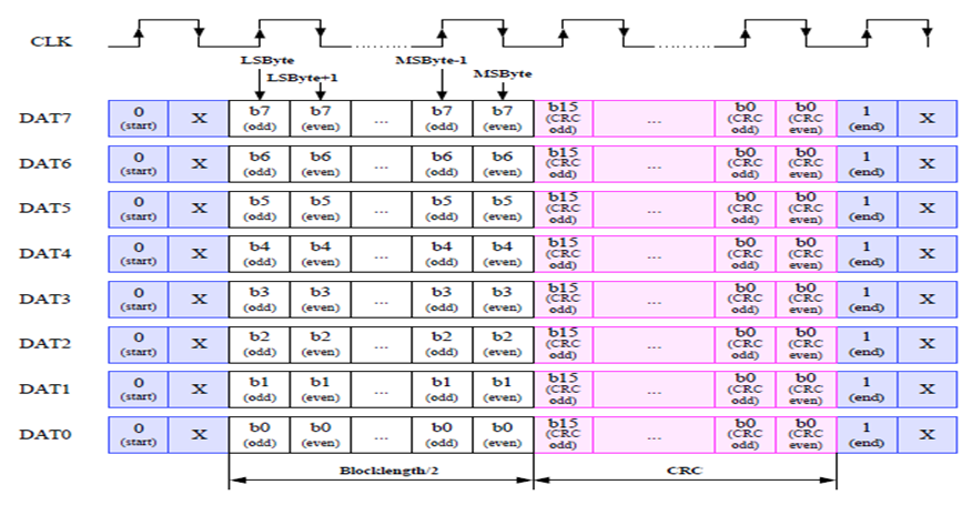
Figure 2122-6 8 bit Bus DDR Data Format
...
22.4 Data Transfer Mode
The EMMC module supports PIO/DMA/HWDMA mode. Please refer to register map chapter for the setting.
The SD/SDIO module only support PIO and DMA mode. Please refer to register map chapter for the setting.
...
22.5 Function Output Port Setting
When the Group1.1 register bit5 set to "1", the EMMC function port will output to SP7021 pin88~97.
When the Group1.1 register bit6 set to "1", the SDCARD function port will output to SP7021 pin81~86.
The SDIO function port can be output to any pins of GPIO port1~8 by set Group2.11~2.13 registers. (Please refer to chapter5 for detail pinmux setting)
...
22.6 Baud Rate Generation
The baud rate setting for EMMC/SD/SDIO modules are SDCLK = DPLL_CLK / (sdfqsel + 1).
The sdfqsel value can be set in Group119.4[31:20], Group126.17[11:0] and Group265.17[11:0] for EMMC, SD and SDIO modules.
...
22.7 Adjust Timing Principle
The basic principle is to offset the latency caused by path delay and device output delay by configuring the three parameters clk_delay, wr_delay, and rd_delay. It should be noted that EMMC/SD/SDIO should distinguish between default speed and high speed during TX operation. When RX is operated, only the SD/SDIO needs to distinguish between default speed and high speed. EMMC does not distinguish between RX and high speed. The adjust timing principle as below description and figure 2122-7&8 show the Default speed SDR mode write and read delay timing status.
- SD/SDIO/EMMC default speed
- write operation(The controller is sent with the negative edge SD_CLK, and the device is sampled using the positive edge SD_CLK)
- When path_clk_delay > path_data_delay, path_data_delay+wr_delay=path_clk_delay
- When path_clk_delay < path_data_delay, path_clk_delay+clk_delay=path_data_delay
- read operation(The controller samples with negative edge SD_CLK, and the device sends with positive edge SD_CLK)
- path_clk_delay + Tout_delay + path_data_delay = rd_delay +SD_CLK/2
- write operation(The controller is sent with the negative edge SD_CLK, and the device is sampled using the positive edge SD_CLK)
- SD/SDIO/EMMC high speed
- write operation(The controller is sent with the positive edge SD_CLK, and the device is sampled with the positive edge SD_CLK)
- path_data_delay+wr_delay=path_clk_delay + SD_CLK/2
- read operation(The controller is sampled with positive edge SD_CLK and the device is sent with positive edge SD_CLK)
- path_clk_delay + Tout_delay + path_data_delay = rd_delay
- write operation(The controller is sent with the positive edge SD_CLK, and the device is sampled with the positive edge SD_CLK)
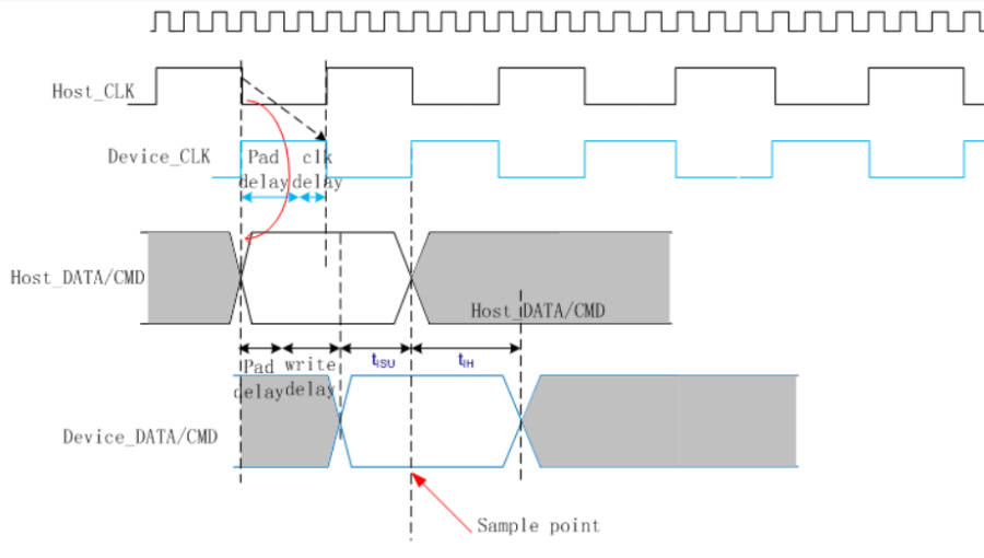
Figure 2122-7 Default speed SDR mode write delay timing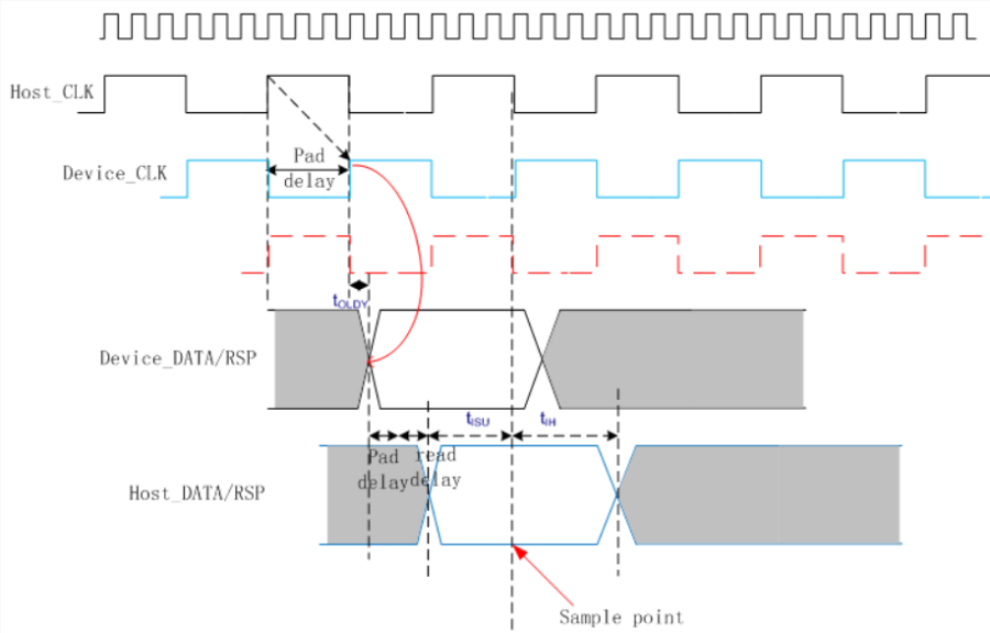
Figure 2122-8 Default speed SDR mode read delay timing
Please refer to register map chapter for the clock/write/read delay timing setting.
...
22.8 CARD_CTL Interrupts
EMMC_CTL support three type interrupts which include pio_int, dma_int and hw_dma _int. SD/SDIO only support two type interrupts which include pio_int and dma_int.
HW DMA can be enable at Group118.4 register bit1. Pio mode and DMA mode can be select at Group119.4 register bit0.
Figure 2122-9 shows the EMMC interrupt tree, figure 2122-10 shows the SD/SDIO interrupt tree. The interrupt status can be read from registers. Please refer to register map chapter. 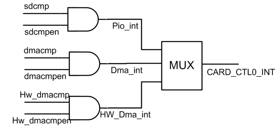
Figure 2122-9 EMMC Interrupt Tree
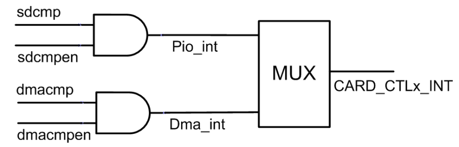
Figure 2122-10 SD/SDIO Interrupt Tree
...
22.9 Register Map
...
22.9.1 Registers Memory Map
CARD0 Register Memory Map
...
CARD1 and CARD4 registers have the same offset in corresponding register group. Only CARD1 registers are described in following register description, for CARD4 please refer to CARD1 description for more detail.
...
22.9.2 Registers Description
RGST Table Group 118 CARD CTL: HW General Config
118.0 Card Media Type And DMA Source/Destination (card mediatype srcdst)
...