2223.1 Introduction
The physical characteristics of Nand Flash make a certain probability of error in the data reading and writing process, so there must be a corresponding error detection and correction mechanism, so the ECC(Error Checking and Correction Code) is used for data error detection and correction. Nand Flash ECC, common algorithms are Hamming code and BCH(Bose–Chaudhuri–Hocquenghem codes). The implementation of such algorithms can be software or hardware. SP7021 implements a hardware BCH for this usage.
The BCH algorithm is usually implemented by the corresponding Nand Flash controller, including the corresponding hardware BCH ECC module, and implements the BCH algorithm. As a software aspect, it is necessary to operate the corresponding BCH-related before reading the data and before writing the data. The register is set to BCH mode, and then the corresponding BCH status register is read to know if there is an error, and the generated BCH check code is used for writing.
The BCH IP is a BCH engine for BCH encode/decode with 14-level BCH algorithms. It can fetch data from system memory for encode/decode and write the result back to the system memory. The Memory is used to storage the data transferred. A NAND device is the data storage unit, which can be accessed by the NAND-Flash controller by a group of signals with proper NAND-Flash interface timing. All the function units communicate through the AXI BUS. Software can select auto encode/decode or manual trigger encode/decode mode.
...
23.2 Function Diagram
A generalized hardware block diagram of BCH is shown in Figure 2223-1.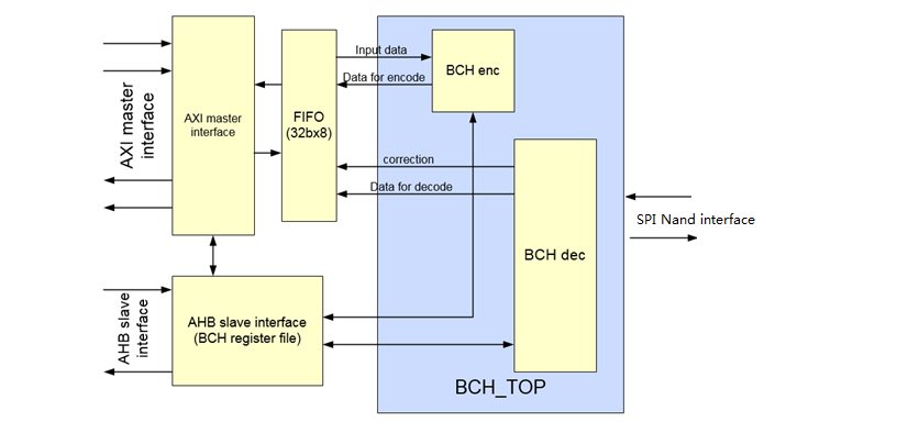
Figure 2223-1 BCH Hardware Block Diagram
- BCH enc: BCH enc is used for BCH encode with 14-level BCH algorithms.
- BCH dec: BCH dec is used for BCH decode with 14-level BCH algorithms.
- AXI master: AXI master is used to transfer data for encode/decode with memory through AXI BUS.
- AHB slave: AHB slave is used to config register file through AHB-lite BUS. CPU can write register in this module through AHB-lite Bus to config function in BCH IP. See the Register chapter for details
...
23.3 Data Structure
Table 2223-1 shows the relationship of ECC data spec, Parity data length and Protect software use byte.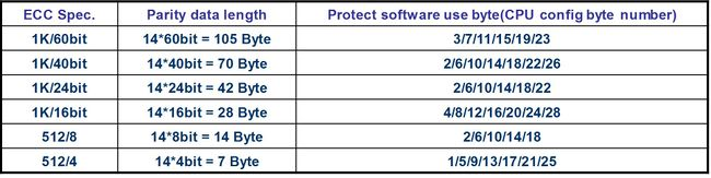
Table 2223-1 ECC Data Format
"1KB/60bit" means the correct ability is 60bit within 1K byte date, "1KB/40bit" means the correct ability is 40bit within 1K byte date and so on.
The sum of the parity and SW protected data must be 4-byte align. The figure 22-2 is the example of ECC spec. as 1K/16b and software protected byte as 4 bytes case.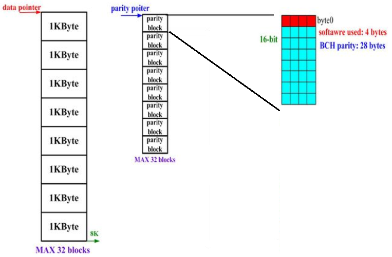
Figure 2223-2 Software Protect Date Size
...
23.4 Auto BCH Enable
Set register Group 87.16 spi_bch bit4 to 1, it will enable auto BCH mode. Please refer to 22.6.2 registers description for more detail description.
...
23.5 BCH Interrupts
There are two kinds of interrupt.
Decode fail Interrupt is issued when bch can't fix data because too much error bits happens and Decode fail mask is true. Finish interrupt is issued when bch work finish and Finish mask is true.
Figure 2223-3 shows the BCH interrupt tree.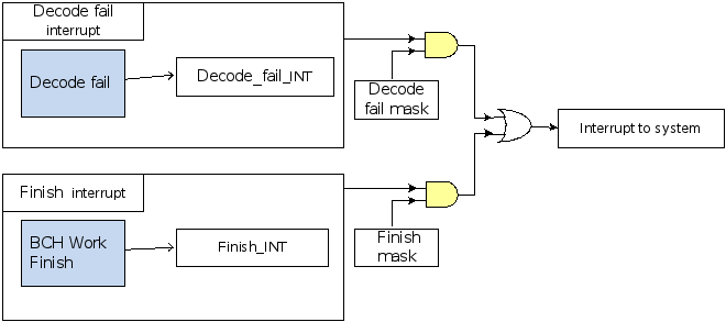
Figure 2223-3 BCH Interrupt Tree
...
23.6 Registers Map
...
23.6.1 Registers Memory Map
BCH Group 0 BCH Controller
Address | Group No. | Register Name | Register Description |
0x9C101000 | G0.0 | configuration | bch control register |
0x9C101004 | G0.1 | data pointer | bch encode/decode data start address |
0x9C101008 | G0.2 | parity pointer | bch encode/decode parity start address |
0x9C10100C | G0.3 | Interrupt status | bch interrupt, write 1 clear |
0x9C101010 | G0.4 | Software clear flag | write 1 to reset bch |
0x9C101014 | G0.5 | Interrupt mask | bch interrupt mask control register |
0x9C101018 | G0.6 | Report status | bch report status |
0x9C10101C | G0.7 | Sector error report | report the Nth (N=0˜31) block has error bit or not |
0x9C101020 | G0.8 | Sector fail report | report the Nth (N=0˜31) block has to much error bits can't be fixed by decoder |
0x9C10102C | G0.11 | Control register | The controller register for ff&00 check and correction method |
...
Address | Group No. | Register Name | Register Description |
| 0x9C002BC0 | G87.16 | spi_bch | SPI BCH configuration Register |
| Anchor | ||||
|---|---|---|---|---|
|
...
23.6.2 Registers Description
BCH Group 0 BCH Controller
0.0 bch control register (configuration)
Address: 0x9C101000
Reset: 0x0
...