10.1 Introduction
The Input Capture Module (ICM) is used to capture a counter value from the ICM's internal counter based upon an event on an input pin. There are four ICM sub modules in the SP7021. The ICM's input source can come from external pins or internal test signal, the counter clock source can also come from external clocks or internal system clock. The ICM features are useful in applications that require frequency (time period) and pulse measurement. The ICM control registers locate at RGST table Group 81.0~31 which memory map in 0x9C002880~0x9C0028FF.
The detail ICM features of the sub module are as below.
- Input source selectable.
- The counter clock source selectable.
- One de-bounce filter
- Three EDGE detect modes and all of them can set event times that decide when to trigger interrupt.
- Report pulse width (high and low) for pulse measurement
- A FIFO buffer (depth is 16) which can record 16 times counter value. User can read from register and the FIFO counter will decrease one. If FIFO is full, the new counter value will be discarded..
Below description will focus on ICM0 , the ICM1/2/3 have the same structure and correspond registers.
10.2 Function Diagram
A generalized function diagram of ICM is shown in Figure 10-1.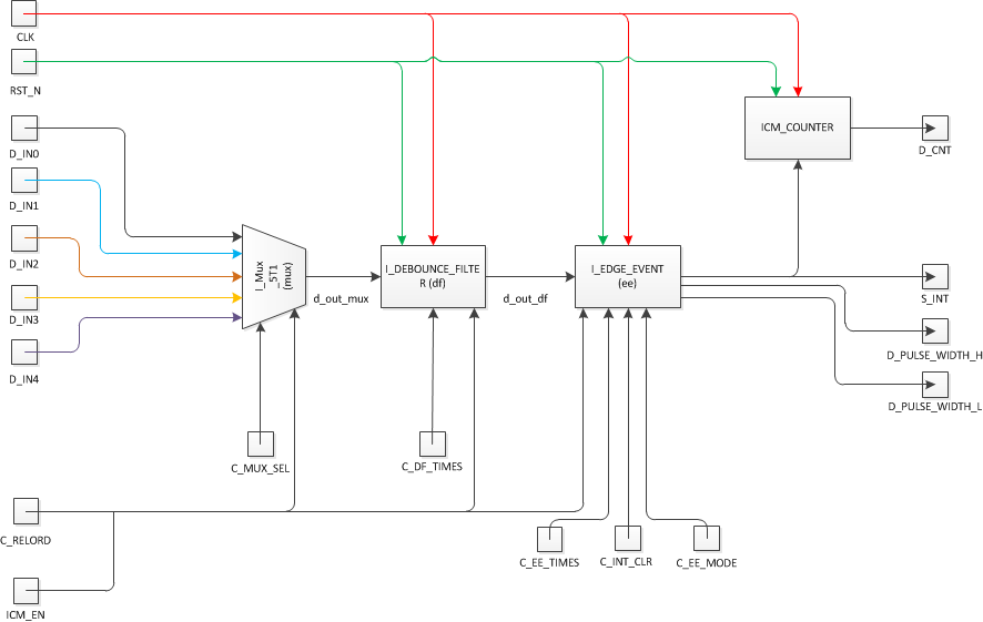
Figure 10-1 ICM Function Blocks
- I_Mux_5T1: 4 external input signals and 1 internal test signal. Test signal generate from system clock and support to scale the period.
- I_DEBOUNCE_FILTER: Used to filter out noise.
- I_EDGE_EVENT: Three operating modes and all of them can be set event times that decide when to trigger interrupt.
- Rising Edge Detect Mode
- Falling Edge Detect Mode
- Edge Detect Mode
10.3 Input Source and Clock
There are 4 input pins and 1 test signal can be selected as input signal source by icm0_mux_sel in ICM0. The icm0_mux_sel is in bit[5:3] of RGST table Group 81.0 icm0_cfg0 register. The ICM0's count clock can be selected by icm0_clk_sel. 4 external clock come from input pins and others source are SYSCLK, 27MHz and 32KHz. The icm0_clk_sel is in bit[8:6] of RGST table Group 81.0 icm0_cfg0 register.
10.4 Input Capture Detect Mode
The input capture detect mode of ICM0 can be selected by icm0_ee_mode. The icm0_ee_mode is in bit[1:0] of RGST table Group 81.1 icm0_cfg1 register. Set icm0_ee_mode as 0 for Rising Edge Mode, set icm0_ee_mode as 1 for Falling Edge Mode and set icm0_ee_mode as 2 for Edge Detection Mode. The interrupt trigger timing is controlled by icm0_ee_times. If icm0_ee_times set 7, the interrupt will be triggered after 7 times edge event. The icm0_ee_ times is in bit[5:2] of RGST table Group 81.1 icm0_cfg1 register.
10.4.1 Rising Edge Mode
Figure 10-2 shows the icmx_ee_mode = 0 and icmx_ee_times = 0 or 1 case.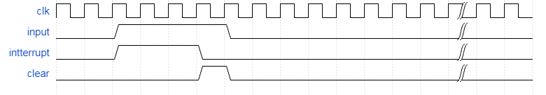
Figure 10-2 Rising Edge Mode Case1
Figure 10-3 shows the icmx_ee_mode = 0 and icmx_ee_times = 3 case.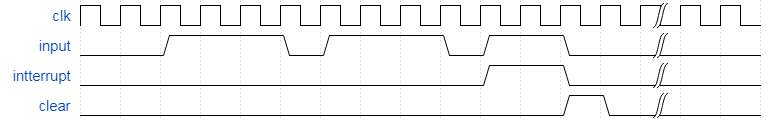
Figure 10-3 Rising Edge Mode Case2
10.4.2 Falling Edge Mode
Figure 10-4 shows the icmx_ee_mode = 1 and icmx_ee_times = 0 or 1 case.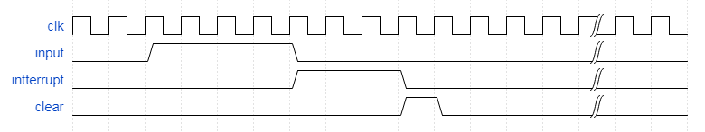
Figure 10-4 Falling Edge Mode Case1
Figure 10-5 shows the icmx_ee_mode = 1 and icmx_ee_times = 2 case.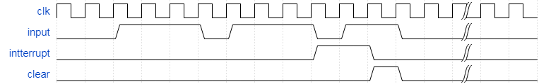
Figure 10-5 Falling Edge Mode Case2
10.4.3 Edge Detection Mode
Figure 10-6 shows the icmx_ee_mode = 2 and icmx_ee_times = 0 or 1 case.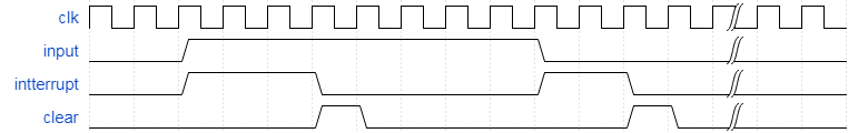
Figure 10-6 Edge Detection Mode Case1
Figure 18-7 shows the icmx_ee_mode = 2 and icmx_ee_times = 2 case.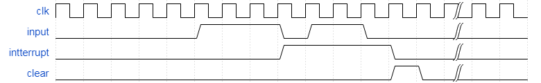
Figure 10-7 Edge Detection Mode Case2
10.5 Interrupt Trigger Counter
The ICM0 interrupt trigger counter value control register is RGST table Group 81.4 icm0_cnt. This register will record the counter value when interrupt happened. This value is updated from FIFO, the FIFO depth is 16. Figure 10-8 shows the behavior of counter. When interrupt trigger at internal counter 9, the icm0_cnt will be updated to 9 immediately.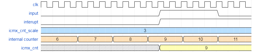
Figure 10-8 counter behavior
10.6 Debounce Filter
The ICM0 debounce filter is controled by icm0_df_times which is bit[8:6] of Group81.1 icm0_cfg1 register. Set the debounce times as 7, the input signals length under 7 clock will be filtered. Figure 10-9 shows the icm0_df_times=4 case. 
Figure 10-9 icm0_df_times=4 case
10.7 Count Pulse Width H and L
The ICM0 pulse width H and L count value will be recorded in Group 81.5 icm0_pulse_width_h and Group 81.6 icm0_pulse_width_l registers. Figure 10-10 shows the count pulse width H and L status.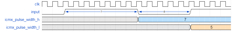
Figure 10-10 Count Pulse Width H and L
10.8 Registers Map
10.8.1 Registers Memory Map
Address | Group No. | Register Name | Description |
|---|---|---|---|
0x9C002880 | G81.0 | icm0_cfg0 | ICM0 Config Register 0 |
0x9C002884 | G81.1 | icm0_cfg1 | ICM0 Config Register 1 |
0x9C002888 | G81.2 | icm0_cfg2 | ICM0 Internal Counter Scaler |
0x9C00288C | G81.3 | icm0_cnt | ICM0 Interrupt Trigger Counter Value |
0x9C002890 | G81.4 | icm0_pulse_witdh_h | ICM0 Pulse Width H |
0x9C002894 | G81.5 | icm0_pulse_width_l | ICM0 Pulse Width L |
0x9C002898 | G81.6 | icm1_cfg0 | ICM1 Config Register 0 |
0x9C00289C | G81.7 | icm1_cfg1 | ICM1 Config Register 1 |
0x9C0028A0 | G81.8 | icm1_cfg2 | ICM1 Internal Counter Scaler |
0x9C0028A4 | G81.9 | icm1_cnt | ICM1 Interrupt Trigger Counter Value |
0x9C0028A8 | G81.10 | icm1_pulse_witdh_h | ICM1 Pulse Width H |
0x9C0028AC | G81.11 | icm1_pulse_width_l | ICM1 Pulse Width L |
0x9C0028B0 | G81.12 | icm2_cfg0 | ICM2 Config Register 0 |
0x9C0028B4 | G81.13 | icm2_cfg1 | ICM2 Config Register 1 |
0x9C0028B8 | G81.14 | icm2_cfg2 | ICM2 Internal Counter Scaler |
0x9C0028BC | G81.15 | icm2_cnt | ICM2 Interrupt Trigger Counter Value |
0x9C0028C0 | G81.16 | icm2_pulse_witdh_h | ICM2 Pulse Width H |
0x9C0028C4 | G81.17 | icm2_pulse_width_l | ICM2 Pulse Width L |
0x9C0028C8 | G81.18 | icm3_cfg0 | ICM3 Config Register 0 |
0x9C0028CC | G81.19 | icm3_cfg1 | ICM3 Config Register 1 |
0x9C0028D0 | G81.20 | icm3_cfg2 | ICM3 Internal Counter Scaler |
0x9C0028D4 | G81.21 | icm3_cnt | ICM3 Interrupt Trigger Counter Value |
0x9C0028D8 | G81.22 | icm3_pulse_witdh_h | ICM3 Pulse Width H |
0x9C0028DC | G81.23 | icm3_pulse_width_l | ICM3 Pulse Width L |
0x9C0028E0 | G81.24 | reserved | reserved |
0x9C0028E4 | G81.25 | reserved | reserved |
0x9C0028E8 | G81.26 | reserved | reserved |
0x9C0028EC | G81.27 | reserved | reserved |
0x9C0028F0 | G81.28 | reserved | reserved |
0x9C0028F4 | G81.29 | reserved | reserved |
0x9C0028F8 | G81.30 | reserved | reserved |
0x9C0028FC | G81.31 | reserved | reserved |
10.8.2 Registers Description
RGST Table Group 81 ICM
81.0 ICM0 Config Register 0 (icm0 cfg0)
Address: 0x9C002880
Reset: 0x0000 0000
| Field Name | Bit | Access | Description |
| Write Mask Bits | 31:16 | RW | Write Mask Bits Example, Intend bit 1 = 1. Set this register 0x00010001 (bit 16 is bit 1 write mask bit). (Example 敘述看不懂) |
| Reserve | 15:9 | RO | |
| icm0 clk sel | 8:6 | RW | ICM0 Clock Source Select (Default value 是哪一個 ? 麻煩在後方註明 (Default)) |
| icm0 mux sel | 5:3 | RW | Select input signal source. 在 7021, 接到 Input 0/1/2/3 的各是什麼信號 ? |
| icm0 int clr | 2 | RW | Clear the interrupt. 有關 Clear 相關的信號, 都要敘述會自行回復 0, 還是軟體要自己寫 0 回復. 如果會自己回復 0, 那這個bit attribute 是 W1C (Write 1 Clear) 而不是 RW |
| Reserve | 1 | RW | Reserved |
| icm0 en | 0 | RW | Input Capture Module 0 Enable 2. Clear the inter- rupt. (2 這句是什麼意思?) |
81.1 ICM0 Config Register 1 (icm0 cfg1)
Address: 0x9C002884
Reset: 0x0000 4000
| Field Name | Bit | Access | Description |
| Write Mask Bits | 31:16 | RW | Write Mask Bits Example, Intend bit 1 = 1. Set this register 0x00010001 (bit 16 is bit 1 write mask bit). (Example 敘述看不懂) |
| icm0 fifo full | 15 | RO | Indicate the fifo is full (fifo depth is 7). 0x0: Non-full 0x1: Full |
| icm0 fifo empty | 14 | RO | Indicate the fifo is empty (fifo depth is 7). 0x0: Non-Empty 0x1: Empty |
| icm0 fifo clr | 13 | RW | Input Capture Module 0 FIFO Clear 0x0: Writing 0 to this bit has no effect 0x1: Clear fifo and icm fifo data drop. (表示 bit 12 會 report status 嗎?) 有關 Clear 相關的信號, 都要敘述會自行回復 0, 還是軟體要自己寫 0 回復. 如果會自己回復 0, 那這個bit attribute 是 W1C (Write 1 Clear) 而不是 RW |
| icm0 fifo data drop | 12 | RO | Input Capture Module 0 Data Dropped 0x0: Non-dropped 0x1: Indicate the fifo data dropped. |
| Reserve | 11:9 | RO | Reserved |
| icm0 df times | 8:6 | RW | Input Capture Module 0 Input Signal Debounce Filter Set the debounce times (0-7) of the input signal de- bounce filter. 0-6 : icm0 df times+1 times, 7:16 times 描述看不懂設定如何對應 debounce 時間, 是 0x0 表示沒有, 0x7 表示敲過7次嗎 ? |
| icm0 ee times | 5:2 | RW | 信號全名 ? Set 0-15. If set 7, intterrupt will be triggered after 8 times edge event. 看不懂敘述 |
| icm0 ee mode | 1:0 | RW | Input capture detect mode Select Others: ? (沒有敘述) |
81.2 ICM0 Internal Counter Scaler (icm0 cfg2)
Address: 0x9C002888
Reset: 0x0000 0000
| Field Name | Bit | Access | Description |
| icm0 cnt scale | 31:0 | RW | Clock prescaler 0-(2ˆ32-1). clk cnt = ext clk / (icmx cnt scale+1) On clk cnt rising edge, (internal counter) = (internal counter) + 1 |
81.3 ICM0 Test Signal Scaler (icm0 cfg3)
Address: 0x9C00288C
Reset: 0x0000 0000
| Field Name | Bit | Access | Description |
| icm0 test sig scale | 31:0 | RW | 信號全名 ? Test signal prescaler 0-(2ˆ32-1). clk test = sysclk / (icmx test sig scale+1) On clk test rising edge, system will generat 1T pulse signal. The Test Signal Period = (icm0 test sig scale+1) + 1, UNIT : T(sysclk) 敘述看不懂 |
81.4 ICM0 Interrupt Trigger Counter Value (icm0 cnt)
Address: 0x9C002890
Reset: 0x0000 0000
| Field Name | Bit | Access | Description |
| icm0 cnt | 31:0 | RO | 信號全名 ? Record the counter value when interrupt happen. Read this from fifo (depth is 15). 意思是說作為 interrupt 發生次數的 counter 嗎 ? 後面那句 read this from FIFO 是什麼意思 ? |
81.5 ICM0 Pulse Width H (icm0 pulse witdh h)
Address: 0x9C002894
Reset: 0x0000 0000
| Field Name | Bit | Access | Description |
| icm0 pulse width h | 31:0 | RO | 信號全名 ? Pulse width : high (unit : t ext clk) 指的是 Positive Pulse 發生次數嗎 ? |
81.6 ICM0 Pulse Width L (icm0 pulse width l)
Address: 0x9C002898
Reset: 0x0000 0000
| Field Name | Bit | Access | Description |
| icm0 pulse width l | 31:0 | RO | 信號全名 ? Pulse width : low (unit : t ext clk) 指的是 Negative Pulse 發生次數嗎 ? |
ICM1 ~ 3 register 的問題與 ICM0 同
81.7 ICM1 Config Register 0 (icm1 cfg0)
Address: 0x9C00289C
Reset: 0x0000 0000
| Field Name | Bit | Access | Description |
| Write Mask Bits | 31:16 | RW | Example, Intend bit 1 = 1. Set this register 0x00010001 (bit 16 is bit 1 write mask bit). |
| Reserve | 15:9 | RO | |
| icm1 clk sel | 8:6 | RW | Select clock source. (External CLK range 32K-210M Hz) 0: External CLK 0 1: External CLK 1 2: External CLK 2 3: External CLK 3 4: SYSCLK 5: 27 MHz 6: 32 KHz Others : 0 |
| icm1 mux sel | 5:3 | RW | Select input signal source. 0: Input 0 1: Input 1 2: Input 2 3: Input 3 4: Test Signal Others: 0 |
| icm1 int clr | 2 | RW | Clear the interrupt. 0: N/A (default) 1: Clear Interrupt |
| Reserve | 1 | RW | |
| icm1 en | 0 | RW | 1. Disable the input capture module. 2. Clear the interrupt. 0: Disable (default) 1: Enable |
81.8 ICM1 Config Register 1 (icm1 cfg1)
Address: 0x9C0028A0
Reset: 0x0000 4000
| Field Name | Bit | Access | Description |
| Write Mask Bits | 31:16 | RW | Example, Intend bit 1 = 1. Set this register 0x00010001 (bit 16 is bit 1 write mask bit). |
| icm1 fifo full | 15 | RO | Indicate the fifo is full (fifo depth is 7). 0: Non-full 1: Full |
| icm1 fifo empty | 14 | RO | Indicate the fifo is empty (fifo depth is 7). 0: Non-mpty 1: Empty |
| icm1 fifo clr | 13 | RW | Clear fifo and icm fifo data drop. |
| icm1 fifo data drop | 12 | RO | Indicate the fifo data droped. |
| Reserve | 11:9 | RO | |
| icm1 df times | 8:6 | RW | Set the debounce times (0-7) of the input signal de- bounce filter. 0-6 : icm0 df times+1 times, 7:16 times |
| icm1 ee times | 5:2 | RW | Set 0-15. If set 7, intterrupt will be triggered after 8 times edge event. |
| icm1 ee mode | 1:0 | RW | Select the input capture detect mode. 0: Rising Edge Mode 1: Falling Edge Mode 2: Edge Detection Mode |
81.9 ICM1 Internal Counter Scaler (icm1 cfg2)
Address: 0x9C0028A4
Reset: 0x0000 0000
| Field Name | Bit | Access | Description |
| icm1 cnt scale | 31:0 | RW | Clock prescaler 0-(2ˆ32-1). clk cnt = ext clk / (icmx cnt scale+1) On clk cnt rising edge, (internal counter) = (internal counter) + 1 |
81.10 ICM1 Test Signal Scaler (icm1 cfg3)
Address: 0x9C0028A8
Reset: 0x0000 0000
| Field Name | Bit | Access | Description |
| icm1 test sig scale | 31:0 | RW | Test signal prescaler 0-(2ˆ32-1). clk test = sysclk / (icmx test sig scale+1) On clk test rising edge, system will generat 1T pulse signal. The Test Signal Period = (icm0 test sig scale+1) + 1, UNIT : T(sysclk) |
81.11 ICM1 Interrupt Trigger Counter Value (icm1 cnt)
Address: 0x9C0028AC
Reset: 0x0000 0000
| Field Name | Bit | Access | Description |
| icm1 cnt | 31:0 | RO | Record the counter value when interrupt happen. Read this from fifo (depth is 15). |
81.12 ICM1 Pulse Width H (icm1 pulse witdh h)
Address: 0x9C0028B0
Reset: 0x0000 0000
| Field Name | Bit | Access | Description |
| icm1 pulse width h | 31:0 | RO | Pulse width : high (unit : t ext clk) |
81.13 ICM1 Pulse Width L (icm1 pulse width l)
Address: 0x9C0028B4
Reset: 0x0000 0000
| Field Name | Bit | Access | Description |
| icm1 pulse width l | 31:0 | RO | Pulse width : low (unit : t ext clk) |
81.14 ICM2 Config Register 0 (icm2 cfg0)
Address: 0x9C0028B8
Reset: 0x0000 0000
| Field Name | Bit | Access | Description |
| Write Mask Bits | 31:16 | RW | Example, Intend bit 1 = 1. Set this register 0x00010001 (bit 16 is bit 1 write mask bit). |
| Reserve | 15:9 | RO | |
| icm2 clk sel | 8:6 | RW | Select clock source. (External CLK range 32K-210M Hz) 0: External CLK 0 1: External CLK 1 2: External CLK 2 3: External CLK 3 4: SYSCLK 5: 27 MHz 6: 32 KHz Others : 0 |
| icm2 mux sel | 5:3 | RW | Selec input signal source. 0: Input 0 1: Input 1 2: Input 2 3: Input 3 4: Test Signal Others: 0 |
| icm2 int clr | 2 | RW | Clear the interrupt. 0: N/A (default) 1: Clear Interrupt |
| Reserve | 1 | RW | |
| icm2 en | 0 | RW | 1. Disable the input capture module. 2. Clear the inter- rupt. 0: Disable (default) 1: Enable |
81.15 ICM2 Config Register 1 (icm2 cfg1)
Address: 0x9C0028BC
Reset: 0x0000 4000
| Field Name | Bit | Access | Description |
| Write Mask Bits | 31:16 | RW | Example, Intend bit 1 = 1. Set this register 0x00010001 (bit 16 is bit 1 write mask bit). |
| icm2 fifo full | 15 | RO | Indicate the fifo is full (fifo depth is 7). 0: Non-full 1: Full |
| icm2 fifo empty | 14 | RO | Indicate the fifo is empty (fifo depth is 7). 0: Non-mpty 1: Empty |
| icm2 fifo clr | 13 | RW | Clear fifo |
| icm2 fifo data drop | 12 | RO | Clear fifo and icm fifo data drop. |
| Reserve | 11:9 | RO | |
| icm2 df times | 8:6 | RW | Set the debounce times (0-7) of the input signal de- bounce filter. 0-6 : icm0 df times+1 times, 7:16 times |
icm2 ee times | 5:2 | RW | Set 0-15. If set 7, intterrupt will be triggered after 8 times edge event. |
|
|
|
|
81.16 ICM2 Internal Counter Scaler (icm2 cfg2)
Address: 0x9C0028C0
Reset: 0x0000 0000
| Field Name | Bit | Access | Description |
| icm2 cnt scale | 31:0 | RW | Clock prescaler 0-(2ˆ32-1). clk cnt = ext clk / (icmx cnt scale+1) On clk cnt rising edge, (internal counter) = (internal counter) + 1 |
81.17 ICM2 Test Signal Scaler (icm2 cfg3)
Address: 0x9C0028C4
Reset: 0x0000 0000
| Field Name | Bit | Access | Description |
| icm2 test sig scale | 31:0 | RW | Test signal prescaler 0-(2ˆ32-1). clk test = sysclk / (icmx test sig scale+1) On clk test rising edge, system will generat 1T pulse signal. The Test Signal Period = (icm0 test sig scale+1) + 1, UNIT : T(sysclk) |
81.18 ICM2 Interrupt Trigger Counter Value (icm2 cnt)
Address: 0x9C0028C8
Reset: 0x0000 0000
| Field Name | Bit | Access | Description |
| icm2 cnt | 31:0 | RO | Record the counter value when interrupt happen. Read this from fifo (depth is 15). |
81.19 ICM2 Pulse Width H (icm2 pulse witdh h)
Address: 0x9C0028CC
Reset: 0x0000 0000
| Field Name | Bit | Access | Description |
| icm2 pulse width h | 31:0 | RO | Pulse width : high (unit : t ext clk) |
81.20 ICM2 Pulse Width L (icm2 pulse width l)
Address: 0x9C0028D0
Reset: 0x0000 0000
| Field Name | Bit | Access | Description |
| icm2 pulse width l | 31:0 | RO | Pulse width : low (unit : t ext clk) |
81.21 ICM3 Config Register 0 (icm3 cfg0)
Address: 0x9C0028D4
Reset: 0x0000 0000
| Field Name | Bit | Access | Description |
| Write Mask Bits | 31:16 | RW | Example, Intend bit 1 = 1. Set this register 0x00010001 (bit 16 is bit 1 write mask bit). |
| Reserve | 15:9 | RO | |
| icm3 clk sel | 8:6 | RW | Select clock source. (External CLK range 32K-210M Hz) 0: External CLK 0 1: External CLK 1 2: External CLK 2 3: External CLK 3 4: SYSCLK 5: 27 MHz 6: 32 KHz Others : 0 |
| icm3 mux sel | 5:3 | RW | Select input signal source. 0: Input 0 1: Input 1 2: Input 2 3: Input 3 4: Test Signal Others: 0 |
| icm3 int clr | 2 | RW | Clear the interrupt. 0: N/A (default) 1: Clear Interrupt |
| Reserve | 1 | RW | |
| icm3 en | 0 | RW | 1. Disable the input capture module. 2. Clear the inter- rupt. 0: Disable 1: Enable (default) |
81.22 ICM3 Config Register 1 (icm3 cfg1)
Address: 0x9C0028D8
Reset: 0x0000 4000
| Field Name | Bit | Access | Description |
| Write Mask Bits | 31:16 | RW | Example, Intend bit 1 = 1. Set this register 0x00010001 (bit 16 is bit 1 write mask bit). |
| icm3 fifo full | 15 | RO | Indicate the fifo is full (fifo depth is 7). 0: Non-full 1: Full |
| icm3 fifo empty | 14 | RO | Indicate the fifo is empty (fifo depth is 7). 0: Non-mpty 1: Empty |
icm3 fifo clr | 13 | RW | Clear fifo and icm fifo data drop. |
|
|
|
|
|
|
| |
|
|
|
|
|
|
|
|
|
|
|
|
81.23 ICM3 Internal Counter Scaler (icm3 cfg2)
Address: 0x9C0028DC
Reset: 0x0000 0000
| Field Name | Bit | Access | Description |
| icm3 cnt scale | 31:0 | RW | Clock prescaler 0-(2ˆ32-1). clk cnt = ext clk / (icmx cnt scale+1) On clk cnt rising edge, (internal counter) = (internal counter) + 1 |
81.24 ICM3 Test Signal Scaler (icm3 cfg3)
Address: 0x9C0028E0
Reset: 0x0000 0000
| Field Name | Bit | Access | Description |
| icm3 test sig scale | 31:0 | RW | Test signal prescaler 0-(2ˆ32-1). clk test = sysclk / (icmx test sig scale+1) On clk test rising edge, system will generat 1T pulse signal. The Test Signal Period = (icm0 test sig scale+1) + 1, UNIT : T(sysclk) |
81.25 ICM3 Interrupt Trigger Counter Value (icm3 cnt)
Address: 0x9C0028E4
Reset: 0x0000 0000
| Field Name | Bit | Access | Description |
| icm3 cnt | 31:0 | RO | Record the counter value when interrupt happen. Read this from fifo (depth is 15). |
81.26 ICM3 Pulse Width H (icm3 pulse witdh h)
Address: 0x9C0028E8
Reset: 0x0000 0000
| Field Name | Bit | Access | Description |
| icm3 pulse width h | 31:0 | RO | Pulse width : high (unit : t ext clk) |
81.27 ICM3 Pulse Width L (icm3 pulse width l)
Address: 0x9C0028EC
Reset: 0x0000 0000
Field Name | Bit | Access | Description |
icm3 pulse width l | 31:0 | RO | Pulse width : low (unit : t ext clk) |
81.28 (Reserved)
Address: 0x9C0028F0
Reset: 0x0000 0000
Field Name | Bit | Access | Description |
Reserved | 31:0 | RO |
81.29 (Reserved)
Address: 0x9C0028F4
Reset: 0x0000 0000
Field Name | Bit | Access | Description |
Reserved | 31:0 | RO |
81.30 (Reserved)
Address:0x9C0028F8
Reset: 0x0000 0000
Field Name | Bit | Access | Description |
Reserved | 31:0 | RO | Reserved |
81.31 IP Version (ip version)
Address: 0x9C0028FC
Reset: 0x1811 1001
Field Name | Bit | Access | Description |
| ip version | 31:0 | RO | IP Version 0xaabbcdee, a : year (eg 0X018) b : month (BCD : 01-12) c |