Nor FLASH is easy to use, easy to connect, can run code directly on the chip, and has excellent stability, high transfer rate, and high cost performance in small capacity, which makes it suitable for FLASH ROM in embedded systems. SPI NOR FLASH, the host and the flash chip communicate using the SPI (Serial Peripheral Interface) bus.
The SP7021 SPI_NOR Controller is used to transmit or receive data with SPI_NOR device. It supports the following functions:
Support 1 byte length or skip command bits
Address Bytes
Support 1/2/4 bit transferred mode
Support 1/2/3 byte length or skip address bits
Support 2/4/6/8/16/32 dummy cycles or skip dummy cycles
Data Bytes
Support 1/2/4 bit transferred mode
Support 1 - 65535 byte length or skip
Compared to NOR FLASH, NAND FLASH emphasizes higher performance, lower cost, smaller size and longer life. This makes NAND FLASH very good at storing pure data or data, etc., used to support file system in embedded systems. SPI NAND FLASH, the host and the flash chip communicate using the SPI (Serial Peripheral Interface) bus.
SP7021 SPI_NAND Controller is used to transmit or receive data with SPI_NAND device. It supports the following functions:
Command Byte
Support 1/2/4 bit transferred mode
Support 1 byte length or skip command bits
Address Bytes
Support 1/2/4 bit transferred mode
Support 1/2/3 byte length or skip address bits
Support 2/4/6/8/16/32 dummy cycles or skip dummy cycles
Data Bytes
Support 1/2/4 bit transferred mode
Support 1 - 65535 byte length or skip data bits
SPI Device Number
Support 1 or 2 SPI chips
Support configurable chip selected, command should be valid only relative chip selected.
Support BCH auto encode and decode
Support 32-bit AXI master bus for transferring data between controller and dram for DMA mode
Exchange to 32-bit AXI Slave bus from 32-bit OCP bus
Support auto multi page read
Support auto multi page program
Support enable BCH function for DMA mode
Support SPI_CLK is divided from CLK_SPI, and frequency division coefficient is 1/2, 1/4, 1/6, 1/8, 1/16, 1/24, 1/32
eMMC is a standard embedded memory standard established by the MMCA Association (Multi Media Card Association). It is mainly for mobile phone products, simplifying the design of memory, and using NAND FLASH chip and control in multi-chip package (MCP). The chip is packaged into a single chip, which eliminates the area occupied by components and the board. The eMMC can be said to be an embedded MMC specification interface product.
The SP7021 eMMC Controller is used to transmit or receive data with eMMC device. It supports the following functions:
eMMC controller, used for primary boot disk, supports eMMC 4.41 DDR 104MB/s speed mode.
EMMC Speed Mode
Default speed (26MHz)
High speed SDR mode (52MHz)
High speed DDR mode (52MHz)
Support Card Bit Mode
1 bit、4 bit、8 bit
Support Timing Adjustment
clock auto adjustment
write auto adjustment
read auto adjustment
Support Data Transfer Mode
EMMC PIO/DMA/HW DMA mode
Single/Multiple block read/write
The SD controller, used for removable media, the SDIO controller, used for Wi-Fi module, both support reach SDIO 2.0 SDR 25MB/s speed mode.
Support SDIO 2.0
Support Card Capacity
Support SDHC and SDXC
Support Card Speed Mode
SDIO Speed Mode
Support Default speed(25MHz)
Support High speed SDR mode(50MHz)
Support Card Bit Mode
Support 1 bit、4 bits
Support Timing Adjustment
Support clock auto adjustment
Support write auto adjustment
Support read auto adjustment
Adjustment range is 1~7 DPLL clock cycle
Support Data Transfer Mode
Support SDIO/SD PIO/DMA mode
Support Single/Multiple block read/write
I²C is invented by Philips Semiconductor and typically used for attaching lower-speed peripheral ICs communication. Two bus lines are required: a serial data line(SDA) and a serial clock line(SCL). There are four I²C master devices in SP7021 , they support the following functions:
Support Standard-mode (100KHz) and Fast-mode (400KHz)
Buffer depth reach FIFO 32
Support Read Mode, Write Mode and Restart Mode
Support DMA function
The SPI is Serial Peripheral Interface Bus, similar to I²C, is a 4-wire synchronous serial data protocol for portable device platform systems. SPI is a synchronous-based full-duplex master-slave interface. Data from the master or slave is synchronized on the rising or falling edge of the clock. Both master and slave can transfer data simultaneously.
UART is Universal Asynchronous Receiver/Transmitter, the interface is EIA RS-232C DB-9. Transmitting and receiving data at the same time. There are five UART devices in SP7021 , they support the following functions:
FIFO depth: 128 byte
The internal loop-back capability allows on-board diagnostics
The Input Capture module (ICM) is used to capture a counter value from the ICM’s internal counter based upon an event on an input pin. The ICM features are useful in applications that require frequency (time period) and pulse measurement.
The ICM includes four sub module in SP7021 and the detail features of the sub module as below.
5 to 1 input signal MUX. 4 external input signal and 1 internal test signal. Test signal generate from system clock and support to scale the period.
One de-bounce filter
Three operating modes and all of them can set event times that decide when to trigger interrupt.
Rising Edge Detect Mode
Falling Edge Detect Mode
Edge Detect Mode
Report pulse width (high and low) for pulse measurement
A FIFO buffer (depth is 16) which can record 16 times counter value. User can read from register and the FIFO counter will be decreased by one. If FIFO is full, the new counter value will be discarded.
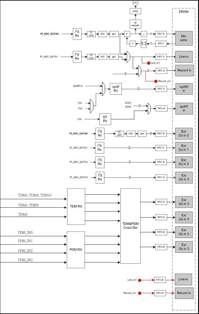
Audio IN interface contains the standard I2S and S/PDIF interface, signal recording from ADC, and multi-channel mix. It supports up to 192KHz sample rate. It can also decode the I2s or SPDIF signal and save the data in DRAM for further usage.

Figure 6-1 Audio In Block Diagram
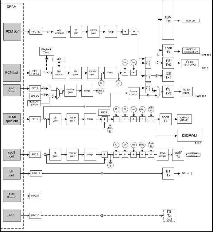
When the audio data has been decoded and saved in DRAM, Audio module will fetch the data from DRAM and encode it with I2S or SPDIF protocol.

Figure 6-2 Audio Out Block Diagram
TTL interface timing supports 320x240 and RGB888 outputs, 2 simple functions, RGB side reverse and RGB channel switching.
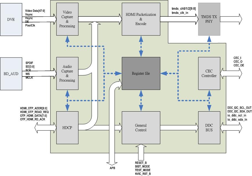
HDMI stands for "High Definition Multimedia Interface" to transmit high quality video and audio in a single cable. The HDMI TX IP is composed of video, audio and HDCP cipher engine and intends to be integrated to a SoC to deliver high quality video and audio over a single cable.

Figure 6-3 HDMI Block Diagram
The Real Time Clock (RTC) is a feature that can keep counting the time using external back-up battery when main system power-off. In this design a 32-bits counter is implemented for time in seconds. The conversion from second to time and date is calculated by software.
This design also provides an alarm feature that can be used to allow main system to 'wake up' after shut down to execute tasks in a certain moment. The alarm setting in seconds, the conversion from to time and date to second is calculated by software.
Back-up power source can used A Super Cap or a coin battery (like CR2032), and build-in charging circuit without any external component.
Associated control registers locate in Group116.0~31 which memory map to 9C003A00h-9C003A7Ch.