30.1 Introduction
...
- MST_CORE: Receive or transmit data from or to SPI_SLAVE
- DMA_CTRL_W: Receive DATA from MST_CORE and produce WDATA_REQ with transmit 4-byte data to DMA_LINK_W
- DMA_CTRL_R: Transmit DATA to MST_CORE and produce RDATA_REQ with receive 4-byte data from DMA_LINK_R
- DMA_LINK_R/W: Communicate with DMA_CTRL via proprietary System Bus (SBUS) protocol
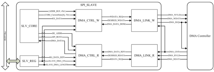
Figure 30-4 SPI Slave DMA Function Block
...
30.15.2 Registers Description
| Anchor | ||||
|---|---|---|---|---|
|
SPI Register Description
RGST Table Group 91 SPI MASTER 0
...
Field Name | Bit | Access | Description |
REG_TOTAL_LENGTH_FD | 31:24 | RW | Total length for full duplex |
REG_TX_LENGTH_FD | 23:16 | RW | TX length for full duplex max 255 byte,less than total length |
REG_RX_CNT | 15:12 | RO | RX FIFO CNT for full duplex 0 with empty signal - 0byte, 1 - 1byte, 0 with full signal - 16byte |
REG_TX_CNT | 11:8 | RO | TX FIFO CNT for full duplex 0 with empty signal - 0byte, 1 - 1byte, 0 with full signal - 16byte |
REG_SPI_BUSY_FD | 7 | RO | SPI_BUSY for full duplex 1 - : idle |
REG_FINISH_FLAG | 6 | WO | FINISH_FLAG for full duplex |
REG_RX_FUL_FLAG | 5 | RO | RX_FIFO_FUL_FLAG for full duplex |
REG_RX_EMP_FLAG | 4 | RO | RX_FIFO_EMP_FLAG for full duplex |
REG_TX_FUL_FLAG | 3 | RO | TX_FIFO_FUL_FLAG for full duplex |
REG_TX_EMP_FLAG | 2 | RO | TX_FIFO_EMP_FLAG for full duplex |
REG_MASTER_SW_RST | 1 | RO | SW RST for full duplex |
REG_SPI_START_FD | 0 | RO | SPI START for full duplex |
...
Field Name | Bit | Access | Description |
REG_SPI_CLK_CNT_FD | 31:16 | RW | Ratio between SPI clk and sysclk |
REG_FINISH_MASK | 15 | RW | FINISH_MASK for full duplex |
REG_RX_FUL_MASK | 14 | RW | RX_FIFO_FUL_MASK for full duplex |
REG_RX_EMP_MASK | 13 | RW | RX_FIFO_EMP_MASK for full duplex |
REG_TX_FUL_MASK | 12 | RW | TX_FIFO_FUL_MASK for full duplex |
REG_TX_EMP_MASK | 11 | RW | TX_FIFO_EMP_MASK for full duplex |
REG_WRITE_BYTE | 10:9 | RW | WRITE_BYTE for full duplex |
REG_READ_BYTE | 8:7 | RW | READ_BYTE for full duplex |
REG_HALF_FULL_SEL | 6 | RO | HALF_FULL_SEL for full duplex 1 - : full duplex mode |
REG_EN_POR_FD | 5 | RW | EN POLARITY for full duplex 1 - : cs hign acitve |
REG_LSB_SEL_FD | 4 | RW | LSB SELECT for full duplex 1 - : lsb |
REG_DELAY_FD | 3 | RW | DEALY ENABLE IN RX for full duplex |
REG_CPHA_W_FD | 2 | RW | CPHA_W TX for full duplex 1: second edge launch ; 0 - first edge launch |
REG_CPHA_R_FD | 1 | RW | CPHA_R RX for full duplex 1 - : second edge capture ; 0 - first edge capture |
REG_CPOL_FD | 0 | RW | CPOL for full duplex |
...
1: clk high when idle |
91.17 SPI master control and clock select register (spi ctrl clk sel)
...
Field Name | Bit | Access | Description |
R DLY | 31:30 | RW | Additional delay in read action 0x0: No delay(default) 0x1: Delay 0.5*SPI clk cycle0x2cycle 0x2: Delay 1*SPI clk cycle0x3cycle 0x3: Delay 1.5*SPI clk cycle |
SPI CLOCK SEL | 29:16 | RW | Ratio between SPI clk and sysclk1/(2*(CLK SEL+1)) |
Reserve | 15:9 | RW | Reserved |
ADDR BIT NUM | 8:7 | RW | Transfer address bit number 0x0: 12-bit0x1bit 0x1: 12-bit0x2bit 0x2: 16-bit0x3bit 0x3: 20-bit |
WRITE SAMPLING EDGE | 6 | RW | SPI TX edge 1: Falling edge of SPI clk |
READ SAMPLING EDGE | 5 | RW | SPI RX edge 1: Falling edge of SPI clk |
EN POLARITY | 4 | RW | SPI CS polarity 1: High active |
READ POLARITY | 3 | RW | Read/Write bit polarity 1: Low read |
RW POSITION | 2 | RW | Read/Write bit position 1: Addr[7] is R/W bit |
SB SELECT | 1 | RW | LSB enable in SPI transmission 1: Begin at bit7 |
SPISTART | 1 | WO | SPI transmission start It will return to 0 automatically when SPI transmission finish. |
...
Field Name | Bit | Access | Description |
Reserve | 31:5 | RO | Reserved |
BYTE NO | 4:0 | RW | No. of bytes in SPI transmission Support from 1-byte to 16-byte |
...
Field Name | Bit | Access | Description |
Reserve | 31:10 | RO | RESERVED |
PI BUSY FLAG | 9 | RO | Indicator of BUSY signal from TI2046 chip |
PI BUSY EN | 8 | RO | Support TI2046 BUSY signal Return data is valid when busy signal is low afterSPI after SPI MASTER issues command. 0: Disable(default) 1: Enable |
MASTER INT STATUS | 7 | RO | Master interrupt to RISC |
MASTER INT CLR | 6 | RW | Master INT clear 1: Clear SPI master interruptit interrupt It will return to 0 automatically when interrupt is low. |
REG INT EDGE | 5 | RW | Define incoming SPI interrupt trigger polarity 0: low level or falling edge interrupt1interrupt 1: high level or rising edge interrupt(default) |
REG INT TYPE | 4 | RW | Define incoming SPI interrupt trigger type 0: level interrupt(default) 1: edge interrupt |
REG INT BYPASS | 3 | RW | SPI master INT bypass 0: SPI master INT comes from SPI master module(default) 1: SPI master INT comes direct from incoming SPI interrupt |
REG INT TIMEOUT | 2 | RW | SPI master INT timeout function SPI master module will launch SPI master INT again when CPU has served INT but the incoming SPI interrupt is still in active state. 0: Disable(default) 1: Enable |
RW PHASE | 1 | RO | Indicator of SPI write/ read action 0: read(default) 1: write |
REG SPI BUSY | 0 | RO | Indicator of SPI master operation status 0: SPI master is not in operation(default) 1: SPI master is in operation: BUSY. |
...
Field Name | Bit | Access | Description |
Reserve | 31:9 | RO | RESERVED |
DMA W INT STATUS | 8 | RO | DMA Write interrupt status Whether DMA transmission is finished or not. |
DMA W INT CLR | 7 | RW | DMA Write interrupt clear 1: Clear DMA write interruptit interrupt It will return to 0 automatically when interrupt is low. |
DMA RW SEL | 6 | RW | DMA read/write select 0: DMA write to DRAM(default) 1: DMA read from DRAM MASTER |
DMA BANK | 5 | RW | DRAM bank select 0x0: Bank A(default) 0x1: Bank B |
MASTER DMA BP WBE | 4 | RWRW | SBUS write-byte enable select 0: With write-byte-enable(default) 1: No write-byte-enable Used in Legacy SBUS protocol, not supported any more. Left default value without change. |
MASTER DMA BURST | 3:2 | SBUS command select 0x0: 4 bytes command(default) 0x1: 8 bytes command0x3command 0x3: A4B4 command others: reserved | |
MASTER MASTER SW RST | 1 | RW | SPI master software reset 0: Disable(default) 1: Enable |
MASTER DMA EN | 0 | RW | DMA function select 0: Disable(default) 1: Enable |
91.21 SPI master DMA length register (master dma length)
...
Field Name | Bit | Access | Description |
DMA ADDR STATUS | 31:0 | RO | DMA address status Return address which DMA access |
...
Field Name | Bit | Access | Description |
Reserve | 31:3 | RO | RESERVED |
UART SW RST | 2 | RW | Software reset when SPI in UART DMA mode |
UART DMA START | 1 | W1C | DMA transmission start signal from UART 1: DMA transmission start ; it will return to 0 automatically. |
UART DMA EN | 0 | RW | DMA function select from UART 0: Disable(default) 1: Enable |
91.28 Reserved (reserved)
...
Field Name | Bit | Access | Description |
Reserve | 31:4 | RO | RESERVED |
SPI EXTRA CYCLE | 3:2 | RW | Choose the number of SPI extra cycle. These settings take effect ONLY when SPI EXTRA CYCLE EN=1'b1 0x0: Add extra 1 SPI cycle(default) 0x1: Add extra 2 SPI cycle 0x2: Add extra 3 SPI cycle 0x3: Add extra 4 SPI cycle |
SPI EN CUT | 1 | RW | SPI EN output interval selectThis select This setting takes effect ONLY when SPI EXTRA CYCLE EN=1'b1 0: SPI EN output interval will be SPI read plus SPI extra cycle.(default) 1: SPI EN output interval will be as same as SPI read. |
SPI EXTRA CYCLE EN | 0 | RW | Enable SPI extra cycle to fixpath fix path delay in SPI read pro- cess process 0: Disable(default) 1: Enable |
91.31DMA data ready register (dma data ready)
...
Field Name | Bit | Access | Description |
Reserve | 31:1 | RO | RESERVED |
MST DMA DATA RDY | 0 | RO | DMA Read data pre-fetch prefetch ready |
RGST Table Group 92 SPI SLAVE0
...
Field Name | Bit | Access | Description |
RESERVED | 31:10 | RO | RESERVED |
SPI SLAVE INT | 9 | RO | SPI Slave Interrupt Register SPI slave will launch INT to CPU when SPI transmission is finished no matter write or read action. |
SLAVE INT CLR | 8 | RW | SPI slave INT clear 1: Clear SPI slave interruptit will return to 0 automatically when interrupt is low. |
RESERVED | 7:1 | RO | RESERVED |
SLAVE DATA RDY | 0 | RW | SPI slave data ready signal 1: SPI slave data is ready and launch INT to SPI master. It will return to 0 automatically. |
...
Field Name | Bit | Access | Description |
RESERVED | 31:7 | RO | RESERVED |
SLAVE DMA RW SEL | 6 | RW | SLAVE DMA read/write select 0: DMA write to DRAM(default) 1: DMA read from DRAM |
SLAVE DMA BANK | 5 | RW | DRAM bank select 0 0: Bank A(default) 1: Bank B |
SLAVE DMA BP WBE | 4 | RW | SBUS write-byte enable select 0: With write-byte-enable(default) 1: No write-byte-enable |
SLAVE DMA BURST | 3:2 | RW | SBUS command select 0x0: 4 bytes command(default) 0x1: 8 bytes command 0x3: A4B4 command |
SLAVE SLAVE SW RST | 1 | RW | SPI slave software reset 0: Disable(default) 1: Enable |
SLAVE DMA EN | 0 | RW | DMA function select 0: Disable(default) 1: Enable |
92.19 SPI slave DMA length register (slave dma length)
...
Field Name | Bit | Access | Description |
RESERVED | 31:15 | RO | RESERVED |
SLAVE ADDR INFO | 14:8 | RO | Address info inside SPI slave module |
RESERVED | 7:2 | RO | RESERVED |
SLAVE RWPHASE | 1 | RO | Indicator of SPI write/read action 0: read (default) 1: write |
SLAVE BUSY | 0 | RO | Indicator of SPI slave operation status 0: SPI slave is not in operation (default) 1: SPI slave is in operation: BUSY. |
...