30. Serial Peripheral Interface (SPI)
- edwin.chiu (Unlicensed)
30.1 Introduction
Serial Peripheral Interface (SPI) is a 4 wire serial interface bus that is commonly used for data communication between CPU and small peripherals such as portable device, sensors, and SD cards. The registers space locate to address 0x9C002D80~0x9C002E7F and 0x9C00F480~0x9C00F87F. The SPI is a synchronous-based full-duplex master-slave interface. Data from the master or slave is synchronized on the rising or falling edge of the clock. Both master and slave can transfer data simultaneously. SP7021 provides 4 sets of SPI master and 4 sets of SPI slave. They can be assigned to output to any of multiplex pins. The features are shown as below.
- SPI buffer depth FIFO 8 of RX and TX registers
- Each set with independent TX/RX DMA function
- SPI output clock frequency configuration
- SPI interface configuration
The following descriptions are based on SPI0. The other SPI blocks have the same structure and features.
30.2 Function Diagram
A generalized function diagram of SPI Master Full Duplex Function Block is shown in Figure 30-1.
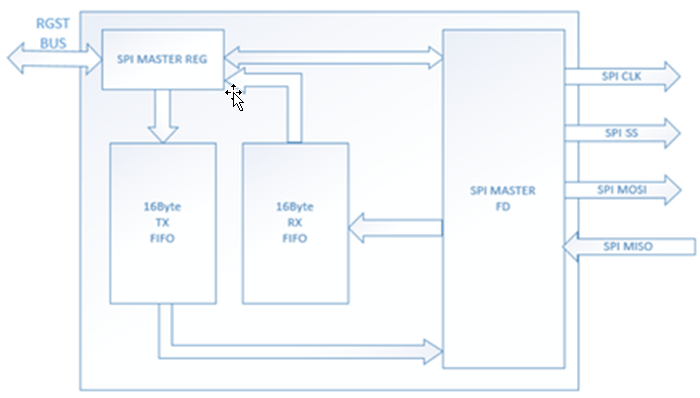
Figure 30-1 SPI Master Full Duplex Function Block
- SPI MISO: Master In/Slave Out data. In the general case, this pin is used to transmit data in slave mode and receive data in the master mode.
- SPI MOSI: Master Out/Slave In data. In the general case, this pin is used to transmit data in master mode and receive data in the slave mode.
- SPI CLK: Serial clock output pin for SPI master and input pin for SPI slave.
- SPI SS: Chip select pin. Controlled by master. The slave will only react to the master's operation command if the /SS signal is low.
- SPI MASTER FD: SPI master full duplex interface.
- RXFIFO: SPI_RXFIFO supports 16-byte received data FIFO. Users can read data from RXFIFO through accessing Group91.9~12 (rx_data3_2_1_0~ rx_data15_14_13_12) registers and check FIFO status through read Group91.14 (spi_status) register bit6~2.
- TXFIFO: SPI_TXFIFO supports 16-byte is used to store the data written by user through Group91.1~4 (tx_data3_2_1_0~ tx_data15_14_13_12) registers and check FIFO status through read Group91.14 (spi_status) register bit6~2.
- SPI MASTER REG: The SPI MASTER control registers bus.
SPI with DMA function blocks are shown in Figure 30-2, Figure 30-3 & Figure 30-4.
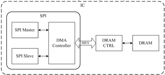
Figure 30-2 SPI DMA Function Block
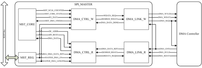
Figure 30-3 SPI Master DMA Function Block
- MST_CORE: Receive or transmit data from or to SPI_SLAVE
- DMA_CTRL_W: Receive DATA from MST_CORE and produce WDATA_REQ with transmit 4-byte data to DMA_LINK_W
- DMA_CTRL_R: Transmit DATA to MST_CORE and produce RDATA_REQ with receive 4-byte data from DMA_LINK_R
- DMA_LINK_R/W: Communicate with DMA_CTRL via proprietary System Bus (SBUS) protocol
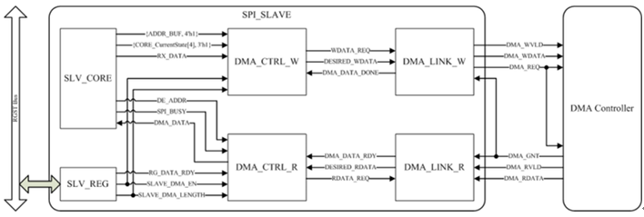
Figure 30-4 SPI Slave DMA Function Block
- SLV_CORE: Receive or transmit from or to SPI_MASTER
- DMA_CTRL_W/R, DMA_LINK_W/R: Function same as above description
- ADDR_BUF: Indicate which RX_DATA is being transmitted through SPI protocol
- CORE_CurrentState[4]: DMA state or not
30.3 SPI Timing Chart
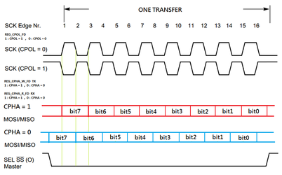
Figure 30-5 SPI Timing Chart
According slave device work timing, the SP7021 SPI master have 4 kinds work mode. User can select SCK polarity and latch data edge to get expected work mode. The register Group91.17 (spi_ctrl_clk_sel) bit3 can be select SCK polarity, "CPOL=0" is SCK stay in low level when stop work, "CPOL=1" is stay in high level. The register Group91.17 (spi_ctrl_clk_sel) bit6 can be select latch data edge during write, "CPHA=0" is latch data in SCK rising edge, "CPHA=1" is latch data in SCK falling edge. The register Group91.17 (spi_ctrl_clk_sel) bit5 can be select latch data edge during read.
30.4 Baud Rate Generation
The SPI output clock frequency can be configured by below formula. SYSCLK/(2(CLK_SEL+1))*CLK_SEL can be selected in register Group91.17 (spi_ctrl_clk_sel) bit29~16.If system clock is 304MHz, the CLK_SEL with the data transfer rate excludes 12-bit address relationship shows as below.
CLK_SEL | SYS_CLK Freq(MHz, 1/T) | SPI_SCLK Freq(MHz, 1/T) | Data Transfer(Without 8bit Address)(MBps) |
0 | 304M | 152M | 152/8=19MBps |
1 | 304M | 76M | 76/8=9.5MBps |
3 | 304M | 38M | 38/8=4.75MBps |
30.5 Addition Delay In Read Operation
There has an addition delay R_DLY can be set in read action. The range is 0~1.5*SPI_CLK_CYCLE. R_DLY can be set in bit[31:30] of Group91.17 spi_ctrl_clt_sel register.
30.6 Address Bit Number
The transfer address bit number can be set as 8/12/16/20bits by ADDR_BIT_NUM which is bit[8:7] of group19.17 spi_ctrl_clt_sel register.
30.7 Slave Enable Polarity
The slave enable pin polarity can be selected by EN_POLARITY. Default set 0 as low active. The EN_POLARITY locate in bit4 of Group91.17 spi_ctrl_clt_sel register.
30.8 RW Position
Chip default set 0 to RW_POSITION, it means Addr[0] is R/W bit, otherwise Addr[7] is R/W bit. The RW_POSITION locate in bit2 of Group91.17 spi_ctrl_clt_sel register.
30.9 LSB Select
Chip default set 0 to LSB_SELECT, it means that data begin at bit0, otherwise at bit7. The LSB_SELECT locate in bit1 of Group91.17 spi_ctrl_clt_sel register.
30.10 SPI Start
SPI master begin write or read action when SPI_START set to 1. It will return to 0 automatically when SPI transmission finish. The SPI_START locate in bit0 of Group91.17 spi_ctrl_clt_sel register.
30.11 Communication between one master and one slave
The SPI support full-duplex communication. In this configuration, the shift registers of master and slave are linked using two unidirectional lines between the MOSI and the MISO pins. During SPI communication, data is shifted synchronously on the SCK clock edges provided by the master. The master transmits the data to be sent to the slave via the MOSI line and receives data from the slave via the MISO line. When the data frame transfer is complete the information between the master and slave is exchanged. Figure 30-6 shows one master and one slave device connected status.
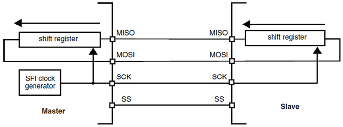
Figure 30-6 One master and one slave communication
30.12 Multi-slave communication
In a configuration with two or more independent slaves, the master uses GPIO pins to manage the chip select lines for each slave (refer to Figure 30-7). The master must select one of the slaves individually by pulling low the GPIO connected to the slave SS input. When this is done, a standard master and dedicated slave communication is established.
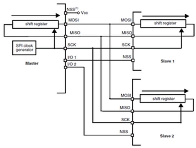
Figure 30-7 Master and two independent slaves
30.13 SPI Operation Mode
30.13.1 SPI-MASTER Write and Read Trigger Flow
- Setup transfer setting (transfer frequency, data byte……………)
- Set data count and transfer data
- Clear SPI status and set interrupt mask
- Set write mode or read mode
- Enable interrupt
- Start transfer
- Wait timer-out or transfer finish
- Reset SPI-MASTER
30.13.2 SPI DMA Read Mode Flow
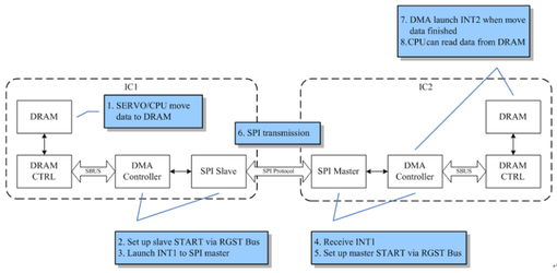
Figure 30-8 SPI DMA Read Mode Flow
- CPU moves data to DRAM in IC1
- Set up slave START via RGST bus
- Issue interrupt to master
- Receive interrupt from slave
- Set up master START via RGST bus
- SPI transmission
- When finished moving data to DRAM, DMA controller issues interrupt to CPU in IC2
- CPU read data from DRAM
30.13.3 SPI DMA Write Mode Flow
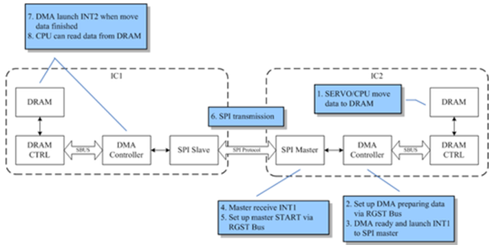
Figure 30-9 SPI DMA Write Mode Flow
- CPU moves data to DRAM in IC2
- Set up master DMA preparing data via RGST bus
- DMA data ready and issue interrupt to master
- Master receives interrupt from DMA
- Set up master START via RGST bus
- SPI transmission
- When finished moving data to DRAM, DMA controller issues interrupt to CPU in IC1
- CPU read data from DRAM
30.14 SPI Interrupts
TX and RX FIFO have full and empty interrupt that can be used in burst mode for full duplex master. When tx fifo empty and rx fifo full interrupt received and transfer have not completed, IRQ handler should move data to or fetch data from tx/rx fifo to continue transfer until it complete.Finish int means SPI Transmission done for full duplex master. IRQ handler can handle the data transferred and start a new transmission for full duplex master.SPI_MASTER_RISC_INT (Group91.19 bit7) is generated from SPI_MST_INT_I and MST_DMA_INT. Set INT_EDGE (Group91.19 bit5) register or INT_BYPASS (Group91.19 bit3) register to configure interrupt. SPI_MST_INT_I Interrupt is issued when incoming SPI interrupt to SPI MASTER. MST_DMA_INT interrupt is issued when DMA data is ready (MST_DMA_DATA_RDY). IRQ handler will immediately set up master START via RGST bus and start SPI transmission.
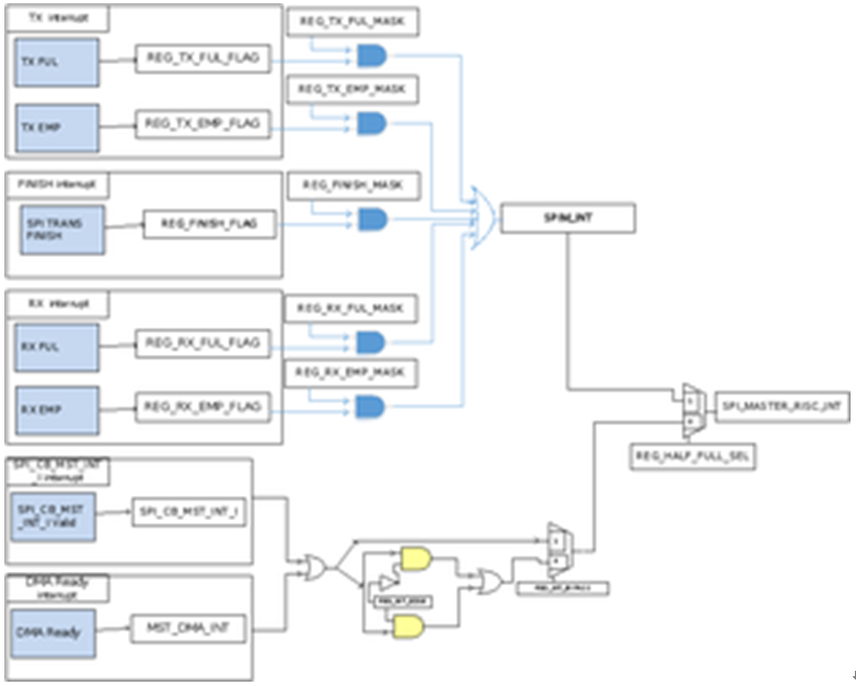
Figure 30-10 SPI MASTER RISC INT
SPI_ SLAVE_INT (Group92.17 bit9) interrupt is issued when SPI slave is not busy. IRQ handler can get data transferred and start a new transmission.

Figure 30-11 SPI SLAVE INT
SPI_DMA_W_INT (Group91.20 bit8) interrupt is issued when SPI DMA data transfer is done. IRQ handler can read data from DRAM.

Figure 30-12 SPI DMA W INT
30.15 Registers Map
30.15.1 Register Memory Map
SPI Register Memory Map
Group Base Address | Data Width | Group No. | Module |
0x9C002D80 | 32 | 91 | SPI_MASTER_0 |
0x9C002E00 | 32 | 92 | SPI_SLAVE_0 |
0x9C00F480 | 32 | 489 | SPI_MASTER_1 |
0x9C00F500 | 32 | 490 | SPI_SLAVE_1 |
0x9C00F600 | 32 | 492 | SPI_MASTER_2 |
0x9C00F680 | 32 | 493 | SPI_SLAVE_2 |
0x9C00F780 | 32 | 495 | SPI_MASTER_3 |
0x9C00F800 | 32 | 496 | SPI_SLAVE_3 |
Table 30-1 SPI Register Memory Map
All SPIs' registers have the same offset (address - base address) in corresponding SPI register group. Only SPI0 Master and Slave registers are described in following register description, for other SPIs (SPI1, 2, 3) please refer to SPI0 description for more detail.
30.15.2 Registers Description
SPI Register Description
RGST Table Group 91 SPI MASTER 0
91.0 Transmit register1 (tx data addr)
Address: 0x9C002D80
Reset: 0x0000 0000
Field Name | Bit | Access | Description |
Reserve | 31:20 | RO | Reserved |
ADDR | 19:0 | RW | Address for SPI master to transmit in write/ read action |
91.1 Transmit register2 (tx data3 2 1 0)
Address: 0x9C002D84
Reset: 0x0000 0000
Field Name | Bit | Access | Description |
TX DATA 3 | 31:24 | RW | Byte3 data for SPI master to transmit in write action |
TX DATA 2 | 23:16 | RW | Byte2 data for SPI master to transmit in write action |
TX DATA 1 | 15:8 | RW | Byte1 data for SPI master to transmit in write action |
TX DATA 0 | 7:0 | RW | Byte0 data for SPI master to transmit in write action |
91.2 Transmit register3 (tx data7 6 5 4)
Address: 0x9C002D88
Reset: 0x0000 0000
Field Name | Bit | Access | Description |
TX DATA 5 | 15:8 | RW | Byte5 data for SPI master to transmit in write action |
TX DATA 4 | 7:0 | RW | Byte4 data for SPI master to transmit in write action |
91.3 Transmit register4 (tx data11 10 9 8)
Address: 0x9C002D8C
Reset: 0x0000 0000
Field Name | Bit | Access | Description |
TX DATA11 | 31:24 | RW | Byte11 data for SPI master to transmit in write action |
TX DATA 10 | 23:16 | RW | Byte10 data for SPI master to transmit in write action |
TX DATA 9 | 15:8 | RW | Byte9 data for SPI master to transmit in write action |
TX DATA 8 | 7:0 | RW | Byte8 data for SPI master to transmit in write action |
91.4 Transmit register5 (tx data15 14 13 12)
Address: 0x9C002D90
Reset: 0x0000 0000
Field Name | Bit | Access | Description |
TX DATA15 | 31:24 | RW | Byte15 data for SPI master to transmit in write action |
TX DATA14 | 23:16 | RW | Byte14 data for SPI master to transmit in write action |
TX DATA13 | 15:8 | RW | Byte13 data for SPI master to transmit in write action |
TX DATA12 | 7:0 | RW | Byte12 data for SPI master to transmit in write action |
91.9 Receive register1 (rx data3 2 1 0)
Address: 0x9C002DA4
Reset: 0x0000 0000
Field Name | Bit | Access | Description |
RX DATA 3 | 31:24 | RO | Byte3 data that SPI master receive in read action |
RX DATA 2 | 23:16 | RO | Byte2 data that SPI master receive in read action |
RX DATA 1 | 15:8 | RO | Byte1 data that SPI master receive in read action |
RX DATA 0 | 7:0 | RO | Byte0 data that SPI master receive in read action |
91.10 Receive register2 (rx data7 6 5 4)
Address: 0x9C002DA8
Reset: 0x0000 0000
Field Name | Bit | Access | Description |
RX DATA 7 | 31:24 | RO | Byte7 data that SPI master receive in read action |
RX DATA 6 | 23:16 | RO | Byte6 data that SPI master receive in read action |
RX DATA 5 | 15:8 | RO | Byte5 data that SPI master receive in read action |
RX DATA 4 | 7:0 | RO | Byte4 data that SPI master receive in read action |
91.11 Receive register3 (rx data11 10 9 8)
Address:0x9C002DAC
Reset: 0x0000 0000
Field Name | Bit | Access | Description |
RX DATA 11 | 31:24 | RO | Byte11 data that SPI master receive in read action |
RX DATA 10 | 23:16 | RO | Byte10 data that SPI master receive in read action |
RX DATA 9 | 15:8 | RO | Byte9 data that SPI master receive in read action |
RX DATA 8 | 7:0 | RO | Byte8 data that SPI master receive in read action |
91.12 Receive register4 (rx data15 14 13 12)
Address: 0x9C002DB0
Reset: 0x0000 0000
Field Name | Bit | Access | Description |
RX DATA 15 | 31:24 | RO | Byte15 data that SPI master receive in read action |
RX DATA 14 | 23:16 | RO | Byte14 data that SPI master receive in read action |
RX DATA 13 | 15:8 | RO | Byte13 data that SPI master receive in read action |
RX DATA 12 | 7:0 | RO | Byte12 data that SPI master receive in read action |
91.13 rx/tx fifo data out/in register for full duplex (fifo_data)
Address: 0x9C002DB4
Reset: 0x0000 0000
Field Name | Bit | Access | Description |
fifo_data | 31:0 | RO | rx/tx fifo data out/in register for full duplex |
91.14 spi master status for full duplex (spi_status)
Address: 0x9C002DB8
Reset: 0x0000 0000
Field Name | Bit | Access | Description |
REG_TOTAL_LENGTH_FD | 31:24 | RW | Total length for full duplex |
REG_TX_LENGTH_FD | 23:16 | RW | TX length for full duplex max 255 byte,less than total length |
REG_RX_CNT | 15:12 | RO | RX FIFO CNT for full duplex data byte in rx fifo, |
REG_TX_CNT | 11:8 | RO | TX FIFO CNT for full duplex data byte in tx fifo, |
REG_SPI_BUSY_FD | 7 | RO | SPI_BUSY for full duplex 0: busy |
REG_FINISH_FLAG | 6 | WO | FINISH_FLAG for full duplex |
REG_RX_FUL_FLAG | 5 | RO | RX_FIFO_FUL_FLAG for full duplex |
REG_RX_EMP_FLAG | 4 | RO | RX_FIFO_EMP_FLAG for full duplex |
REG_TX_FUL_FLAG | 3 | RO | TX_FIFO_FUL_FLAG for full duplex |
REG_TX_EMP_FLAG | 2 | RO | TX_FIFO_EMP_FLAG for full duplex |
REG_MASTER_SW_RST | 1 | RO | SW RST for full duplex |
REG_SPI_START_FD | 0 | RO | SPI START for full duplex |
91.15 spi master config for full duplex (spi_config)
Address: 0x9C002DBC
Reset: 0x0000 0000
Field Name | Bit | Access | Description |
REG_SPI_CLK_CNT_FD | 31:16 | RW | Ratio between SPI clk and sysclk |
REG_FINISH_MASK | 15 | RW | FINISH_MASK for full duplex |
REG_RX_FUL_MASK | 14 | RW | RX_FIFO_FUL_MASK for full duplex |
REG_RX_EMP_MASK | 13 | RW | RX_FIFO_EMP_MASK for full duplex |
REG_TX_FUL_MASK | 12 | RW | TX_FIFO_FUL_MASK for full duplex |
REG_TX_EMP_MASK | 11 | RW | TX_FIFO_EMP_MASK for full duplex |
REG_WRITE_BYTE | 10:9 | RW | WRITE_BYTE for full duplex |
REG_READ_BYTE | 8:7 | RW | READ_BYTE for full duplex |
REG_HALF_FULL_SEL | 6 | RO | HALF_FULL_SEL for full duplex 0: half duplex mode |
REG_EN_POR_FD | 5 | RW | EN POLARITY for full duplex 0: cs low active |
REG_LSB_SEL_FD | 4 | RW | LSB SELECT for full duplex 0: msb |
REG_DELAY_FD | 3 | RW | DEALY ENABLE IN RX for full duplex |
REG_CPHA_W_FD | 2 | RW | CPHA_W TX for full duplex 0: first edge launch |
REG_CPHA_R_FD | 1 | RW | CPHA_R RX for full duplex 0: first edge capture |
REG_CPOL_FD | 0 | RW | CPOL for full duplex 0: clk low when idle |
91.17 SPI master control and clock select register (spi ctrl clk sel)
Address: 0x9C002DC4
Reset: 0x0000 0000
Field Name | Bit | Access | Description |
R DLY | 31:30 | RW | Additional delay in read action 0x0: No delay(default) |
SPI CLOCK SEL | 29:16 | RW | Ratio between SPI clk and sysclk1/(2*(CLK SEL+1)) |
Reserve | 15:9 | RW | Reserved |
ADDR BIT NUM | 8:7 | RW | Transfer address bit number 0x0: 12-bit |
WRITE SAMPLING EDGE | 6 | RW | SPI TX edge 0: Rising edge of SPI clk(default) |
READ SAMPLING EDGE | 5 | RW | SPI RX edge 0: Rising edge of SPI clk(default) |
EN POLARITY | 4 | RW | SPI CS polarity 0: Low active(default) |
READ POLARITY | 3 | RW | Read/Write bit polarity 0: High read(default) |
RW POSITION | 2 | RW | Read/Write bit position 0: Addr[0] is R/W bit(default) |
SB SELECT | 1 | RW | LSB enable in SPI transmission 0: Begin at bit0(default) |
SPISTART | 1 | WO | SPI transmission start 1: SPI master begin write/ read action |
91.18 SPI transmission byte No. register (byte no)
Address: 0x9C002DC8
Reset: 0x0000 0000
Field Name | Bit | Access | Description |
Reserve | 31:5 | RO | Reserved |
BYTE NO | 4:0 | RW | No. of bytes in SPI transmission Support from 1-byte to 16-byte |
91.19 SPI master interrupt control register (spi int busy)
Address: 0x9C002DCC
Reset: 0x0000 0020
Field Name | Bit | Access | Description |
Reserve | 31:10 | RO | RESERVED |
PI BUSY FLAG | 9 | RO | Indicator of BUSY signal from TI2046 chip |
PI BUSY EN | 8 | RO | Support TI2046 BUSY signal Return data is valid when busy signal is low after SPI MASTER issues command. |
MASTER INT STATUS | 7 | RO | Master interrupt to RISC |
MASTER INT CLR | 6 | RW | Master INT clear 1: Clear SPI master interrupt |
REG INT EDGE | 5 | RW | Define incoming SPI interrupt trigger polarity 0: low level or falling edge interrupt |
REG INT TYPE | 4 | RW | Define incoming SPI interrupt trigger type 0: level interrupt(default) |
REG INT BYPASS | 3 | RW | SPI master INT bypass 0: SPI master INT comes from SPI master module(default) |
REG INT TIMEOUT | 2 | RW | SPI master INT timeout function SPI master module will launch SPI master INT again when CPU has served INT but the incoming SPI interrupt is still in active state. |
RW PHASE | 1 | RO | Indicator of SPI write/ read action 0: read(default) |
REG SPI BUSY | 0 | RO | Indicator of SPI master operation status 0: SPI master is not in operation(default) |
91.20 SPI master DMA control register (master dma ctrl)
Address: 0x9C002DD0
Reset: 0x0000 0000
Field Name | Bit | Access | Description |
Reserve | 31:9 | RO | RESERVED |
DMA W INT STATUS | 8 | RO | DMA Write interrupt status Whether DMA transmission is finished or not. |
DMA W INT CLR | 7 | RW | DMA Write interrupt clear 1: Clear DMA write interrupt |
DMA RW SEL | 6 | RW | DMA read/write select 0: DMA write to DRAM(default) |
DMA BANK | 5 | RW | DRAM bank select 0x0: Bank A(default) |
MASTER DMA BP WBE | 4 | RWRW | SBUS write-byte enable select 0: With write-byte-enable(default) |
MASTER DMA BURST | 3:2 | SBUS command select 0x0: 4 bytes command(default) | |
MASTER MASTER SW RST | 1 | RW | SPI master software reset 0: Disable(default) |
MASTER DMA EN | 0 | RW | DMA function select 0: Disable(default) |
91.21 SPI master DMA length register (master dma length)
Address: 0x9C002DD4
Reset: 0x0000 0000
Field Name | Bit | Access | Description |
Reserve | 31:18 | RO | RESERVED |
MASTER DMA LENGTH | 17:0 | RW | Total data length in DMA transmission (unit:byte) |
91.22 SPI master DMA address register (master dma addr)
Address: 0x9C002DD8
Reset: 0x0000 0000
Field Name | Bit | Access | Description |
MASTER DMA ADDR | 31:0 | RW | Start address in DRAM to store data (unit:byte) |
91.24 SPI master DMA address status register (dma addr status)
Address: 0x9C002DE0
Reset: 0x0000 0000
Field Name | Bit | Access | Description |
DMA ADDR STATUS | 31:0 | RO | DMA address status Return address which DMA access |
91.26 Uart DMA control register (uart dma ctrl)
Address:0x9C002DE8
Reset: 0x0000 0000
Field Name | Bit | Access | Description |
Reserve | 31:3 | RO | RESERVED |
UART SW RST | 2 | RW | Software reset when SPI in UART DMA mode |
UART DMA START | 1 | W1C | DMA transmission start signal from UART 1: DMA transmission start ; it will return to 0 automatically. |
UART DMA EN | 0 | RW | DMA function select from UART 0: Disable(default) |
91.28 Reserved (reserved)
Address: 0x9C002DF0
Reset: 0x0000 0000
Field Name | Bit | Access | Description |
Reserve | 31:0 | RO | Reserved for Internal usage purpose |
91.29 Reserved (Reserved)
Address: 0x9C002DF4
Reset: 0x0000 0000
Field Name | Bit | Access | Description |
Reserve | 31:0 | RO | Reserved for Internal usage purpose |
91.30 SPI extra cycle control register (spi extra cycle ctrl)
Address: 0x9C002DF8
Reset: 0x0000 0000
Field Name | Bit | Access | Description |
Reserve | 31:4 | RO | RESERVED |
SPI EXTRA CYCLE | 3:2 | RW | Choose the number of SPI extra cycle. These settings take effect ONLY when SPI EXTRA CYCLE EN=1'b1 0x0: Add extra 1 SPI cycle(default) |
SPI EN CUT | 1 | RW | SPI EN output interval select This setting takes effect ONLY when SPI EXTRA CYCLE EN=1'b1 0: SPI EN output interval will be SPI read plus SPI extra cycle.(default) |
SPI EXTRA CYCLE EN | 0 | RW | Enable SPI extra cycle to fix path delay in SPI read process 0: Disable(default) |
91.31DMA data ready register (dma data ready)
Address: 0x9C002DFC
Reset: 0x0000 0000
Field Name | Bit | Access | Description |
Reserve | 31:1 | RO | RESERVED |
MST DMA DATA RDY | 0 | RO | DMA Read data prefetch ready |
RGST Table Group 92 SPI SLAVE0
92.0 SPI slave transmit data register1 (tx data2 1 0)
Address: 0x9C002E00
Reset: 0x0000 0000
Field Name | Bit | Access | Description |
RESERVED | 31:24 | RO | RESERVED |
TX DATA 2 | 23:16 | RW | Byte2 data for SPI slave to transmit in read action |
TX DATA 1 | 15:8 | RW | Byte1 data for SPI slave to transmit in read action |
TX DATA 0 | 7:0 | RW | Byte0 data for SPI slave to transmit in read action |
92.1SPI slave transmit data register2 (tx data6 5 4 3)
Address: 0x9C002E04
Reset: 0x0000 0000
Field Name | Bit | Access | Description |
TX DATA 6 | 31:24 | RW | Byte6 data for SPI slave to transmit in read action |
TX DATA 5 | 23:16 | RW | Byte5 data for SPI slave to transmit in read action |
TX DATA 4 | 15:8 | RW | Byte4 data for SPI slave to transmit in read action |
TX DATA 3 | 7:0 | RW | Byte3 data for SPI slave to transmit in read action |
92.2 SPI slave transmit data register3 (tx data10 9 8 7)
Address: 0x9C002E08
Reset: 0x0000 0000
Field Name | Bit | Access | Description |
TX DATA 10 | 31:24 | RW | Byte10 data for SPI slave to transmit in read action |
TX DATA 9 | 23:16 | RW | Byte9 data for SPI slave to transmit in read action |
TX DATA 8 | 15:8 | RW | Byte8 data for SPI slave to transmit in read action |
TX DATA 7 | 7:0 | RW | Byte7 data for SPI slave to transmit in read action |
92.3 SPI slave transmit data register4 (tx data14 13 12 11)
Address:0x9C002E0C
Reset: 0x0000 0000
Field Name | Bit | Access | Description |
TX DATA 14 | 31:24 | RW | Byte14 data for SPI slave to transmit in read action |
TX DATA 13 | 23:16 | RW | Byte13 data for SPI slave to transmit in read action |
TX DATA 12 | 15:8 | RW | Byte12 data for SPI slave to transmit in read action |
TX DATA 11 | 7:0 | RW | Byte11 data for SPI slave to transmit in read action |
92.4 SPI slave transmit data register5 (tx data15)
Address: 0x9C002E10
Reset: 0x0000 0000
Field Name | Bit | Access | Description |
RESERVED | 31:8 | RO | RESERVED |
TX DATA 15 | 7:0 | RW | Byte15 data for SPI slave to transmit in read action |
92.9 SPI slave receive data register1 (rx data3 2 1 0)
Address: 0x9C002E24
Reset: 0x0000 0000
Field Name | Bit | Access | Description |
RX DATA 3 | 31:24 | RO | Byte3 data that SPI slave receive in write action |
RX DATA 2 | 23:16 | RO | Byte2 data that SPI slave receive in write action |
RX DATA 1 | 15:8 | RO | Byte1 data that SPI slave receive in write action |
RX DATA 0 | 7:0 | RO | Byte0 data that SPI slave receive in write action |
92.10 SPI slave receive data register2 (rx data7 6 5 4)
Address: 0x9C002E28
Reset: 0x0000 0000
Field Name | Bit | Access | Description |
RX DATA 7 | 31:24 | RO | Byte7 data that SPI slave receive in write action |
RX DATA 6 | 23:16 | RO | Byte6 data that SPI slave receive in write action |
RX DATA 5 | 15:8 | RO | Byte5 data that SPI slave receive in write action |
RX DATA 4 | 7:0 | RO | Byte4 data that SPI slave receive in write action |
92.11 SPI slave receive data register3 (rx data11 10 9 8)
Address: 0x9C002E2C
Reset: 0x0000 0000
Field Name | Bit | Access | Description |
RX DATA 11 | 31:24 | RO | Byte11 data that SPI slave receive in write action |
RX DATA 10 | 23:16 | RO | Byte10 data that SPI slave receive in write action |
RX DATA 9 | 15:8 | RO | Byte9 data that SPI slave receive in write action |
RX DATA 8 | 7:0 | RO | Byte8 data that SPI slave receive in write action |
92.12 SPI slave receive data register7 (rx data15 14 13 12)
Address: 0x9C002E30
Reset: 0x0000 0000
Field Name | Bit | Access | Description |
RX DATA 15 | 31:24 | RO | Byte15 data that SPI slave receive in write action |
RX DATA 14 | 23:16 | RO | Byte14 data that SPI slave receive in write action |
RX DATA 13 | 15:8 | RO | Byte13 data that SPI slave receive in write action |
RX DATA 12 | 7:0 | RO | Byte12 data that SPI slave receive in write action |
92.17 SPI slave interrupt register (risc int data rdy)
Address: 0x9C002E44
Reset: 0x0000 0000
Field Name | Bit | Access | Description |
RESERVED | 31:10 | RO | RESERVED |
SPI SLAVE INT | 9 | RO | SPI Slave Interrupt Register SPI slave will launch INT to CPU when SPI transmission is finished no matter write or read action. |
SLAVE INT CLR | 8 | RW | SPI slave INT clear 1: Clear SPI slave interruptit will return to 0 automatically when interrupt is low. |
RESERVED | 7:1 | RO | RESERVED |
SLAVE DATA RDY | 0 | RW | SPI slave data ready signal 1: SPI slave data is ready and launch INT to SPI master. It will return to 0 automatically. |
92.18 SPI slave DMA control register (slave dma ctrl)
Address: 0x9C002E48
Reset: 0x0000 0000
Field Name | Bit | Access | Description |
RESERVED | 31:7 | RO | RESERVED |
SLAVE DMA RW SEL | 6 | RW | SLAVE DMA read/write select 0: DMA write to DRAM(default) |
SLAVE DMA BANK | 5 | RW | DRAM bank select 0: Bank A(default) |
SLAVE DMA BP WBE | 4 | RW | SBUS write-byte enable select 0: With write-byte-enable(default) |
SLAVE DMA BURST | 3:2 | RW | SBUS command select 0x0: 4 bytes command(default) |
SLAVE SLAVE SW RST | 1 | RW | SPI slave software reset 0: Disable(default) |
SLAVE DMA EN | 0 | RW | DMA function select 0: Disable(default) |
92.19 SPI slave DMA length register (slave dma length)
Address: 0x9C002E4C
Reset: 0x0000 0000
Field Name | Bit | Access | Description |
RESERVED | 31:18 | RO | RESERVED |
SLAVE DMA LENGTH | 17:0 | RW | Total data length in DMA transmission (unit:byte) |
92.20 SPI slave DMA address register (slave dma addr)
Address:0x9C002E50
Reset: 0x0000 0000
Field Name | Bit | Access | Description |
SLAVE DMA ADDR | 31:0 | RW | Slave Mode DMA Start Address |
92.23 SPI slave index signal register (addr spi busy)
Address: 0x9C002E5C
Reset: 0x0000 0000
Field Name | Bit | Access | Description |
RESERVED | 31:15 | RO | RESERVED |
SLAVE ADDR INFO | 14:8 | RO | Address info inside SPI slave module |
RESERVED | 7:2 | RO | RESERVED |
SLAVE RWPHASE | 1 | RO | Indicator of SPI write/read action 0: read (default) |
SLAVE BUSY | 0 | RO | Indicator of SPI slave operation status 0: SPI slave is not in operation (default) |
92.24 Reserved (Reserved)
Address: 0x9C002E60
Reset: 0x0000 0000
Field Name | Bit | Access | Description |
RESERVED | 31:0 | RO | RESERVED |
RGST Table Group 489 SPI MASTER1 (Base Address: 0x9C00F480, Please refer to SPI MASTER0 register offset and description for more detail)
RGST Table Group 490 SPI SLAVE1 (Base Address: 0x9C00F500, Please refer to SPI SLAVE0 register offset and description for more detail)
RGST Table Group 492 SPI MASTER2 (Base Address: 0x9C00F600, Please refer to SPI MASTER0 register offset and description for more detail)
RGST Table Group 493 SPI SLAVE2 (Base Address: 0x9C00F680, Please refer to SPI SLAVE0 register offset and description for more detail)
RGST Table Group 495 SPI MASTER3 (Base Address: 0x9C00F780, Please refer to SPI MASTER0 register offset and description for more detail)
RGST Table Group 496 SPI SLAVE3 (Base Address: 0x9C00F800, Please refer to SPI SLAVE0 register offset and description for more detail)