...
Group101.25~31 (abbreviation as G101.25~31) registers are used for set GPIO_FIRST (for pad control, “1” means GPIO, “0” means Multiplex function ) state. Each bit map to one pin. For example, G101.25[0] control GPIO_P0_00 pin’s GPIO_FIRST state.
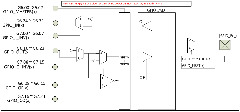
Figure 4. Pin Assignment
...
GPIO Block Diagram
5.3.1. Set General Purpose I/O Pin Method
First step is setting GPIO_MASTER bit to “1”, it means source select as GPIO or IOP(8051).
...
GPIO_P0 port default set as GPIO function.
...
5.3.2. GPIO control method
For example, set GPIO_P0_00 as output without open drain, please set as below:
Action | Step |
Set GPIO_P0_00 as output without open drain | Step1 : G7.16=0x00010000h , OD = 0 (set bit0 as 0) Step2 : G6.16=0x00010001h , OUT = 1 (set bit0 as 1) Step3 : G6.08=0x00010001h , OE = 1 (set bit0 as 1) |
...
For example, set GPIO_P1_00 as output with open drain, please set as below:
Action | Step |
Set GPIO_P1_00 as output with open drain | Step1 : G7.16=0x01000100h , OD =1 (set bit8 as 1) Step2 : G6.16=0x01000100h , OUT = 1 (set bit8 as 1) Step3 : G6.08 OE = X (don’t care) |
...
5.4. How to program Multiplex Peripheral Pins
All Multiplex Peripheral Pins support means that you can set all Multiplex Peripheral Pin output through GPIO1 ~ GPIO8 ports. Multiplex Peripheral Pins include: ETH_SW, SDIO, PWM, Input Capture, SPI MASTER, SPI SLAVE, I2C MASTER, UART(1~4), TIMER, GPIO INT. Multiplex Peripheral Pin hardware block show as below figure.
...
Please notice that user should prevent set several signals in the same pin, one signal only can be assign to one pin.
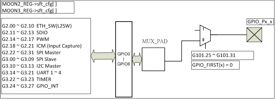
Figure 5. Multiplex Peripheral Pin AssignmentBlock Diagram
...
5.4.1. Set Multiplex Peripheral Pin Method
Just need to set GPIO_FIRST bit to “0” , GPIO_MASTER bit set “X” means don’t care in this case. Regarding registers map, please check 6.3.1 .
For example, set GPIO_P1_00 pin to general purpose I/O function, please set registers values as below:
Multiplex Peripheral Pin | |
G6.0 bit8: GPIO_MASTER | X |
G101.25 bit8: GPIO_FIRST | 0 |
GPIO_P1~8 ports default set as Multiplex Peripheral Pin.
...
5.4.2. Set Multiplex Peripheral Pin - ETHERNET_SWITCH pins
There have 2 ETH_SW ports supported in this chip , Each ETH_SW module have 11pins, user can select any signals output in any pins of GPIO_P1~8. The registers G2.0~G2.10 can be used for select ETH_SW signals and pins.
...
ETH_SW0 function | Value | GPIO pins map |
G2.0[7~0] L2SW_CLK_OUT | 43 | GPIO_P6_02 |
G2.0[15~8] L2SW_MAC_SMI_MDC | 37 | GPIO_P5_04 |
G2.1[7~0] L2SW_LED_FLASH0 | 47 | GPIO_P6_06 |
G2.2[7~0] L2SW_LED_ON0 | 38 | GPIO_P5_05 |
G2.3[7~0] L2SW_MAC_SMI_MDIO | 36 | GPIO_P5_03 |
G2.3[15~8] L2SW_P0_MAC_RMII_TXEN | 46 | GPIO_P6_05 |
G2.4[7~0] L2SW_P0_MAC_RMII_TXD0 | 44 | GPIO_P6_03 |
G2.4[15~8] L2SW_P0_MAC_RMII_TXD1 | 45 | GPIO_P6_04 |
G2.5[7~0] L2SW_P0_MAC_RMII_CRSDV | 40 | GPIO_P5_07 |
G2.5[15~8] L2SW_P0_MAC_RMII_RXD0 | 41 | GPIO_P6_00 |
G2.6[7~0] L2SW_P0_MAC_RMII_RXD1 | 42 | GPIO_P6_01 |
G2.6[15~8] L2SW_P0_MAC_RMII_RXER | 39 | GPIO_P5_06 |
...
5.4.3. Set Multiplex Peripheral Pin - SDIO pins
Method same as 65.4.2.
For example, set SDIO port to GPIO_P8_01~06 pins.
SDIO function | Value | GPIO pins map |
G2.11[7~0] SDIO_CLK | 60 | GPIO_P8_03 |
G2.11[15~8] SDIO_CMD | 61 | GPIO_P8_04 |
G2.12[7~0] SDIO_D0 | 59 | GPIO_P8_02 |
G2.12[15~8] SDIO_D1 | 58 | GPIO_P8_01 |
G2.13[7~0] SDIO_D2 | 63 | GPIO_P8_06 |
G2.13[15~8] SDIO_D3 | 62 | GPIO_P8_05 |
...
5.4.4. Set Multiplex Peripheral Pin - PWM pins
Method same as 65.4.2.
For example, set PWM0~3 to GPIO_P3_04~07 pins.
PWM function | Value | GPIO pins map |
G2.14[7~0] PWM0 | 21 | GPIO_P3_04 |
G2.14[15~8] PWM1 | 22 | GPIO_P3_05 |
G2.15[7~0] PWM2 | 23 | GPIO_P3_06 |
G2.15[15~8] PWM3 | 24 | GPIO_P3_07 |
...
5.4.5. Set Multiplex Peripheral Pin - Input Capture pins
Method same as 65.4.2.
For example, set ICM0~1 to GPIO_P4_00~03 pins.
ICM function | Value | GPIO pins map |
G2.18[7~0] ICM0_D | 25 | GPIO_P4_00 |
G2.18[15~8] ICM1_D | 27 | GPIO_P4_02 |
G2.20[7~0] ICM0_CLK | 26 | GPIO_P4_01 |
G2.20[15~8] ICM1_CLK | 28 | GPIO_P4_03 |
...
5.4.6. Set Multiplex Peripheral Pin - SPI MASTER pins
Method same as 65.4.2.
For example, set SPIM0 to GPIO_P1_06~07 and GPIO_P2_00~02 pins.
SPI MASTER function | Value | GPIO pins map |
G2.22[7~0] SPIM0_INT | 7 | GPIO_P1_06 |
G2.22[15~8] SPIM0_CLK | 8 | GPIO_P1_07 |
G2.23[7~0] SPIM0_EN | 9 | GPIO_P2_00 |
G2.23[15~8] SPIM0_DO | 10 | GPIO_P2_01 |
G2.24[7~0] SPIM0_DI | 11 | GPIO_P2_02 |
...
5.4.7. Set Multiplex Peripheral Pin - I2C MASTER pins
Method same as 65.4.2.
For example, set I2CM0 to GPIO_P3_00~01 pins.
I2C MASTER function | Value | GPIO pins map |
G3.10[7~0] I2CM0_CK | 17 | GPIO_P3_00 |
G3.10[15~8] I2CM0_DAT | 18 | GPIO_P3_01 |
...
5.4.8. Set Multiplex Peripheral Pin - UART pins
Method same as 65.4.2.
For example, set UART1 to GPIO_P1_00~01 pins.
UART1 function | Value | GPIO pins map |
G3.14[7~0] UA1_TX | 1 | GPIO_P1_00 |
G3.14[15~8] UA1_RX | 2 | GPIO_P1_01 |
...
5.4.9. Set Multiplex Peripheral Pin - TIMER_INT pins
Method same as 65.4.2.
For example, set TIMER0~1_INT to GPIO_P4_04~05 pins.
TIMER_INT function | Value | GPIO pins map |
G3.22[7~0] TIMER0_INT | 29 | GPIO_P4_04 |
G3.22[15~8] TIMER1_INT | 30 | GPIO_P4_05 |
...
5.4.10. Set Multiplex Peripheral Pin - GPIO_INT pins
Method same as 65.4.2.
For example, set GPIO_INT0~1 to GPIO_P5_00~01 pins.
TIMER_INT function | Value | GPIO pins map |
G3.24[7~0] GPIO_INT0 | 33 | GPIO_P5_00 |
G3.24[15~8] GPIO_INT1 | 34 | GPIO_P5_01 |
...
5.5. How to program FBIO function
FBIO function mode can be enabled while G1.1 register bit12 set to 1, GPIO_P0_02 ~ GPIO_P5_02 pins will be set to FBIO function for FPGA usage. But the priority is GPIO function > Multiplex Peripheral Pin > FBIO Function. While use FBIO function, do not set GPIO function and Multiplex Peripheral Pin within GPIO_P0_02 ~ GPIO_P5_02 pins.
...
5.6. How to program LCDIF function
LCDIF function mode can be enabled while G1.4 register bit6 set to 1, GPIO_P1_04 ~ GPIO_P4_07 pins will be set to LCDIF function for LCD display usage.
...
5.7. How to program HDMIDDC function
HDMIDDC function mode can be enabled while G1.1 register bit14 set 1 and bit13 set 0, GPIO_P8_03 ~ GPIO_P8_06 pins will be set to HDMIDDC function for HDMI display data channel communication usage.
HDMIDDC function mode can be enabled while G1.1 register bit14 set 1 and bit13 set 1, GPIO_P7_04 ~ GPIO_P7_07 pins will be set to HDMIDDC function for HDMI display data channel communication usage.
...
5.8. Register Map for Multiplex Pins
Address | Group2 | Byte3 | Byte2 | Byte1 | Byte0 |
|---|---|---|---|---|---|
0x9C00 0100 | G2.0 | X | X | L2SW_MAC_SMI_MDC(0-64) | L2SW_CLK_OUT(0-64) |
0x9C00 0104 | G2.1 | X | X | L2SW_LED_FLASH1(0-64) | L2SW_LED_FLASH0(0-64) |
0x9C00 0108 | G2.2 | X | X | L2SW_LED_ON1(0-64) | L2SW_LED_ON0(0-64) |
0x9C00 010C | G2.3 | X | X | L2SW_P0_MAC_RMII_TXEN(0-64) | L2SW_MAC_SMI_MDIO(0-64) |
0x9C00 0110 | G2.4 | X | X | L2SW_P0_MAC_RMII_TXD1(0-64) | L2SW_P0_MAC_RMII_TXD0(0-64) |
0x9C00 0114 | G2.5 | X | X | L2SW_P0_MAC_RMII_RXD0(0-64) | L2SW_P0_MAC_RMII_CRSDV(0-64) |
0x9C00 0118 | G2.6 | X | X | L2SW_P0_MAC_RMII_RXER(0-64) | L2SW_P0_MAC_RMII_RXD1(0-64) |
0x9C00 011C | G2.7 | X | X | L2SW_P1_MAC_RMII_TXD0(0-64) | L2SW_P1_MAC_RMII_TXEN(0-64) |
0x9C00 0120 | G2.8 | X | X | L2SW_P1_MAC_RMII_CRSDV(0-64) | L2SW_P1_MAC_RMII_TXD1(0-64) |
0x9C00 0124 | G2.9 | X | X | L2SW_P1_MAC_RMII_RXD1(0-64) | L2SW_P1_MAC_RMII_RXD0(0-64) |
0x9C00 0128 | G2.10 | X | X | DAISY_MODE(0-64) | L2SW_P1_MAC_RMII_RXER(0-64) |
0x9C00 012C | G2.11 | X | X | SDIO_CMD(0-64) | SDIO_CLK(0-64) |
0x9C00 0130 | G2.12 | X | X | SDIO_D1(0-64) | SDIO_D0(0-64) |
0x9C00 0134 | G2.13 | X | X | SDIO_D3(0-64) | SDIO_D2(0-64) |
0x9C00 0138 | G2.14 | X | X | PWM1(0-64) | PWM0(0-64) |
0x9C00 013C | G2.15 | X | X | PWM3(0-64) | PWM2(0-64) |
0x9C00 0140 | G2.16 | X | X | PWM5(0-64) | PWM4(0-64) |
0x9C00 0144 | G2.17 | X | X | PWM7(0-64) | PWM6(0-64) |
0x9C00 0148 | G2.18 | X | X | ICM1_D(0-64) | ICM0_D(0-64) |
0x9C00 014C | G2.19 | X | X | ICM3_D(0-64) | ICM2_D(0-64) |
0x9C00 0150 | G2.20 | X | X | ICM1_CLK(0-64) | ICM0_CLK(0-64) |
0x9C00 0154 | G2.21 | X | X | ICM3_CLK(0-64) | ICM2_CLK(0-64) |
0x9C00 0158 | G2.22 | X | X | SPIM0_CLK(0-64) | SPIM0_INT(0-64) |
0x9C00 015C | G2.23 | X | X | SPIM0_DO(0-64) | SPIM0_EN(0-64) |
0x9C00 0160 | G2.24 | X | X | SPIM1_INT(0-64) | SPIM0_DI(0-64) |
0x9C00 0164 | G2.25 | X | X | SPIM1_CEN(0-64) | SPIM1_CLK(0-64) |
0x9C00 0168 | G2.26 | X | X | SPIM1_DI(0-64) | SPIM1_DO(0-64) |
0x9C00 016C | G2.27 | X | X | SPIM2_CLK(0-64) | SPIM2_INT(0-64) |
0x9C00 0170 | G2.28 | X | X | SPIM2_DO(0-64) | SPIM2_CEN(0-64) |
0x9C00 0174 | G2.29 | X | X | SPIM3_INT(0-64) | SPIM2_DI(0-64) |
0x9C00 0178 | G2.30 | X | X | SPIM3_CEN(0-64) | SPIM3_CLK(0-64) |
0x9C00 017C | G2.31 | X | X | SPIM3_DI(0-64) | SPIM3_DO(0-64) |
...