...
- If the pad TX delay is t1,than from device to response data until SPI Controller receive data the delay is t2.
- NEG_SAMPLE is spi_controller default sample point
- As above figure,controller can't get correct data in the default sample point,user can fine tune spi_timing[3:1] to get correct read timing. For example, in figure 16-3 set spi_timing[3:1]=1 can get correct sample data.
17.4 SPINAND SPI NAND Interrupts
The SPI_NAND interrupt events are connected to the same interrupt vector, please refer to figure 17-4. These events generate an interrupt if the corresponding "Mask Bit" isn't set. The mask control register is in Group 87.17. The interrupt status register is in Group 87.18. SPI_NAND controller interrupt is a level signal. It supports three kinds of interrupt status. If one interrupt mask enable, this interrupt will only update the status, the SPINAND_INT will not
| Anchor | ||||
|---|---|---|---|---|
|
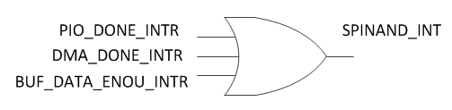
Figure 16-4 SPINAND Interrupt Tree
SPI interrupt status register (Group 87.18 spi_intr_sts) description.
...
87.2 SPI Page Address Regsister (spi page addr)
Address: 0x9C002B88
Reset: 0x0
| Field Name | Bit | Access | Description |
| PAGE ADDR BYTE3 | 31:24 | RW | Page Address[31:24] to be send to SPI DEVICE |
| PAGE ADDR BYTE2 | 23:16 | RW | Page Address[23:16] to be send to SPI DEVICE |
| PAGE ADDR BYTE1 | 15:8 | RW | Page Address[15:8] to be send to SPI DEVICE |
| PAGE ADDR BYTE0 | 7:0 | RW | Page Address[7:0] to be send to SPI DEVICE |
87.3 SPI Data Register (spi data)
Address: 0x9C002B8C
Reset: 0x0
| Field Name | Bit | Access | Description |
| DATA BYTE3 | 31:24 | RW | DATA[31:24] to be write to or read from SPI DEVICE |
| DATA BYTE2 | 23:16 | RW | DATA[23:16] to be write to or read from SPI DEVICE |
| DATA BYTE1 | 15:8 | RW | DATA[15:8] to be write to or read from SPI DEVICE |
| DATA BYTE0 | 7:0 | RW | DATA[7:0] to be write to or read from SPI DEVICE |
87.4 SPI Status Register (spi status)
Address: 0x9C002B90
Reset: 0x0000
| Field Name | Bit | Access | Description |
| Reserved | 31:21 | RO | |
| PRE FETCH BUSY | 20 | RO | Indicate pre-fetch operation ongoing |
| SP2 FLAG CHIP B | 19 | RO | Indicate SP2 mode of chip B |
| SP2 FLAG CHIP A | 18 | RO | Indicate SP2 mode of chip A |
| ADDR 4BYTE FLAG CHIP B | 17 | RO | Indicate 4bytes address mode status of chip B 1: current ADDR mode is 4 bytes; 0: ADDR mode is normal mode. This bit will be set to 1'b1 after EN4B command received, 1'b0 after EX4B command received. |
| ADDR 4BYTE FLAG CHIP A | 16 | RO | Indicate 4bytes address mode status of chip A 1: current ADDR mode is 4 bytes; 0: ADDR mode is normal mode. This bit will be set to 1'b1 after EN4B command received, 1'b0 after EX4B command received. |
| Reserved | 15:8 | RO | Default to be zero |
| FLASH STATUS | 7:0 | RO | Status feed back from SPI DEVICE |
87.5 SPI Configuration1 Register (spi auto cfg)
Address: 0x9C002B94
Reset: 0x3B00
...
87.10 SPI Buffer Address Register (spi buf addr)
Address: 0x9C002BA8
Reset: 0x0000
| Field Name | Bit | Access | Description |
| Reserved | 31:22 | RO | Default to be zero |
| BUF RADDR | 21:16 | RW | SPI DATA64 read address User can define the start read address of data buffer by setting BUF RADDR. |
| Reserved | 15:6 | RO | Default to be zero |
| BUF WADDR | 5:0 | RW | SPI DATA64 write address BUF WADDR will increase by 2 when every writing of SPI DATA64. User can define the start write address of data buffer by setting BUF WADDR. |
87.11 SPI Status2 Register (spi status 2)
Address: 0x9C002BAC
Reset: 0x0000
...
87.13 Memory Data Address (mem data addr)
Address: 0x9C002BB4
Reset: 0x0000
| Field Name | Bit | Access | Description |
| MEM DATA ADDR | 31:0 | RW | Memory Data Address DMA data start address |
87.14 Memory Data Address (mem parity addr)
Address: 0x9C002BB8
Reset: 0x0000
| Field Name | Bit | Access | Description |
| MEM PARITY ADDR | 31:0 | RW | Memory Parity Address DMA parity data start address |
87.15 SPI Column Page Address (spi col addr)
Address: 0x9C002BBC
Reset: 0x0000
| Field Name | Bit | Access | Description |
| Reserved | 31:16 | RO | Default to be zero |
| COL ADDR BYTE1 | 15:8 | RW | SPI Column Addr Column Address[15:8] to be send to SPI device |
| COL ADDR BYTE0 | 7:0 | RW | SPI Column Addr Column Address[7:0] to be send to SPI device |
87.16 SPI BCH configuration Register (spi bch)
Address: 0x9C002BC0
Reset: 0x0000
...