9.1. Power On Sequence
...
Figure 9-1 Power On Sequence
Parameter | Symbol | Min | Typ. | Max. | Units |
XTAL clock output stable time | TXTAL | 5 | - | - | us |
AO33V power on timing range | TAO33VPON | 0 | - | 5 | ms |
VDD33 power on timing range | TVDD33PON | 0 | - | 5 | ms |
Operation mode configure time after AO33V and VDD33 power ready (include internal core power ramp up time and reset circuit time cost) | TMODE | 15 | - | - | ms |
9.2. Power Down Sequence
...
Figure 9-2 Power Down Sequence
9.3. Reset State
There are 3 physically event to trigger chip reset.
...
PORPULSE | PORCONST | |
AVDD33/DVDD12 < Vtrip | '1' | ‘0’ |
AVDD33/DVDD12 > Vtrip | '0' | '1' |
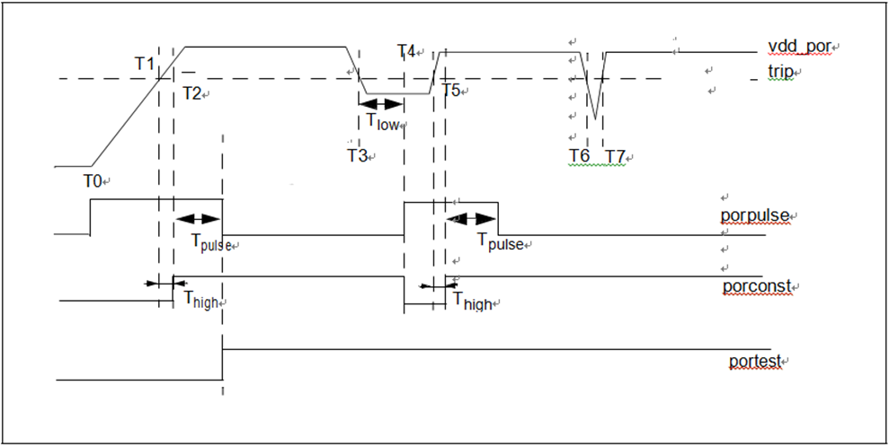
Figure
...
9-3 POR Timing
Parameter | Symbol | Min | Typ.[1] | Max. | Units |
trip-level | |||||
high trip-level | Vtrip_high | 0.70 | 0.80 | 0.90 | V |
low trip-level | Vtrip_low | 0.65 | 0.75 | 0.85 | V |
difference between high and low trip- level | HLtrip_diff | 50 | 70 | 100 | mV |
timing | |||||
time vdd_por has to be above Vtrip_high[3] before porconst will be ‘1’ | Thigh | 2 | µs | ||
time vdd_por has to be below Vtrip_low[4] before porconst will be ‘0’ | Tlow | 11 | µs | ||
time porpulse will be ‘1’ after vdd_por > Vtrip_high | Tpulse | 200 | ns | ||
...
External Reset connects to a button on PCB. Press the button can reset the whole chip to force the whole system to restart. If external reset signal rises through VT+ and keeps high time longer than TRSTH, then internal reset signal de-asserts. If external reset signal falls through VT-, and keeps low time longer TRSTL, then internal reset signal asserts.
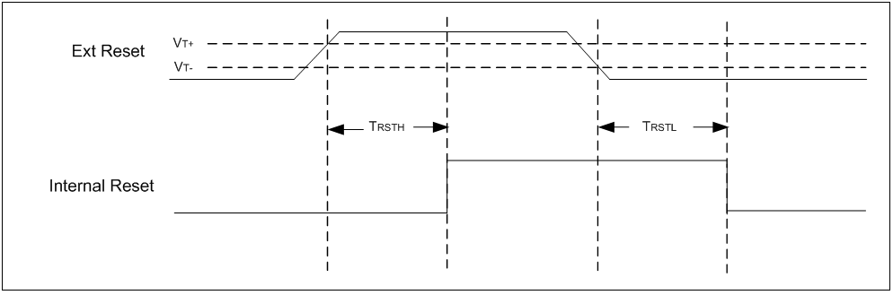
Figure 9-4 External Reset Timing
Parameter | Symbol | Min | Typ. | Max. | Units |
trip-level | |||||
Low to High Threshold Point | VT+ | 1.51 | 1.61 | 1.67 | V |
High to Low Threshold Point | VT- | 0.92 | 0.98 | 1.02 | |
timing | |||||
Reset keep High Time | TRSTH | 1 | µs | ||
Reset keep Low Time | TRSTL | 1 | µs | ||
...
When 1.5V/ 1.2V/ 0.9V voltage is lower than the setting reference voltage, reset signal will be assert to reset the whole chip.
...
Figure 9-5 Low Voltage Detect Timing
Parameter | Symbol | Min | Typ. | Max. | Units |
0.9V Low Voltage duration | TLVD09 | 8 | µs | ||
1.2V Low Voltage duration | TLVD12 | 8 | µs | ||
1.5V Low Voltage duration | TLVD15 | 16 | µs |
...