...
Figure 9-1 Power On Sequence
Parameter | Symbol | Min | Typ. | Max. | Units |
XTAL clock output stable time | TXTAL | 5 | - | - | us |
AO33V power on timing range | TAO33VPON | 0 | - | 5 | ms |
VDD33 power on timing range | TVDD33PON | 0 | - | 5 | ms |
Operation mode configure time after AO33V and VDD33 power ready (include internal core power ramp up time and reset circuit time cost) | TMODE | 15 | - | - | ms |
9.2. Power Down Sequence
...
Figure 9-2 Power Down Sequence
...
To have a better understanding of the functionality of the POR, see Figure 7. In this figure, a possible curve of AVDD33/DVDD12 is given with a dip at T3-T5 and a dip at T6-T7. At T0 the POR, porpulse, will start off with a '1' (= Voh). At T1 the detector passes through the triplevel, porconst becomes '1' after Thigh. A delay element will add an- other Tpulse before porpulse drops to '0'. This is done to make sure that the length of the generated detector pulse, porpulse, is large enough to reset asynchronous flip-flops. If the dip is too short (T7-T6 < Tlow) porpulse will not react and will stay low.
PORPULSE | PORCONST | |
AVDD33/DVDD12 < Vtrip | '1' | ‘0’ |
AVDD33/DVDD12 > Vtrip | '0' | '1' |
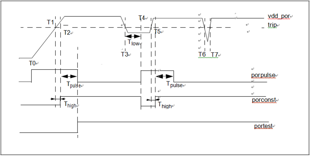
Figure 9-3 POR Timing
Parameter | Symbol | Min | Typ.[1] | Max. | Units |
trip-level | |||||
high trip-level | Vtrip_high | 0.70 | 0.80 | 0.90 | V |
low trip-level | Vtrip_low | 0.65 | 0.75 | 0.85 | V |
difference between high and low trip- level | HLtrip_diff | 50 | 70 | 100 | mV |
timing | |||||
time vdd_por has to be above Vtrip_high[3] before porconst will be ‘1’ | Thigh | 2 | µs | ||
time vdd_por has to be below Vtrip_low[4] before porconst will be ‘0’ | Tlow | 11 | µs | ||
time porpulse will be ‘1’ after vdd_por > Vtrip_high | Tpulse | 200 | ns | ||
...
External Reset
External Reset connects to a button on PCB. Press the button can reset the whole chip to force the whole system to restart. If The external reset is ACTIVE LOW meaning that asserting external reset LOW, will cause the entire system to reset. If the external reset signal rises through VT+ and keeps high HIGH time longer than TRSTH, then the internal reset signal de-asserts. If external reset signal falls through VT-, and keeps low LOW time longer TRSTL, then internal reset signal asserts.
...
Figure 9-4 External Reset Timing
Parameter | Symbol | Min | Typ. | Max. | Units |
trip-level | |||||
Low to High Threshold Point | VT+ | 1.51 | 1.61 | 1.67 | V |
High to Low Threshold Point | VT- | 0.92 | 0.98 | 1.02 | |
timing | |||||
Reset keep High Time | TRSTH | 1 | µs | ||
Reset keep Low Time | TRSTL | 1 | µs | ||
n LVD
When 1.5V/ 1.2V/ 0.9V voltage is lower than the setting reference voltage, reset signal will be assert to reset the whole chip.
...
Figure 9-5 Low Voltage Detect Timing
Parameter | Symbol | Min | Typ. | Max. | Units |
0.9V Low Voltage duration | TLVD09 | 8 | µs | ||
1.2V Low Voltage duration | TLVD12 | 8 | µs | ||
1.5V Low Voltage duration | TLVD15 | 16 | µs |