1617.1 Introduction
This section describes the SPI_NOR Controller and its function. The SPI_NOR Controller is used to transmit or receive data with SPI_NOR device. The control registers locate at RGST Table Group 22&23 which memory map address are 0x9C000B00~0x9C000BFF. The SPINOR controller has below features.
- Support 32-bit AXI master bus for transferring data between controller and dram for DMA mode
- Exchange to 32-bit AXI Slave bus from 32-bit OCP bus
- Support auto multi page read
- Support auto multi page program
- Support SPI_CLK is divided from CLK_SPI, and frequency division coefficient is 1/2, 1/4, 1/6, 1/8, 1/16, 1/24, 1/32
...
17.2 Function Diagram
A generalized function diagram of SPINOR is shown in Figure 1617-1. SPI_NOR_BCHIF is revered for SPI_NOR Controller. BCH function is only useful for SPI_NAND controller.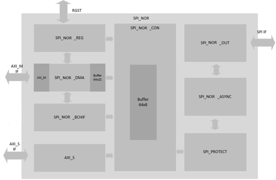
Figure 1617-1 SPI NOR Functional Blocks
- SPI_NOR_REG: This block is used for register configure.
- SPI_NOR_DMA: Support 32-bit AXI master bus to read/write data between controller and dram for DMA mode.
- SPI_NOR_CON: This block is used for controlling the operation flow
- SPI_NOR_OUT: SPI interface with external SPI device.
- SPI_NOR
_ASYNC: For async information between SPI_NOR_CON and SPI_NOR_OUTAnchor _GoBack _GoBack - SPI_NOR_AXI_S: Exchange to 32-bit AXI Slave bus from 32-bit OCP bus.
- SPI_PROTECT: This block is used for protect the configuration regions of SPI_NOR flash size.
...
17.3 Data Control Timing
SPI_NOR Controller TX timing: The TX output start timing decides by spi_timing[0] which is bit0 of Group 22.1 spi_timing register. When spi_timing[0]=1 , TX will advance one system clock cycle to send data. Please refer to figure 1617-2.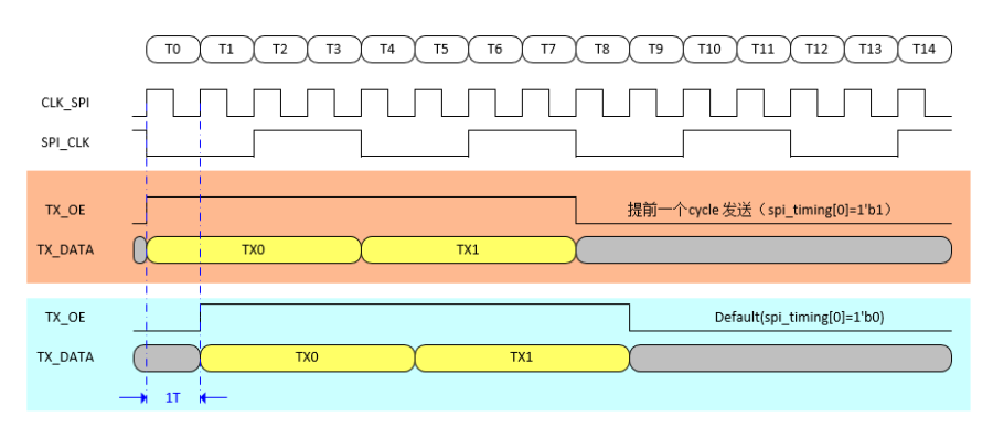
Figure 1617-2 TX timing chart
SPI_NOR Controller RX timing: The RX timing can be fine tune by spi_timing[3:1] which is bit[3:1] of Group 22.1 spi_timing register.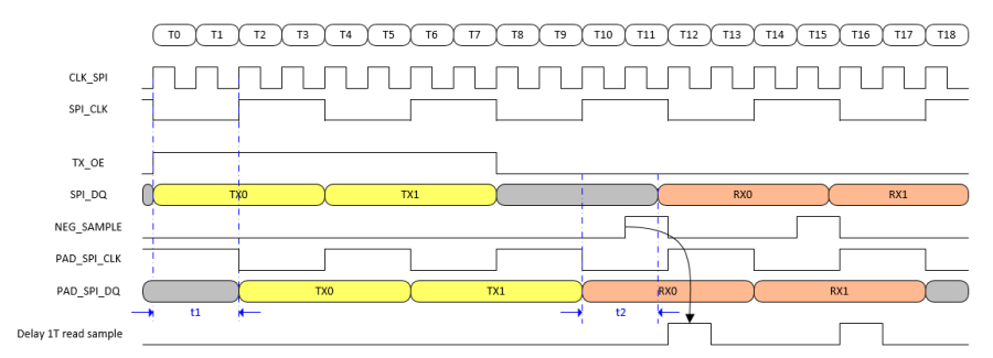
- Figure 1617-3 RX timing chart
- If the pad TX delay is t1,than from device to response data until SPI Controller receive data the delay is t2.
- NEG_SAMPLE is spi_controller default sample point
- As above figure,controller can't get correct data in the default sample point,user can fine tune spi_timing[3:1] to get correct read timing. For example, in figure 1617-3 set spi_timing[3:1]=1 can get correct sample data.
...
17.4 SPI NOR Interrupts
The SPINOR interrupt events are connected to the same interrupt vector, please refer to figure 1617-4. These events generate an interrupt if the corresponding "Mask Bit" isn't set. The mask control register is in Group 22.17. The interrupt status register is in Group 22.18. SPI_NOR controller interrupt is a level signal. It supports three kinds of interrupt status. If one interrupt mask enable, this interrupt will only update the status, the SPINOR_INT will not be set. 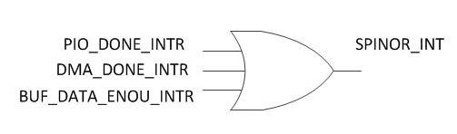
Figure 1617-4 SPINOR Interrupt Tree
SPI interrupt status register (Group 22.18 spi_intr_sts) description.
- PIO_DONE_INTR: When PIO mode transfer finished, spi_intr_sts[2] will be high. Software write 1 to clean this bit.
- DMA_DONE_INTR: spi_intr_sts[1] indicate the current dma operation is done. Software can write 1 to clear this bit
- BUF_DATA_ENOU_INTR: spi_intr_sts[0] indicate the number of data received from flash has reached the setting amount. Software can write 1 to clear this bit. The amount is set in spi_cfg0[21] which is bit 21 of Group 22.6 register. Set spi_cfg0[21]=1, the buffer size is 32byte. Set spi_cfg0[21]=0, the buffer size is 64byte.
...
17.5 Registers Map
...
17.5.1 Registers Memory Map
Address | Group No. | Register Name | Register Description |
|---|---|---|---|
0x9C000B00 | G22.0 | Spi_Ctrl | SPI control Register |
0x9C000B04 | G22.1 | Spi_timing | SPI timing Register |
0x9C000B08 | G22.2 | Spi_page_addr | SPI Page Address Register |
0x9C000B0C | G22.3 | Spi_data | SPI Data Register |
0x9C000B10 | G22.4 | Spi_status | SPI Status Register |
0x9C000B14 | G22.5 | Spi_auto_cfg | SPI Auto Mode Configuration Register |
0x9C000B18 | G22.6 | Spi_cfg0 | SPI Configuration0 Register |
0x9C000B1C | G22.7 | Spi_cfg1 | SPI Configuration1 Register |
0x9C000B20 | G22.8 | Spi_cfg2 | SPI Configuration2 Register |
0x9C000B24 | G22.9 | Spi_data_64 | SPI Data Buffer Register |
0x9C000B28 | G22.10 | Spi_buf_addr | SPI Buffer Address Register |
0x9C000B2C | G22.11 | Spi_status_2 | SPI Status2 Register |
0x9C000B30 | G22.12 | Spi_err_status | SPI Error Status |
0x9C000B34 | G22.13 | Mem_data_addr | Memory Data Address |
0x9C000B38 | G22.14 | Mem_parity_addr | Memory Parity Address For SPI_NOR is reserved. |
0x9C000B3C | G22.15 | Spi_col_addr | SPI Column Page Address For SPI_NOR is reserved. |
0x9C000B40 | G22.16 | Spi_bch | SPI BCH Configuration Register For SPI_NOR is reserved. |
0x9C000B44 | G22.17 | Spi_intr_msk | SPI Interrupt Mask Register |
0x9C000B48 | G22.18 | Spi_intr_sts | SPI Interrupt Status Register |
0x9C000B4C | G22.19 | Spi_page_size | SPI Device Page Size |
...
Address | Group No. | Register Name | Register Description |
|---|---|---|---|
0x9C000B80 | G23.0 | Spi_protect_cfg | Protect Configuration Register |
0x9C000B84 | G23.1 | Spi_region0_start_addr | Protection Region0 Start Address |
0x9C000B88 | G23.2 | Spi_region0_size | Size of Protection Region0 |
0x9C000B8C | G23.3 | Spi_region1_start_addr | Protect Region1 Start Address |
0x9C000B90 | G23.4 | Spi_region1_size | Size of Protection Region1 |
0x9C000B94 | G23.5 | Spi_region2_start_addr | Protect Region2 Start Address |
0x9C000B98 | G23.6 | Spi_region2_size | Size of Protection Region2 |
0x9C000B9C | G23.7 | Spi_scramble1 | SPI Scramble1 Register |
0x9C000BA0 | G23.8 | Spi_scramble2 | SPI Scramble2 Register |
0x9C000BA4 | G23.9 | Spi_scramble3 | SPI Scramble3 Register |
...
17.5.2 Registers Description
RGST Table Group 22SPI Controller Registers
22.0 SPI Control Register (spi ctrl)
Address: 0x9C000B00
Reset: 0x0117 0003
...