17. SPI NOR
- edwin.chiu (Unlicensed)
17.1 Introduction
This section describes the SPI_NOR Controller and its function. The SPI_NOR Controller is used to transmit or receive data with SPI_NOR device. The control registers locate at RGST Table Group 22&23 which memory map address are 0x9C000B00~0x9C000BFF. The SPINOR controller has below features.
- Support 32-bit AXI master bus for transferring data between controller and dram for DMA mode
- Exchange to 32-bit AXI Slave bus from 32-bit OCP bus
- Support auto multi page read
- Support auto multi page program
- Support SPI_CLK is divided from CLK_SPI, and frequency division coefficient is 1/2, 1/4, 1/6, 1/8, 1/16, 1/24, 1/32
17.2 Function Diagram
A generalized function diagram of SPINOR is shown in Figure 17-1. SPI_NOR_BCHIF is revered for SPI_NOR Controller. BCH function is only useful for SPI_NAND controller.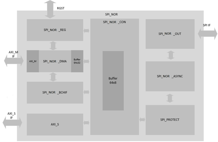
Figure 17-1 SPI NOR Functional Blocks
- SPI_NOR_REG: This block is used for register configure.
- SPI_NOR_DMA: Support 32-bit AXI master bus to read/write data between controller and dram for DMA mode.
- SPI_NOR_CON: This block is used for controlling the operation flow
- SPI_NOR_OUT: SPI interface with external SPI device.
- SPI_NOR _ASYNC: For async information between SPI_NOR_CON and SPI_NOR_OUT
- SPI_NOR_AXI_S: Exchange to 32-bit AXI Slave bus from 32-bit OCP bus.
- SPI_PROTECT: This block is used for protect the configuration regions of SPI_NOR flash size.
17.3 Data Control Timing
SPI_NOR Controller TX timing: The TX output start timing decides by spi_timing[0] which is bit0 of Group 22.1 spi_timing register. When spi_timing[0]=1 , TX will advance one system clock cycle to send data. Please refer to figure 17-2.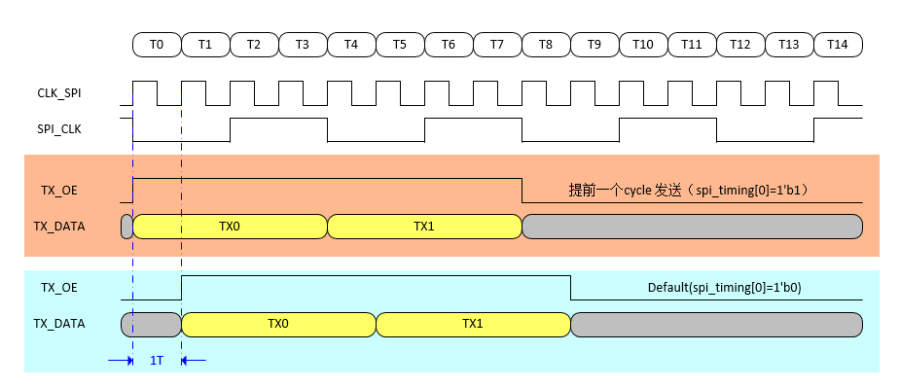
Figure 17-2 TX timing chart
SPI_NOR Controller RX timing: The RX timing can be fine tune by spi_timing[3:1] which is bit[3:1] of Group 22.1 spi_timing register.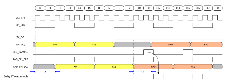
- Figure 17-3 RX timing chart
- If the pad TX delay is t1,than from device to response data until SPI Controller receive data the delay is t2.
- NEG_SAMPLE is spi_controller default sample point
- As above figure,controller can't get correct data in the default sample point,user can fine tune spi_timing[3:1] to get correct read timing. For example, in figure 17-3 set spi_timing[3:1]=1 can get correct sample data.
17.4 SPI NOR Interrupts
The SPINOR interrupt events are connected to the same interrupt vector, please refer to figure 17-4. These events generate an interrupt if the corresponding "Mask Bit" isn't set. The mask control register is in Group 22.17. The interrupt status register is in Group 22.18. SPI_NOR controller interrupt is a level signal. It supports three kinds of interrupt status. If one interrupt mask enable, this interrupt will only update the status, the SPINOR_INT will not be set. 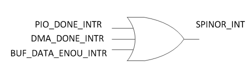
Figure 17-4 SPINOR Interrupt Tree
SPI interrupt status register (Group 22.18 spi_intr_sts) description.
- PIO_DONE_INTR: When PIO mode transfer finished, spi_intr_sts[2] will be high. Software write 1 to clean this bit.
- DMA_DONE_INTR: spi_intr_sts[1] indicate the current dma operation is done. Software can write 1 to clear this bit
- BUF_DATA_ENOU_INTR: spi_intr_sts[0] indicate the number of data received from flash has reached the setting amount. Software can write 1 to clear this bit. The amount is set in spi_cfg0[21] which is bit 21 of Group 22.6 register. Set spi_cfg0[21]=1, the buffer size is 32byte. Set spi_cfg0[21]=0, the buffer size is 64byte.
17.5 Registers Map
17.5.1 Registers Memory Map
Address | Group No. | Register Name | Register Description |
|---|---|---|---|
0x9C000B00 | G22.0 | Spi_Ctrl | SPI control Register |
0x9C000B04 | G22.1 | Spi_timing | SPI timing Register |
0x9C000B08 | G22.2 | Spi_page_addr | SPI Page Address Register |
0x9C000B0C | G22.3 | Spi_data | SPI Data Register |
0x9C000B10 | G22.4 | Spi_status | SPI Status Register |
0x9C000B14 | G22.5 | Spi_auto_cfg | SPI Auto Mode Configuration Register |
0x9C000B18 | G22.6 | Spi_cfg0 | SPI Configuration0 Register |
0x9C000B1C | G22.7 | Spi_cfg1 | SPI Configuration1 Register |
0x9C000B20 | G22.8 | Spi_cfg2 | SPI Configuration2 Register |
0x9C000B24 | G22.9 | Spi_data_64 | SPI Data Buffer Register |
0x9C000B28 | G22.10 | Spi_buf_addr | SPI Buffer Address Register |
0x9C000B2C | G22.11 | Spi_status_2 | SPI Status2 Register |
0x9C000B30 | G22.12 | Spi_err_status | SPI Error Status |
0x9C000B34 | G22.13 | Mem_data_addr | Memory Data Address |
0x9C000B38 | G22.14 | Mem_parity_addr | Memory Parity Address For SPI_NOR is reserved. |
0x9C000B3C | G22.15 | Spi_col_addr | SPI Column Page Address For SPI_NOR is reserved. |
0x9C000B40 | G22.16 | Spi_bch | SPI BCH Configuration Register For SPI_NOR is reserved. |
0x9C000B44 | G22.17 | Spi_intr_msk | SPI Interrupt Mask Register |
0x9C000B48 | G22.18 | Spi_intr_sts | SPI Interrupt Status Register |
0x9C000B4C | G22.19 | Spi_page_size | SPI Device Page Size |
Address | Group No. | Register Name | Register Description |
|---|---|---|---|
0x9C000B80 | G23.0 | Spi_protect_cfg | Protect Configuration Register |
0x9C000B84 | G23.1 | Spi_region0_start_addr | Protection Region0 Start Address |
0x9C000B88 | G23.2 | Spi_region0_size | Size of Protection Region0 |
0x9C000B8C | G23.3 | Spi_region1_start_addr | Protect Region1 Start Address |
0x9C000B90 | G23.4 | Spi_region1_size | Size of Protection Region1 |
0x9C000B94 | G23.5 | Spi_region2_start_addr | Protect Region2 Start Address |
0x9C000B98 | G23.6 | Spi_region2_size | Size of Protection Region2 |
0x9C000B9C | G23.7 | Spi_scramble1 | SPI Scramble1 Register |
0x9C000BA0 | G23.8 | Spi_scramble2 | SPI Scramble2 Register |
0x9C000BA4 | G23.9 | Spi_scramble3 | SPI Scramble3 Register |
17.5.2 Registers Description
RGST Table Group 22SPI Controller Registers
22.0 SPI Control Register (spi ctrl)
Address: 0x9C000B00
Reset: 0x0117 0003
| Field Name | Bit | Access | Description |
| SPI BUSY | 31 | RO | SPI controller busy 0: SPI DEVICE is in IDLE state 1: SPI DEVICE is in busy |
| Reserved | 30 | RO | Default to be zero |
| PAGE ACCESS | 29 | RW | Page access mode 0: SPI CS B raise when each read command end 1: SPI CS B keep in page mode when read command end and read command is identified (OCP bus read or auto identify customized read command) |
| AUTO MODE | 28 | RW | Auto to page program and page read Auto mode: CPU will enable controller once to finish a page program or a page read operation. |
| AUTO CMD EN | 27 | RW | Auto Command Enable 1'b0:usedefault cmd(PRGM EXE:10h, READ TO CACHE: 13h) |
AUTO 4BYTE ADDR EN | 26 | RW | Auto do opearation with 4 bytes addr mode |
FLASH B SEL | 25 | RW | Select SPI FLASH Chip B |
FLASH A SEL | 24 | RW | Select SPI FLASH Chip A |
USEABLE DQ | 23:20 | RW | Useable Serial Interface data bits |
AUTO SPI WEL EN | 19 | RW | Auto write enable latch |
SCK MODE | 18:16 | RW | SPI clock frequency division selection |
| MULTI CMD | 15:8 | RW | Multi command for auto mode cmd or customer cmd to be send to SPI DEVICE Function 1:used for auto mode, user can define PRGM EXE or READ TO CACHE cmd. Function 2: used to define customer command. |
SPI NAND EN | 7 | RW | SPI NAND enable signal |
CUSTOMER DATA LEN SRC | 6:4 | RW | Byte length for SPI data |
Reserved | 3 | RO | Default to be zero |
|
|
|
|
CUST ADDR LEN | 1:0 | RW | Byte length for SPI address |
22.1 SPI Timing Register (spi timing)
Address: 0x9C000B04
Reset: 0x012A 0000
| Field Name | Bit | Access | Description |
| Reserved | 31:27 | RO | Default to be zero |
| CS SH CYC | 26:22 | RW | SPI CS B setup cycles and hold cycles For example, when CLK SPI=400MHZ, the setting value = |
CS DISACTIVE CYC | 21:16 | RW | SPI CS B disactive cycles |
Reserved | 15:4 | RO | Default to be zero |
|
|
|
|
WRITE TIMING SEL | 0 | RW | SPI CLK output timing option |
22.2 SPI Page Address Regsister (spi page addr)
Address: 0x9C000B08
Reset: 0x0
| Field Name | Bit | Access | Description |
| PAGE ADDR BYTE3 | 31:24 | RW | Page Address[31:24] to be send to SPI DEVICE |
| PAGE ADDR BYTE2 | 23:16 | RW | Page Address[23:16] to be send to SPI DEVICE |
| PAGE ADDR BYTE1 | 15:8 | RW | Page Address[15:8] to be send to SPI DEVICE |
| PAGE ADDR BYTE0 | 7:0 | RW | Page Address[7:0] to be send to SPI DEVICE |
22.3 SPI Data Register (spi data)
Address: 0x9C000B0C
Reset: 0x0
Field Name | Bit | Access | Description |
| DATA BYTE3 | 31:24 | RW | DATA[31:24] to be write to or read from SPI DEVICE |
| DATA BYTE2 | 23:16 | RW | DATA[23:16] to be write to or read from SPI DEVICE |
| DATA BYTE1 | 15:8 | RW | DATA[15:8] to be write to or read from SPI DEVICE |
| DATA BYTE0 | 7:0 | RW | DATA[7:0] to be write to or read from SPI DEVICE |
22.4 SPI Status Register (spi status)
Address: 0x9C000B10
Reset: 0x0000
| Field Name | Bit | Access | Description |
| Reserved | 31:21 | RO | |
| PRE FETCH BUSY | 20 | RO | Indicate pre-fetch operation ongoing |
| SP2 FLAG CHIP B | 19 | RO | Indicate SP2 mode of chip B |
| SP2 FLAG CHIP A | 18 | RO | Indicate SP2 mode of chip A |
| ADDR 4BYTE FLAG CHIP B | 17 | RO | Indicate 4bytes address mode status of chip B 1: current ADDR mode is 4 bytes; 0: ADDR mode is normal mode. This bit will be set to 1'b1 after EN4B command received, 1'b0 after EX4B command received. |
ADDR 4BYTE FLAG CHIP A | 16 | RO | Indicate 4bytes address mode status of chip A |
1: current ADDR mode is 4 bytes; | |||
0: ADDR mode is normal mode. | |||
This bit will be set to 1'b1 after EN4B command received, | |||
|
|
| 1'b0 after EX4B command received. |
|
|
|
|
22.5SPI Configuration1 Register (spi auto cfg)
Address:0x9C000B14
Reset:0x3B00
| Field Name | Bit | Access | Description |
| READ FROM CACHE | 31:24 | RW | Read from cache command When use the auto mode or DMA function, user can set READ FROM CACHE command. |
| CONTINUE MODE | 23 | RW | Winbond Read continue Mode Enable 1'b0: Disable read continue mode. 1'b1: Enable read continue mode. |
| PRE FETCH EN | 22 | RW | Pre-fetch enable 0: disable pre-fetch function 1: enable pre-fetch fucntion This bit afffect OCP/CUST read command |
| REG SPI EN | 21 | Other | customer command enable/disable 0: customer command has been finished or customer com- mand is not enabled 1: customer command is enabled and triggered Note: User can not set this bit to disable if it is ever setted to enable. It will go to disable after the current executing command is finished. |
| AUTO RD CMD EN | 20 | RW | User defined READ FROM CACHE command enable 0: use default READ FROM CACHE read command 1: use user defined command. |
CHECK DEVICE OIP | 19 | RW | Check whether device is busy or not |
AUTO RDSR EN | 18 | RW | Auto read status register enable |
DMA OWNER | 17 | RW | DMA Owner bit |
DUMMY OUT | 16 | RW | Data in/out selection in dummy cycles |
PRGM LOAD | 15:8 | RW | Page Program Load data command |
Reserved | 7:3 | RO | Default to be zero |
|
|
|
|
AUTO WREN 1 | 1 | RW | Auto WREN before program load |
AUTO WR CMD EN | 0 | RW | User defined PRGM LOAD command enable |
22.6 SPI Configuration0 Register (spi cfg0)
Address: 0x9C000B18
Reset: 0x8 0004
| Field Name | Bit | Access | Description |
| ENHANCE DATA | 31:24 | RW | Enhance data to be send |
| ENDIAN MODE | 23 | RW | Endian mode select for OCP 0: Big endian 1: Little endian |
| DQ BIT SWITCH | 22 | RW | Switch serial data pin DQ0 and DQ1 0: DQ1 is high bit and DQ0 is low bit when transferred mode equal to 2 1: DQ0 is high bit and DQ1 is low bit when transferred mode equal to 2 |
| BUF DATA NUM SEL | 21 | RW | Buffer Data Number Select 1'b1: When receive 32Bytes data into buffer 1'b0: When receive 64Bytes data into buffer There will issue a interrupt after reading the amount of data. But SPI NAND won't stop after interrupt. |
| DATA64 EN | 20 | RW | 64-byte customized read/write operation enable 1'b0: use SPI DATA. 1'b1: use SPI DATA64. |
| SPI TRS MODE | 19 | RW | Transferring mode for auto WREN and RDSR 0: using SPI CFG4,5,6,7 setting 1: SPI mode transferred |
| ENHANCE 8BITS SEL | 18 | RW | Enhance Bits to be transferred 0: 4 bits to be transferred(SPI CFG3[15:12]) 1: 8 bits to be transferred |
| SCK IDLE | 17 | RW | SPI CLK mode 0: SPI CLK high active at idle state 1: SPI CLK low active at idle state |
| Reserved | 16 | RO | Default to be zero |
| DATA LEN | 15:0 | Other | Byte length for SPI data Indicate the number of data will be programmed to flash or read from flash no matter under normal/auto mode or DMA mode. |
22.7 SPI Configuration1 Register (spi cfg1)
Address: 0x9C000B1C
Reset: 0x0015 0095
| Field Name | Bit | Access | Description |
| Reserved | 31:30 | RO | Default to be zero |
| CUST DUMMY CYC | 29:24 | RW | Serial interface dummy cycle The range is from 0 to 63. e |
| CUST ENHANCE BIT | 23:22 | RW | Serial interface enhance data mode 0: no need transferred 1: 1 bit mode 2: 2 bit mode 3: 4 bit mode |
| CUST DATA BIT | 21:20 | RW | Serial interface data mode 0: no need transferred 1: 1 bit mode 2: 2 bit mode 3: 4 bit mode |
| CUST ADDR BIT | 19:18 | RW | Serial interface address mode 0: no need transferred 1: 1 bit mode 2: 2 bit mode 3: 4 bit mode |
| CUST CMD BIT | 17:16 | RW | Serial interface command mode 0: no need transferred 1: 1 bit mode 2: 2 bit mode 3: 4 bit mode |
| Reserved | 15:8 | RO | Default to be zero |
| CUST DATA DQ IEN | 7:6 | RW | Customized DATA bit input enable, only affect 1bit mode 0: input disable 1: DQ0 input enable 2: DQ1 input enable |
CUST DATA DQ OEN | 5:4 | RW | Customized DATA bit output enable, only affect 1bit mode |
CUST ADDR DQ OEN | 3:2 | RW | Customized ADDR bit output enable, only affect 1bit mode |
CUST CMD DQ OEN | 1:0 | RW | Customized CMD bit output enable, only affect 1bit mode |
22.8 SPI Configuration2 Register (spi cfg2)
Address: 0x9C000B20
Reset: 0x0015 0095
| Field Name | Bit | Access | Description |
| Reserved | 31:30 | RO | Default to be zero |
| DMA DUMMY CYC | 29:24 | RW | Serial interface dummy cycle The range is from 0 to 63. e |
| DMA ENHANCE BIT | 23:22 | RW | Serial interface enhance data mode 0: no need transferred 1: 1 bit mode 2: 2 bit mode 3: 4 bit mode |
| DMA DATA BIT | 21:20 | RW | Serial interface data mode 0: no need transferred 1: 1 bit mode 2: 2 bit mode 3: 4 bit mode |
DMA ADDR BIT | 19:18 | RW | Serial interface address mode |
DMA CMD BIT | 17:16 | RW | Serial interface command mode |
Reserved | 15:8 | RO | Default to be zero |
|
|
|
|
DMA DATA DQ OEN | 5:4 | RW | Customized DATA bit output enable, only affect 1bit mode |
DMA ADDR DQ OEN | 3:2 | RW | Customized ADDR bit output enable, only affect 1bit mode |
DMA CMD DQ OEN | 1:0 | RW | Customized CMD bit output enable, only affect 1bit mode |
22.9 SPI Data Buffer Regsiter (spi data 64)
Address: 0x9C000B24
Reset: 0x0000
| Field Name | Bit | Access | Description |
| DATA64 BYTE3 | 31:24 | RW | data[31:24] to be write to or read from SPI DEVICE Repeated read this register achieve read data from data buffer when reading from SPI DEVICE, repeated write this register achieve write data to data buffer when any time |
| DATA64 BYTE2 | 23:16 | RW | data[23:16] to be write to or read from SPI DEVICE Repeated read this register achieve read data from data buffer when reading from SPI DEVICE, repeated write this register achieve write data to data buffer when any time |
| DATA64 BYTE1 | 15:8 | RW | data[15:8] to be write to or read from SPI DEVICE Repeated read this register achieve read data from data buffer when reading from SPI DEVICE, repeated write this register achieve write data to data buffer when any time |
| DATA64 BYTE0 | 7:0 | RW | data[7:0] to be write to or read from SPI DEVICE Repeated read this register achieve read data from data buffer when reading from SPI DEVICE, repeated write this register achieve write data to data buffer when any time |
22.10SPI Buffer Address Register (spi buf addr)
Address:0x9C000B28
Reset:0x0000
| Field Name | Bit | Access | Description |
| Reserved | 31:22 | RO | Default to be zero |
| BUF RADDR | 21:16 | RW | SPI DATA64 read address User can define the start read address of data buffer by setting BUF RADDR. |
| Reserved | 15:6 | RO | Default to be zero |
| BUF WADDR | 5:0 | RW | SPI DATA64 write address BUF WADDR will increase by 2 when every writing of SPI DATA64. User can define the start write address of data buffer by setting BUF WADDR. |
22.11 SPI Status2 Register (spi status 2)
Address: 0x9C000B2C
Reset: 0x2000
| Field Name | Bit | Access | Description |
| Reserved | 31:23 | RO | Default to be zero |
| DMA SUB ST | 22:20 | RO | DMA sub state 0x0: AXI IDLE 0x1: AXI WR INFO 0x2: AXI WR DATA 0x3: AXI RD INFO 0x4: AXI RD DATA |
| DMA MAIN ST | 19:18 | RO | DMA main state 0x0: DMA IDLE 0x1: DMA DATA 0x2: DMA PARITY |
| BCH ST | 17:16 | RO | DMA main state 0x0: IDLE 0x1: ENCODE 0x2: DECODE |
| SPI SRAM ST | 15:13 | RO | Status of SRAM [0]: SRAM conflict, both OCP and customzied read/write at the same time [1]: SRAM empty [2]: SRAM full |
SPI CON ST | 12:8 | RU | Status of block SPI CON |
SPI OUT ST | 7:4 | RU | Status of block SPI OUT |
SPI AXIS ST | 3:0 | RO | Status of block SPI AXIS |
22.12 SPI Controller Error Status Register (spi err status)
Address: 0x9C000B30
Reset: 0x0000
Field NameBitAccessDescription
| Field Name | Bit | Access | Description |
| Reserved | 15:3 | RO | |
TWO CHIP SEL ERR | 2 | W1C | Error flag about two chip selected |
NO CHIP SEL ERR | 1 | W1C | Error flag about no chip selected |
CUS DATA64 OVERFLOW ERR | 0 | W1C | Error flag about DATA64 write data overflow to inner |
22.13 Memory Data Address (mem data addr)
Address: 0x9C000B34
Reset: 0x0000
| Field Name | Bit | Access | Description |
| MEM DATA ADDR | 31:0 | RW | Memory Data Address DMA data start address |
22.14 Memory Data Address (mem parity addr)
Address: 0x9C000B38
Reset: 0x0000
| Field Name | Bit | Access | Description |
| MEM PARITY ADDR | 31:0 | RW | Memory Parity Address DMA parity data start address |
22.15 SPI Column Page Address (spi col addr)
Address: 0x9C000B3C
Reset: 0x0000
| Field Name | Bit | Access | Description |
Reserved | 31:16 | RO | Default to be zero |
|
|
|
|
COL ADDR BYTE0 | 7:0 | RW | SPI Column Addr |
22.16 SPI BCH configuration Register (spi bch)
Address: 0x9C000B40
Reset: 0x0000
| Field Name | Bit | Access | Description |
| Reserved | 31:16 | RO | Default to be zero |
| BCH DATA LEN | 15:8 | RW | BCH data length per sector For bch data: 0x0: 0Byte parity data per BCH sector 0x1: 1Byte parity data per BCH sector ... 0xff: 255Byte parity data per BCH sector |
| Reserved | 7 | RO | Default to be zero |
| BCH DATA MODE | 6 | RW | BCH data mdoe select 0: 512Byte per BCH. 1: 1k Byte per BCH. |
| BCH ACC | 5 | RW | 32Byte or 16Byte align 0: 32Byte align. 1: 16Byte align. |
| AUTO BCH EN | 4 | RW | Auto BCH function enable Write 1 enable. It will encode data before the page program or decode data during page read. |
| SECTOR NUM | 3:0 | RW | Set the number N of block for BCH N= 0˜15(1˜16 blocks) |
22.17 SPI Interrupt Mask Register (spi intr msk)
Address: 0x9C000B44
Reset: 0x0000
Field Name | Bit | Access | Description | |
Reserved | 31:3 | RO | Default to be zero | |
|
|
|
| |
DMA DONE MASK | 1 | RW | DMA done mask | |
BUF DATA ENOU MASK | 0 | RW | Buffer data enough mask |
22.18 SPI Interrupt Status Register (spi intr sts)
Address: 0x9C000B48
Reset: 0x0000
Field Name | Bit | Access | Description | |
Reserved | 31:3 | RO | Default to be zero | |
|
|
|
| |
DMA DONE INTR | 1 | RW | DMA done interrput | |
BUF DATA ENOU INTR | 0 | RW | Buffer data enough interrupt |
22.19 SPI device page size (spi page size)
Address: 0x9C000B4C
Reset: 0x0000
| Field Name | Bit | Access | Description |
| Reserved | 31:16 | RO | Default to be zero |
| ECC EN | 15 | RW | Device ECC enable 0x1: Device enable ECC, the data can not be stored in spare space. 0x0: Device disable ECC, the data can be stored in spare space. |
| SPARE SIZE LEN | 14:4 | RW | Device Spare Space length 0x0: 0Byte 0x1: 1Byte ... 0x7ff: 2047Byte Note: When SPI NAND, it is spare space in device; when SPI NOR, it is per page size in device |
| Reserved | 3 | RO | Default to be zero |
| PAGE SIZE LEN | 2:0 | RW | Page number select Used for auto mode and DMA mode to count the page number. For 0˜7, indicate 1˜8k Byte data per page. Example: 1. ECC enable: the page size only decide by PAGE SIZE LEN, if PAGE SIZE LEN = 0x1, it indicates 2k Byte per page. 2. ECC disable: if PAGE SIZE LEN=0x1, and the SPARE SIZE LEN = 64Byte, it indicate (2K + 64)Byte per page. |
Group 23SPI Protection/Scramble/Descramble Registers
23.0 Protect Configration Register (spi protect cfg)
Address: 0x9C000B80
Reset: 0x0000
| Field Name | Bit | Access | Description |
| RSV | 31:25 | RO | Reserved |
| ignore block erase | 24 | RW | Ignore Block Erase Command this bit must be set to 1 to avoid the protection region is erased by block-erase in protection mode. Else it should be set to 0. |
| RSV | 23 | RO | Reserved |
| wp2 en | 22 | RW | Write Protect Enable for Region2 This bit can only be written to 1. Write 0 has no effect. 0: normal. The SPI flash can normally be written for pro- tection region2 address. 1: write protection. Address in the protection region2 can not be written. |
| wp1 en | 21 | RW | Write Protect Enable for Region1 This bit can only be written to 1. Write 0 has no effect. 0: normal. The SPI flash can normally be written for pro- tection region1 address. 1: write protection. Address in the protection region1 can not be written. |
| wp0 en | 20 | RW | Write Protect Enable for Region0 This bit can only be written to 1. Write 0 has no effect. 0: normal. The SPI flash can normally be written for pro- tection region0 address. 1: write protection. Address in the protection region0 can not be written. |
| RSV | 19 | RO | Reserved |
rp2 en | 18 | RUW | Read Protect Enable for Region2 |
rp1 en | 17 | RUW | Read Protect Enable for Region1 |
rp0 en | 16 | RUW | Read Protect Enable for Region0 |
RSV | 15:7 | RO | Reserved |
flash size | 6:4 | RUW | SPI Flash Size This field can be normally accessed only when write this field has no effect and read this field return 000: 1M Byte flash memory size. 001: 2M Byte flash memory size 010: 4M Byte flash memory size. 011: 8M Byte flash memory size. 100: 16M Byte flash memory size. 101: 32M Byte flash memory size. |
| RSV | 3:2 | RO | Reserved |
out range wp en | 1 | RUW | Out of Range Write Protect Enable |
out range rp en | 0 | RUW | Out of Range Read Protect Enable |
23.1 Protection Region0 Start Address (spi region0 start addr)
Address: 0x9C000B84
Reset: 0x0000
| Field Name | Bit | Access | Description |
region0 start addr high | 31:16 | RUW | Protection Region0 Start Address[31:16] |
This field can be normally accessed only when rp0 en and | |||
wp0 en are all 0. That is, when rp0 en or wp0 en is 1, | |||
write this field has no effect and read this field returns | |||
{[18:16],[25:22],[31:26],[21:19]}. | |||
region0 start addr low | 15:0 | RUW | Protection Region0 Start Address[15:0] |
This field can be normally accessed only when rp0 en and | |||
wp0 en are all 0. That is, when rp0 en or wp0 en is 1, | |||
write this field has no effect and read this field returns | |||
{[2:0],[9:6],[15:10],[5:3]}. | |||
mand('h20), this start address should be aligned the block | |||
size.Else it should be aligned to sector size.The same rule should be applied to spi region1 start addr and spi region2 start addr. |
23.2 Size of Protection Region0 (spi region0 size)
Address: 0x9C000B88
Reset: 0x0000
Field Name | Bit | Access | Description |
RSV | 31:16 | RO | Reserved |
region0 size | 15:0 | RW | Size of Protection Region0 |
This field can be normally accessed only rp0 en and | |||
wp0 en are all 0. That is, when rp0 en or wp0 en is 1, | |||
write this field has no effect and read this field returns | |||
{[2:0],[9:6],[15:10],[5:3]}. It can be 0 till 0xffff. The value | |||
For the flash that does not support the sector-erase com- | |||
mand('h20), (region0 size+1) should be multiple of the | |||
block size.Else it should be multiple of the sector size. | |||
The same rule should be applied to spi region1 size and | |||
spi region2 size. |
23.3 Protection Region1 Start Address (spi region1 start addr)
Address: 0x9C000B8C
Reset: 0x0000
Field Name | Bit | Access | Description |
region1 start addr high | 31:16 | RW | Protection Region0 Start Address[31:16] |
This field can be normally accessed only when rp1 en and | |||
wp1 en are all 0. That is, when rp1 en or wp1 en is 1, | |||
write this field has no effect and read this field returns | |||
{[18:16],[25:22],[31:26],[21:19]}. And the address can be any byte address. | |||
region1 start addr low | 15:0 | RW | Protection Region0 Start Address[15:0] |
This field can be normally accessed only when rp1 en | |||
and wp1 en are all 0. That is, when rp1 en or wp1 en | |||
is 1, write this field has no effect and read this field re- | |||
turns {[2:0],[9:6],[15:10],[5:3]}. And the address should be aligned the sector size. |
23.4 Size of Protection Region1 (spi region1 size)
Address: 0x9C000B90
Reset: 0x0000
| Field Name | Bit | Access | Description |
| RSV | 31:16 | RO | Reserved |
| region1 size | 15:0 | RW | Size of Protection Region0 write this field has no effect and read this field returns |
23.5 Lower16bitsofProtectionRegion2StartAddress
(spi region2 start addr low)
Address: 0x9C000B94
Reset: 0x0000
Field Name | BitAccess | Description |
region2 start addr high | 31:16 RUW | Protection Region0 Start Address[31:16] |
This field can be normally accessed only when rp2 en and | ||
wp2 en are all 0. That is, when rp2 en or wp2 en is 1, | ||
write this field has no effect and read this field returns | ||
{[18:16],[25:22],[31:26],[21:19]}. And the address can be any byte address. | ||
region2 start addr low | 15:0 RUW | Protection Region0 Start Address[15:0] |
This field can be normally accessed only when rp2 en | ||
and wp2 en are all 0. That is, when rp2 en or wp2 en | ||
is 1, write this field has no effect and read this field re- | ||
turns {[2:0],[9:6],[15:10],[5:3]}. And the address should be aligned the sector size. |
23.6 Size of Protection Region2 (spi region2 size)
Address: 0x9C000B98
Reset: 0x0000
Field Name | Bit | Access | Description |
RSV | 31:16 | RO | Reserved |
region2 size | 15:0 | RW | Size of Protection Region0 |
This field can be normally accessed only rp2 en and | |||
wp2 en are all 0. That is, when rp2 en or wp2 en is 1, | |||
write this field has no effect and read this field returns | |||
{[2:0],[9:6],[15:10],[5:3]}. It can be 0 till 0xffff. The value | |||
(region2 size+1) should be multiple of the sector size |
23.7 SPI Scramble1 Register (spi scramble1)
Address: 0x9C000B9C
Reset: 0x0000
| Field Name | Bit | Access | Description |
| Reserved | 15:8 | RO | Default to be zero |
| DATA TOG | 7:0 | RW | Data toggle out |
23.8 SPI Scramble2 Register (spi scramble2)
Address: 0x9C000BA0
Reset: 0x0000
| Field Name | Bit | Access | Description |
| Reserved | 15:8 | RO | Default to be zero |
| ADDR MASK | 7:0 | RW | Address mask for data scramble |
23.9 SPI Scramble3 Register (spi scramble3)
Address: 0x9C000BA4
Reset: 0x0000
| Field Name | Bit | Access | Description |
| Reserved | 15:3 | RO | Default to be zero |
| DATA POR | 2:0 | RW | Data scramble position rotation |