1314.1 Introduction
The USB is specified to be an industry-standard extension to the PC architecture. It provides an USB compliant connection between the host PC and the function implemented by the microcontroller. It also supports USB-OTG (On-The-Go) function to connect with peripheral USB devices. Data transfer between the host PC and the system memory occurs through a dedicated packet buffer memory accessed directly by the USB peripheral. The size of this dedicated buffer memory must be according to the number of endpoints used and maximum packet size. The dedicated memory is sized to 512bytes and up to 16 mono-directional endpoints can be used. This USB supports 4 kind endpoint transactions, they are Control, Bulk, Interrupt and Isochronous transfer mode.
A USB system is described by three definitional areas, USB PHY (UPHY) , USB Controller System (USBC) and On-The-Go (OTG) Controller. Where USB Controller system includes two major parts: USB host controller(UHC) and USB device controller(UDC). The USB transfer signals and power over a four-wire cable, the signaling occurs over wires on each point-to-point segment.
The USB HOST IP (UHC) is a USB2.0 Host Controller, Support both Enhanced Host Controller Interface (EHCI) and Open Host Controller Interface (OHCI), 32bit AHB/AXI configure bus, 64bit AXI data bus. The USB DEVICE IP (UDC) is a standard USB Device Controller which supports USB2.0 High Speed and Full speed, AXI Master bus, AXI Master1 bus (used for ISO auto DMA), AHB slave bus and UTMI (USB2.0 Transceiver Macrocell Interface) interface. The USB PHY module supports working in Host or Device mode and can dynamic switch.
The USB control registers located in the memory map address range of 9c102000h~9c103fffh. The USB PHY control registers located in the 9c004a80h~9c004b7fh. SP7021 totally supports two USB2.0 modules, the features list as below.
- UTMI+ level3 compatible with OTG
- 27MHz crystal input to support Battery Charger and sync signals
- Integrated Phase-Locked Loop (PLL) oscillator generate 120M CLK to DPHY
- Supports various power down modes include Operating, Partial and Suspend modes
- Supports high-speed (HS, 480 Mbps), full-speed (FS, 12Mbps) and low-speed (LS, 1.5Mbps) data transfer rates
- OTG supports Attach Detection Protocol (ADP), Session Request Protocol (SRP) and Host Negotiation Protocol (HNP)
- Support boot from each USB port
- Support USB video class (UVC)
...
14.2 Function Diagram
A generalized function diagram of USB is shown in Figure 1314-1.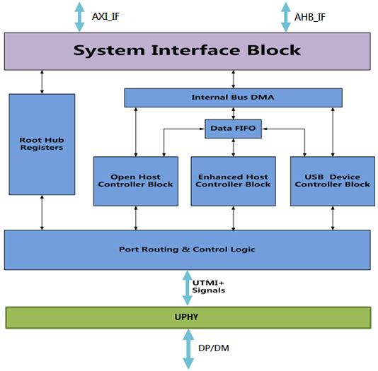
Figure 1314-1 USB Functional Blocks
- AHB_IF: Advanced High-performance Bus (AHB) Interface block, used as AHB bus master data and configure register
- AXI_IF: Advanced Extensible Interface (AXI) block, used for high performance read, write and address access.
- Enhanced Host Controller Block(EHCI): Standard Enhanced Host Controller Interface IP.
- Open Host Controller Block(OHCI): Standard Open Host Controller Interface IP.
- USB Device Controller Block(UDC): SUNPLUS USB Device Controller IP.
- Hub Configure registers(RHREG): Root Hub Configure registers block
- PORT Routing & Control Logic: Generate PHY Control signals (UTMI).
- UPHY: Convert parallel data of UTMI into serial data, and output to the outside of the chip through differential data lines.
...
14.2.1 OHCI Block Diagram
The EHCI has the same structure as OHCI, so below description will focus on OHCI block. Figure 1314-2 shows generic OHCI Block Diagram. 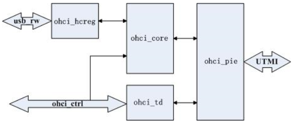
Figure 1314-2 OHCI Block Diagram
- ohci_reg: This is OHCI register control block. Use the AHB master to read/write the OHCI register which generate control signal to OHCI.
- ohci_td: This is OHCI data structure process block. The TD is Transfer Descriptor of OHCI.
- ohci_core: This is OHCI main block, used to R/W ED (Endpoint Descriptor) and TD, and control USB Transfers.
- ohci_pie: This block is used to control USB port state, such as reset、suspend and resume, generate port control signals.
...
14.2.2 USB Device Controller (UDC) Block Diagram
Figure 1314-3 shows a generic UDC Block Diagram.
Figure 1314-3 UDC Block Diagram
- AXI master1:
- Receive the command from USB and issue AXI transition
- It contains 1*audio DMA, 1*video DMA and 3*bulk DMA
- It contains the DMA arbitration mechanism
- AXI master2:
- Including AXI transition control for ISO auto DMA mode
- AHB slave:
- receive the command from system and issue AHB transition
- It contains the configure registers, CPU can write or read these registers by AHB bus
- DMA: DMA logic, issue data transition
- ISO DMA: ISO auto DMA block
- Including ISO IN and ISO OUT DMA control for TRB and Data Read/Write
- Including DMA arbitration mechanism
- SYNC: Sync logic between SYS clock domain and PHY clock domain
- Async FIFO: Sync data between the two clock domain
- Buffer: data buffer
- EPx: EPx (Endpoint x) control logic
- Device IP Link-layer: USB link layer transition logic
- EP5 DMA: ISO IN DMA for Endpoint5
- EP7 DMA: ISO IN DMA for Endpoint7
- EPC DMA: ISO OUT DMA for EndpointC
- DMA ARB: DMA Arbiter for ISO Endpoints
1314.2.3 OTG Transceiver Block Diagram
Figure 1314-4 shows a generic OTG Transceiver Block Diagram.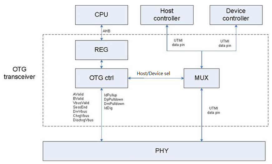
Figure 1314-4 OTG Transceiver Block Diagram
- REG: Receive the command from system and issue AHB transition. It contains the configure registers and CPU can read or write these registers by AHB bus.
- OTG ctrl: Provide flags to deal with OTG functions (SRP/HNP/ADP). It also provides select signal to MUX module.
- MUX: Select UTMI data to host controller or device controller.
...
14.2.4 UPHY Block Diagram
Figure 1314-5 shows a generic UPHY Block Diagram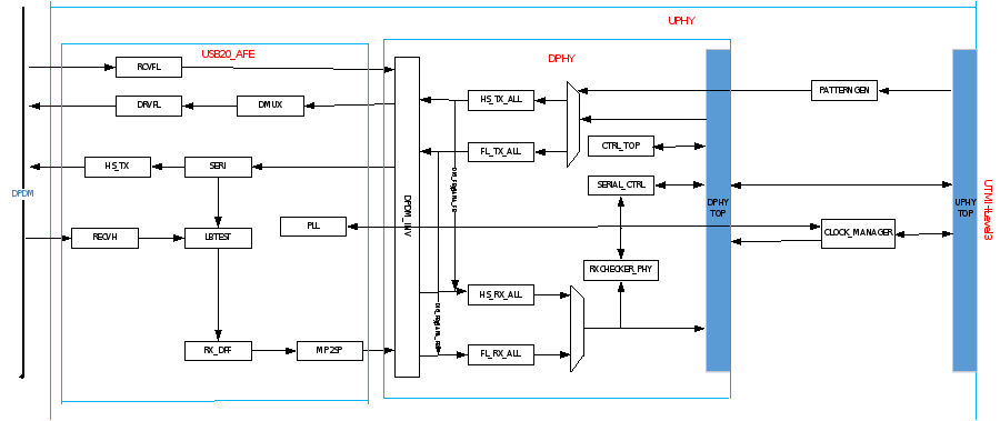
Figure 1314-5 UPHY Block Diagram
- FS_TX_ALL/HS_TX_ALL : Receive signals from the UTMI interface in full-speed, low-speed and high-speed mode, through bit stuffer and encode, then pass the buffer to the APHY
- FS_RX_ALL : Receive data from the APHY in full-speed or low-speed mode. After Decode and bit unstuffing, the data is converted to UTMI and output to Host or Device.
- HS_RX_ALL : In high-speed mode, 20bit data is accepted from the APHY, and the data is separated from the clock according to the CDR, and 5 bit data is sampled. After Decode and bit unstuffing, the data is output from the UTMI interface to Host or Device.
- PATTERNGEN: Generate test-related patterns through I2C or BIST mode
- CTRL_TOP :
- The TX/RX enable signal of HS/FS/LS is generated based on the UTMI signal.
- Output line state signal on UTMI interface
- Control pull-up and pull-down resistors on the DP/DM line
- In HS mode, generate HOST_DISC signal, HOST_DISC=0, device connection, HOST_DISC=1, device disconnected
- SERIAL_CTRL: Write or read register values to UPHY internally via I2C or RGST BUS mode
- CLOCK_MANAGER: Generate L120_CLK and UTMI_CLK. When suspend, generate PLL_OFF to turn off the PLL.
- RXCHECKER_PHY: Check if the data during transmission is correct
...
14.3 USB Host Controller
When insert a USB device, the USB host controller will trigger EHCI/OHCI interrupt to tell software that there is a USB device inserted.
...
14.3.1 OHCI Controller
Figure 1314-6 shows four main areas of a Universal Serial Bus system. These areas are the Client Software/USB Driver, Host Controller Driver (HCD), Host Controller (HC) and USB Device. OHCI specifies the interface between the Host Controller Driver and the Host Controller and the fundamental operation of each.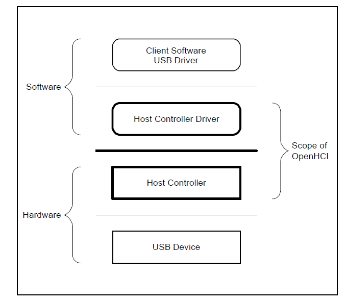
Figure 1314-6 OHCI controller
There are two communication channels between the Host Controller and the Host Controller Driver (Please refer to figure 1314-7). The first channel uses a set of operational registers located on the HC. The Host Controller is the target for all communication on this channel. The operational registers contain control, status, and list pointer registers. Within the operational register set is a pointer to a location in shared memory named the Host Controller Communications Area (HCCA). The HCCA is the second communication channel. The Host Controller is the master for all communication on this channel. The HCCA contains the head pointers to the interrupt Endpoint Descriptor lists, the head pointer to the done queue, and status information associated with start-of-frame processing. 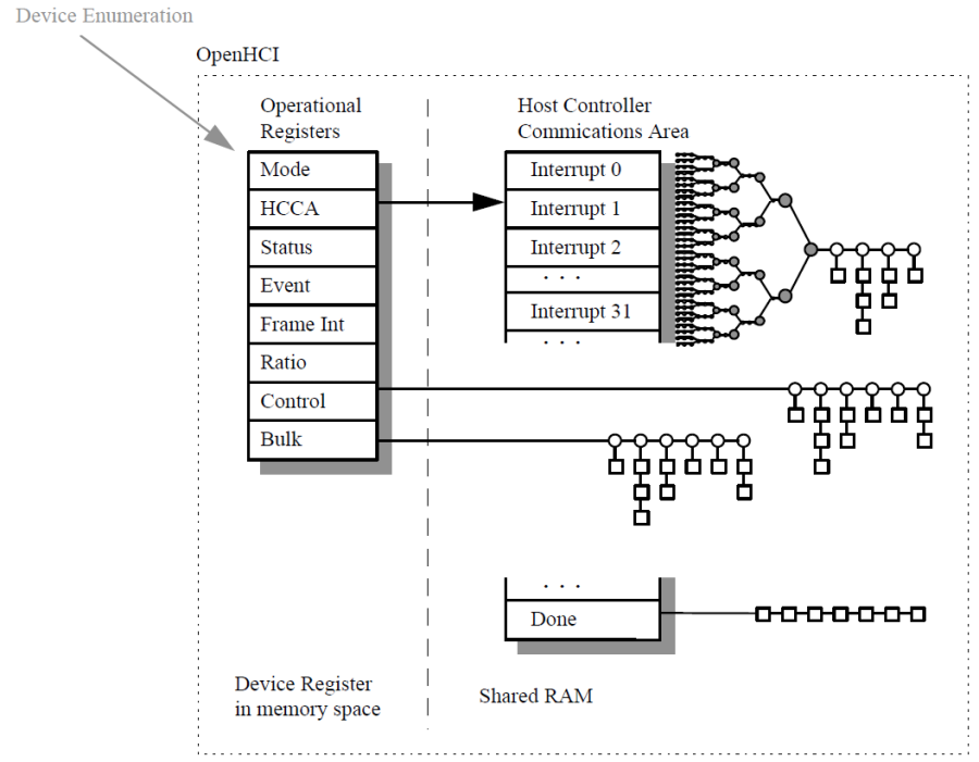
Figure 1314-7 OHCI communication channel
...
14.3.2 EHCI Controller
A USB Host System is composed of a number of hardware and software layers. The Figure 1314-8 illustrates a conceptual block diagram of the building block layers in a host system that work in concert to support USB2.0.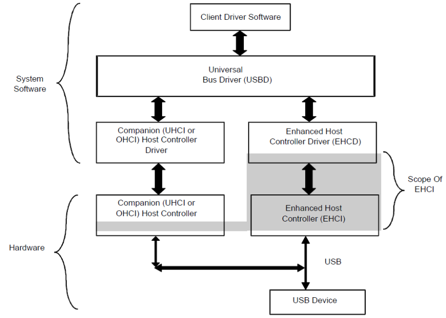
Figure 1314-8 EHCI controller
This architecture allows the USB 2.0 host controller to provide USB functionality as long as there is at least USB 1.1 software support in the resident operating system. Full USB 2.0 functionality is delivered when both USB 1.1 and EHCI software is available in the operating system. The port transceiver routing logic is key to delivering this flexible operating environment. The state of the routing logic initially depends on whether software has configured the EHCI controller. Once the EHCD driver has configured the EHCI controller, it can specifically release the transceiver to the companion host controller port register if the attached device is not a high-speed device. When the operating system does not include support for the EHCI controller, the ports are default-routed to the companion host controllers and existing USB support for Full- and Low-speed devices remains.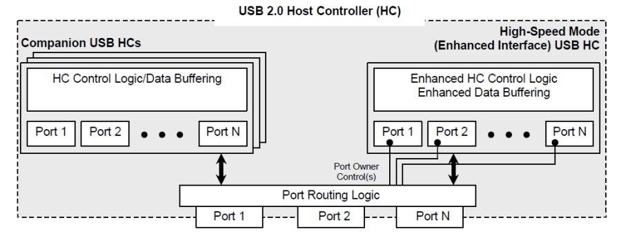
Figure 1314-9 Companion Host Controller
The Companion Host Controller (CHC) may be any USB 1.1 host controller (e.g. OHCI or UHCI). The Companion Host Controllers always manage Full- and Low-speed USB devices connected to the root ports. The CHCs have no knowledge of the high-speed-mode host controller. They can possibly be integrated into a USB 2.0 host controller with no modification.
The EHCI interface defines three interface spaces:
- PCI Configuration Space: If the implementation includes PCI registers, they are used for system component enumeration and PCI power management.
- Register Space: Implementation-specific parameters and capabilities, plus operational control and status registers. This space, normally referred to as I/O space, must be implemented as memory-mapped I/O space.
- Schedule Interface Space: This is typically memory allocated and managed by the EHC Driver for the periodic and asynchronous schedules.
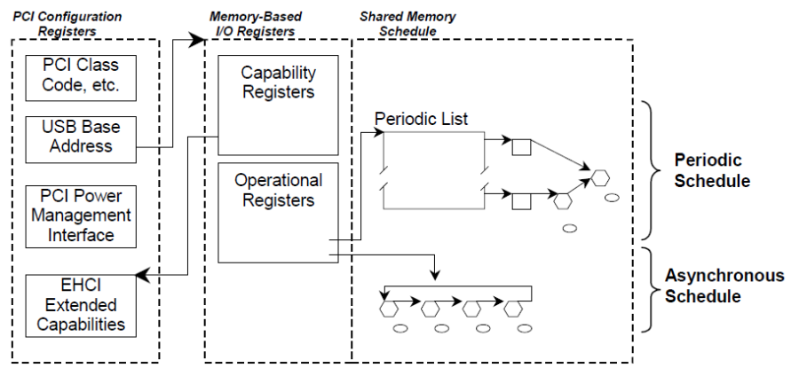
Figure 1314-10 EHCI interface
...
14.3.3 OTG Controller
OTG driver used to control OTG controller work normally. OTG driver mainly maintain a OTG state machine and reflect platform USB state. When OTG is in the different OTG state, OTG driver will control OTG controller to do different things. For example, when OTG state become A-device, OTG driver configure registers to raise VBUS signal and control OTG controller to switch platform to USB host mode. When OTG state become B-device, OTG driver will configure registers to drop VBUS signal and control OTG controller to switch platform to USB device mode to wait host enumerate itself. And so on.
...
14.4 Data Transfer Types
There are four data transfer types defined in USB. Each type is optimized to match the service requirements between the client software and the USB device. The four types are:
...
In OHCI the data transfer types are classified into two categories: periodic and nonperiodic. Periodic transfers are interrupt and isochronous since they are scheduled to run at periodic intervals. Nonperiodic transfers are control and bulk since they are not scheduled to run at any
specific time, but rather on a time-available basis.
...
14.5 Data Structure
...
14.5.1 OHCI Data Structure
The basic building blocks for communication across the interface are the Endpoint Descriptor(ED) and Transfer Descriptor (TD). Each data transfer type has its own linked list of Endpoint Descriptors to be processed. Figure 1314-10, Typical List Structure, is a representation of the data structure relationships.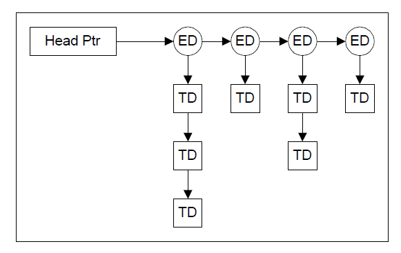
Figure 1314-11 OHCI data structure
Endpoint Descriptors
The Host Controller Driver assigns an Endpoint Descriptor to each endpoint in the system. The Endpoint Descriptor contains the information necessary for the Host Controller to communicate with the endpoint. The fields include the maximum packet size, the endpoint address, the speed of the endpoint, and the direction of data flow. Endpoint Descriptors are linked in a list.
An Endpoint Descriptor (ED) is a 16-byte, memory resident structure that must be aligned to a 16-byte boundary. The Host Controller traverses lists of EDs and if there are TDs linked to an ED, the Host Controller performs the indicated transfer.
Figure 1314-11 shows Endpoint Descriptor Format.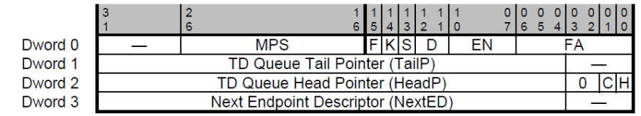
Figure 1314-12 Endpoint Descriptor Format
Notes:
1. Fields containing '—' are not interpreted or modified by the Host Controller and are available for use by the Host Controller Driver for any purpose.
2. Fields containing '0' must be written to 0 by the Host Controller Driver before queued for Host Controller processing. If Host Controller has write access to the field, it will always write the field to 0.
Transfer Descriptors
A queue of Transfer Descriptors is linked to the Endpoint Descriptor for the specific endpoint. The Transfer Descriptor contains the information necessary to describe the data packets to be transferred. The fields include data toggle information, shared memory buffer location and completion status codes. Each Transfer Descriptor contains information that describes one or more data packets. The data buffer for each Transfer Descriptor ranges in size from 0 to 8192 bytes with a maximum of one physical page crossing. Transfer Descriptors are linked in a queue, the first one queued is the first one processed.
A Transfer Descriptor (TD) is a system memory data structure that is used by the Host Controller to define a buffer of data that will be moved to or from an endpoint. TDs come in two types: general and isochronous. The General TD is used for Interrupt, Control, and Bulk Endpoints and an Isochronous TD is used to deal with the unique requirements of isochronous transfers. Two TD types are supported because the nature of isochronous transfers does not lend itself to the standard DMA buffer format and the packetizing of the buffer required for isochronous transfers is too restrictive for general transfer types.
General Transfer Descriptor
Transfers for control, bulk, and interrupt all use the same format for their Transfer Descriptor (TD). This General TD is a 16-byte, host memory structure that must be aligned to a 16-byte boundary.
Figure 1314-12 shows General Transfer Descriptor Format.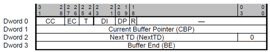
Figure 1314-13 General Transfer Descriptor Format
Isochronous Transfer Descriptor
An Isochronous TD is used exclusively for isochronous endpoints. All TDs linked to an ED with F = 1 must use this format. This 32-byte structure must be aligned to a 32-byte boundary in system memory.
Figure 1314-13 shows General Transfer Descriptor Format.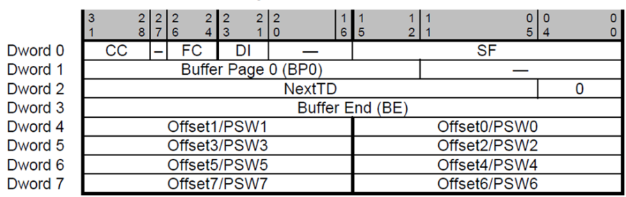
Figure 1314-14 Isochronous Transfer Descriptor Format
...
14.5.2 EHCI Data Structure
The data structure definitions in this chapter support a 32-bit memory buffer address space. The interface consists of a Periodic Schedule, Periodic Frame List, Asynchronous Schedule, Isochronous Transaction Descriptors, Split-transaction Isochronous Transfer Descriptors, Queue Heads and Queue Element Transfer Descriptors.
Periodic Frame List
This schedule is for all periodic transfers (isochronous and interrupt). The periodic schedule is referenced from the operational registers space using the PeriodicListBase address register and the FRINDEX register. The periodic schedule is based on an array of pointers called the Periodic Frame List. The PeriodicListBase address register is combined with the FRINDEX register to produce a memory pointer into the frame list. The Periodic Frame List implements a sliding window of work over time.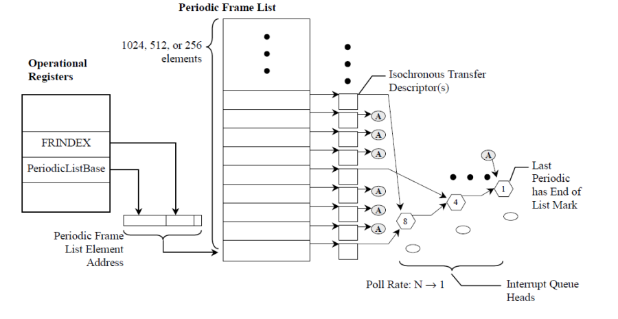
Figure 1314-15 Periodic Frame List
Asynchronous List Queue Head Pointer
The Asynchronous Transfer List (based at the AsyncListAddr register), is where all the control and bulk transfers are managed. Host controllers use this list only when it reaches the end of the periodic list, the periodic list is disabled, or the periodic list is empty.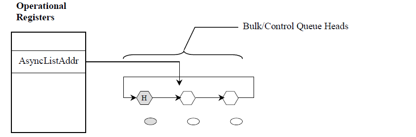
Figure 1314-16 Asynchronous Transfer List
...
14.6 UTM Interface Timing Diagram
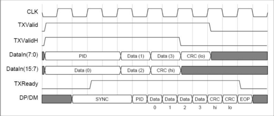
Figure 1314-17 TX odd byte data
Figure 1314-18 TX even byte data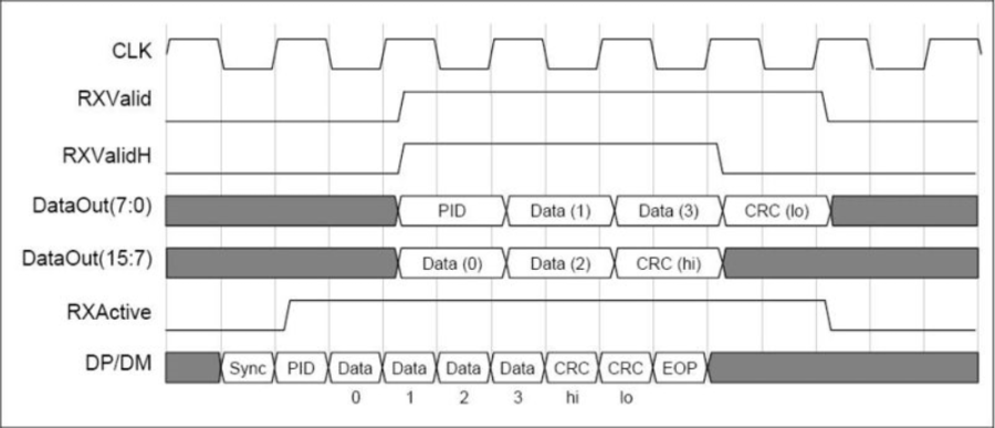
Figure 1314-19 RX odd byte data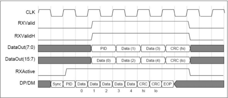
Figure 1314-20 RX even byte data
...
14.7 OHCI USB States
The Host Controller has four USB states visible to the Host Controller Driver via the Operational Registers: USBOPERATIONAL, USBRESET, USBSUSPEND, and USBRESUME. These states define the Host Controller responsibilities relating to USB signaling and bus states.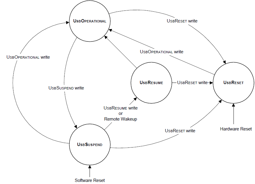
Figure 1314-21 USB states
...
14.7.1 USBOPERATIONAL
When in the USBOPERATIONAL state, the Host Controller may process lists and will generate SOF Tokens. The USBOPERATIONAL state may be entered from the USBRESUME or USBRESET states. It may be exited to the USBRESET or USBSUSPEND states. When transitioning from USBRESET or USBRESUME to USBOPERATIONAL, the Host Controller is responsible for terminating the USB reset or resume signaling as defined in the USB Specification prior to sending a token.
...
14.7.2 USBRESET
When in the USBRESET state, the Host Controller forces reset signaling on the bus. The Host Controller's list processing and SOF Token generation are disabled while in USBRESET. The USBRESET state can be entered from any state at any time. The Host Controller defaults to the USBRESET state following a hardware reset. The Host Controller Driver is responsible for satisfying USB Reset signaling timing defined by the USB Specification.
...
14.7.3 USBSUSPEND
The USBSUSPEND state defines the USB Suspend state. The Host Controller's list processing and SOF Token generation are disabled. However, the Host Controller's remote wakeup logic must monitor USB wakeup activity. USBSUSPEND is entered following a software reset or from the USBOPERATIONAL state on command from the Host Controller Driver. While in USBSUSPEND, the Host Controller may force
a transition to the USBRESUME state due to a remote wakeup condition. This transition may conflict with the Host Controller Driver initiating a transition to the USBRESET state. If this situation occurs, the HCD-initiated transition to USBRESET has priority. The Host Controller Driver must wait 5 ms after transitioning to USBSUSPEND before transitioning to the USBRESUME state. Likewise, the Root Hub must wait 5 ms after the Host Controller enters USBSUSPEND before generating a local wakeup event and forcing a transition to USBRESUME. Following a software reset, the Host Controller Driver may cause a transition to USBOPERATIONAL if the transition occurs no more than 1 ms from the transition into USBSUSPEND. If the 1-ms period is violated, it is possible that devices on the bus will go into Suspend.
...
14.7.4 USBRESUME
When in the USBRESUME state, the Host Controller forces resume signaling on the bus. While in USBRESUME, the Root Hub is responsible for propagating the USB Resume signal to downstream ports as specified in the USB Specification. The Host Controller's list processing and SOF Token generation are disabled while in USBRESUME. USBRESUME is only entered from USBSUSPEND. The transition to USBRESUME can be initiated by the Host Controller Driver or by a USB remote wakeup signaled by the Root Hub. The Host
Controller is responsible for resolving state transition conflicts between the hardware wakeup and Host Controller Driver initiated state transitions. Legal state transitions from USBRESUME are to USBRESET and to USBOPERATIONAL. The Host Controller Driver is responsible for USB Resume signal timing as defined by the USB Specification.
...
14.8 USB OPERATION
...
14.8.1 OHCI Initialization
Initialize the open host controller, software should perform the following steps:
...
Note: Due to some devices on the USB that may take a long time to reset, it is desirable that the Host Controller Driver startup process not transition to the USBRESET state if possible.
...
14.8.2 EHCI Initialization
In order to initialize the enhanced host controller, software should perform the following steps:
- Set software reset in Group2.8 UHE_USBCMD register bit[1]=1.
- Program the Group2.12 UHE_CTRLDESSEGMENT register with 4-Gigabyte segment where all of the interface data structures are allocated.
- Write the appropriate value to the Group2.10 UHE_USBINTR register to enable the appropriate interrupts.
- Write the base address of the Periodic Frame List to the Group2.13 UHE_PERIODICLISTBASE register. Write the base address of the Asynchronous Frame List to the Group2.14 UHE_ASYNCLISTBASE register.
- Enable Periodic schedule in Gruop2.8 UHE_USBCMD register bit4, enable Asynchronous schedule in Gruop2.8 UHE_USBCMD register bit5.
- Write the Group2.8 UHE_USBCMD register to set the desired interrupt threshold, frame list size (if applicable).
- Write 1 to bit0 of Group2.24 UHE_CONFIGFLAG register to route all ports to the EHCI controller.
- Wait device connect by check Group2.25 UHE_PORTSC register bit0=1.
- Issue port reset by set Group2.25 UHE_PORTSC register bit8=1.
- Turn the host controller ON via setting the Run/Stop bit in Gruop2.8 UHE_USBCMD register bit0.
...
14.8.3 OTG Initialization
- Select work mode in Group8.0 MODE_SELECT register bit[1:0]. Default as 0 with OTG2.0.
- Confirm work role by read Group8.0 MODE_SELECT register bit[1:0] after "ID_CHANGE_IF" interrupt is assert. The ID_CHANGE_IF flag is in Group8.3 OTG_ST register bit1.
- Depend on work mode, set initial of OTG CTRL in Group8.1 OTG_DEVICE_CTRL register. Set SRP/ADP_SUPPORT in Group8.0 MODE_SELECT bit2 and bit3
- Set SRP/HNP/ADP related timers in Group8.4~8.29 registers.
...
14.9 Pattern of come to USB2.0
Define the line state J, K, SE0 of USB, that is, D+, D-, as shown in the following table.
...
USB 2.0 is made under the existing architecture that does not destroy USB1.1. Unless host and device are both 2.0, they are all transmitted with 1.1. The method of recognition is chirp, which is described as follows. The yellow line is D+ and the blue line is D-. The timing is as follows: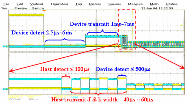
Figure 1314-22 USB2.0 chirp pattern
- D+ pull up to 3.3V after device plug in
- Host drive bus reset (se0, both D+,D- = 0)
- Device chirp K 1ms-7ms. (D- = 800mV)
- Host chirp KJKJKJ sequence pattern
- Device recognizes 6 groups of kj and enters USB2.0 mode, turn on 45 Ohm pull down to GND at the same time, it make 800mV level become 400mV.
...
14.10 USB Interrupts
...
14.10.1 OHCI Interrupts
OHCI interrupt is from OHCI block with level signals. The detail interrupt information refer to the USBC0 Group1.3 bit[6:0] UHO_HcInterruptStatus Register. The enable register is USBC0 Group1.4 bit[6:0] UHO_HcInterruptEnable. Figure 1314-23 shows the OHCI interrupt tree.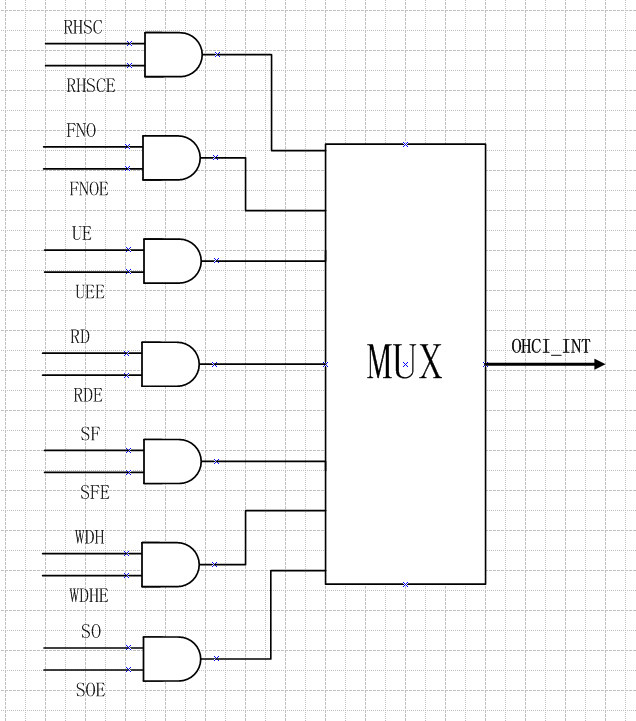
Figure 1314-23 OHCI interrupt tree
- RHSC: Root Hub content change status bit
- FNO: Frame number overflow status bit
- UE: Un-recoverable error
- RD: Resume signaling detected status bit
- SF: Each start of a frame status bit
- WDH: HC has written HcDoneHead to HccaDoneHead status bit
- SO: USB schedule for the current Frame overruns status bit
...
14.10.2 EHCI Interrupts
EHCI interrupt is from EHCI block with level signals. The detail interrupt information refer to the USBC0 Group2.9 bit[5:0] UHE_USBSTS register. The enable register is USBC0 Group2.10 bit[5:0] UHE_USBINTR. Figure 1314-24 shows the EHCI interrupt tree.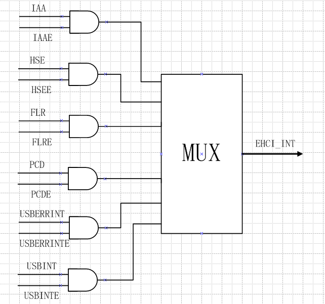
Figure 1314-24 EHCI interrupt tree
- IAA: Indicates the assertion of Async Advance interrupt
- HSE: Host system error
- FLR: Indicate the Frame List Index rolls over from its maximum value to zero
- PCD: Indicate any port of the port owner bit is set to zero or from zero to a one
- USBERRINT: Indicate completion of a USB transaction results in an error condition
- USBINT: Indicate the completion of a USB transaction
...
14.10.3 OTG Interrupts
The detail OTG interrupt information refer to the USBC0 Group8.3 bit[9:0] OTG_ST register. The enable register is USBC0 Group8.2 bit[9:0] OTG_INT_EN. Figure 1314-25 shows the OTG interrupt tree.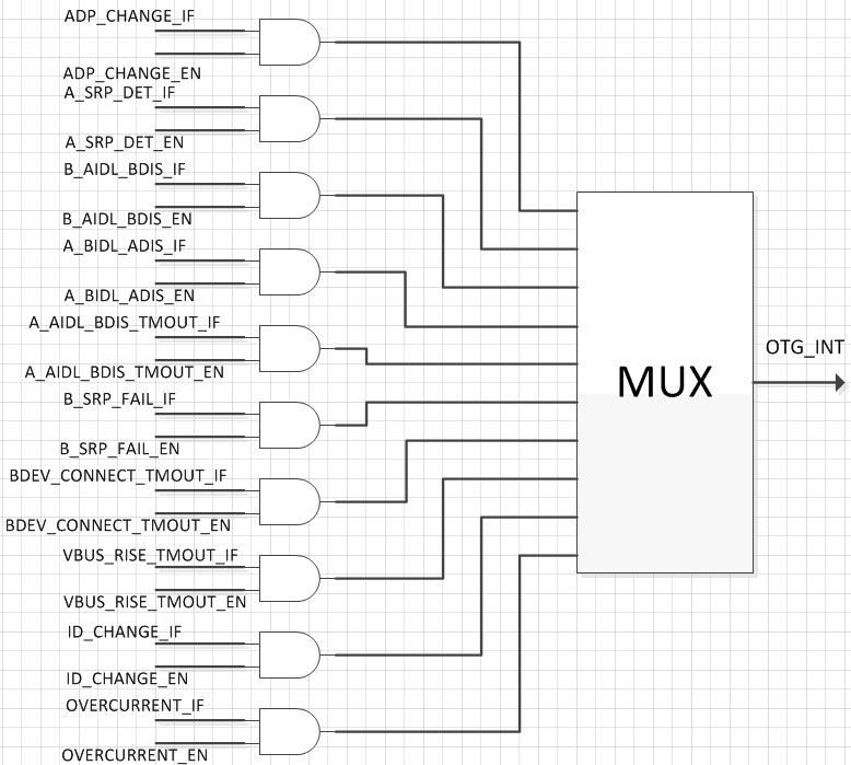
Figure 1314-25 OTG interrupt tree
- ADP_CHANGE_IF: Indicate the ADP changed
- A_SRP_DET_IF: Indicate A-device(Host side) have detected SRP
- B_AIDL_BDIS_IF: Indicate B-device(Device side) disconnects to A-device(Host side) to start HNP
- A_BIDL_ADIS_IF: Indicate A-device(Host side) disconnects to B-device(Device side) to start HNP
- A_AIDL_BDIS_TMOUT_IF: Waiting for a disconnect timeout when HNP
- B_SRP_FAIL_IF: B-device SRP fail
- BDEV_CONNECT_TMOUT_IF: A-device waits B-device connect timeout
- VBUS_RISE_TMOUT_IF: A-device waits vbus valid timeout
- ID_CHANGE_IF: ID pin has changed
- OVERCURRENT_IF: An attached B-device draws more current
...
14.11 Registers Map
...
14.11.1 Registers Memory Map
Memory Map Start Address | Data Width | Group No. | Module |
|---|---|---|---|
0x9C004A80 | 32 | 149 | UPHY0 (USB PHY 0) |
0x9C004B00 | 32 | 150 | UPHY1 (USB PHY1) |
Table 1314-1 USB PHY registers group list of RGST table
Both USB PHY registers have the same offset in corresponding register group. Only USB PHY0 (UPHY0) registers are described in following register description, for USB PHY1 please refer to UPHY0 description for more detail.
Memory Map Start Address | Data Width | Group No. | Module |
|---|---|---|---|
0x9C102000 | 32 | USBC0 Group 0 | USB0 HOST |
0x9C102080 | 32 | USBC0 Group 1 | USB0 OHCI |
0x9C102100 | 32 | USBC0 Group 2 | USB0 EHCI |
0x9C102400 | 32 | USBC0 Group 8 | USB0 OTG |
0x9C102800 | 32 | USBC0 Group 16 | USB0 DMA |
0x9C102880 | 32 | USBC0 Group 17 | USB0 INTERRUPT |
0x9C102900 | 32 | USBC0 Group 18 | USB0 EP0~4 |
0x9C102980 | 32 | USBC0 Group 19 | USB0 EP5/6/7 |
0x9C102A00 | 32 | USBC0 Group 20 | USB0 EP8/9/A/B |
0x9C102A80 | 32 | USBC0 Group 21 | USB0 EPC/D |
0x9C102B00 | 32 | USBC0 Group 22 | USB0 Phyclk Domain Interrupt |
0x9C102B80 | 32 | USBC0 Group 23 | USB0 Bulk Out FIFO |
0x9C103000 | 32 | USBC1 Group 0 | USB1 HOST |
0x9C103080 | 32 | USBC1 Group 1 | USB1 OHCI |
0x9C103100 | 32 | USBC1 Group 2 | USB1 EHCI |
0x9C103400 | 32 | USBC1 Group 8 | USB1 OTG |
0x9C103800 | 32 | USBC1 Group 16 | USB1 DMA |
0x9C103880 | 32 | USBC1 Group 17 | USB1 INTERRUPT |
0x9C103900 | 32 | USBC1 Group 18 | USB1 EP0~4 |
0x9C103980 | 32 | USBC1 Group 19 | USB1 EP5/6/7 |
0x9C103A00 | 32 | USBC1 Group 20 | USB1 EP8/9/A/B |
0x9C103A80 | 32 | USBC1 Group 21 | USB1 EPC/D |
0x9C103B00 | 32 | USBC1 Group 22 | USB1 Phyclk Domain Interrupt |
0x9C103B80 | 32 | USBC1 Group 23 | USB1 Bulk Out FIFO |
Table 1314-2 USB control registers group list of AMBA table
Only USB0 relative register group will be described in register description, for USB1, please refer to USB0 corresponding group description for more detail
...
14.11.2 Registers Description
RGST Table Group 149 UPHY0
149.0 CONFIG0 (cfg0)
Address: 0x9C004A80
Reset: 0x0000 0080
...
| Field Name | Bit | Access | Description |
| Reserved | 31:8 | RO | RESERVED |
Reserved | 7 | RW | RESERVED |
Reserved | 6 | RW | RESERVED |
NA | 5:0 | RW | NA |
J AC2 0 B | 5:3 | RW | OTG Discharge Current Option. 0x0: 5uA 0x1: 10uA 0x2: 15uA 0x3: 20uA 0x4: 30uA (default) 0x5: 40uA 0x6: 50uA 0x7: 60uA |
J AC2 0 | 2:0 | RW | OTG Charge Current Option. 0x0: 5uA 0x1: 10uA 0x2: 15uA 0x3: 20uA 0x4: 30uA (default) 0x5: 40uA 0x6: 50uA 0x7: 60uA |
...