14. Universal Serial Bus (USB)
- edwin.chiu (Unlicensed)
- Michael Su (Unlicensed)
14.1 Introduction
The USB is specified to be an industry-standard extension to the PC architecture. It provides an USB compliant connection between the host PC and the function implemented by the microcontroller. It also supports USB-OTG (On-The-Go) function to connect with peripheral USB devices. Data transfer between the host PC and the system memory occurs through a dedicated packet buffer memory accessed directly by the USB peripheral. The size of this dedicated buffer memory must be according to the number of endpoints used and maximum packet size. The dedicated memory is sized to 512bytes and up to 16 mono-directional endpoints can be used. This USB supports 4 kind endpoint transactions, they are Control, Bulk, Interrupt and Isochronous transfer mode.
A USB system is described by three definitional areas, USB PHY (UPHY) , USB Controller System (USBC) and On-The-Go (OTG) Controller. Where USB Controller system includes two major parts: USB host controller(UHC) and USB device controller(UDC). The USB transfer signals and power over a four-wire cable, the signaling occurs over wires on each point-to-point segment.
The USB HOST IP (UHC) is a USB2.0 Host Controller, Support both Enhanced Host Controller Interface (EHCI) and Open Host Controller Interface (OHCI), 32bit AHB/AXI configure bus, 64bit AXI data bus. The USB DEVICE IP (UDC) is a standard USB Device Controller which supports USB2.0 High Speed and Full speed, AXI Master bus, AXI Master1 bus (used for ISO auto DMA), AHB slave bus and UTMI (USB2.0 Transceiver Macrocell Interface) interface. The USB PHY module supports working in Host or Device mode and can dynamic switch.
The USB control registers located in the memory map address range of 9c102000h~9c103fffh. The USB PHY control registers located in the 9c004a80h~9c004b7fh. SP7021 totally supports two USB2.0 modules, the features list as below.
- UTMI+ level3 compatible with OTG
- 27MHz crystal input to support Battery Charger and sync signals
- Integrated Phase-Locked Loop (PLL) oscillator generate 120M CLK to DPHY
- Supports various power down modes include Operating, Partial and Suspend modes
- Supports high-speed (HS, 480 Mbps), full-speed (FS, 12Mbps) and low-speed (LS, 1.5Mbps) data transfer rates
- OTG supports Attach Detection Protocol (ADP), Session Request Protocol (SRP) and Host Negotiation Protocol (HNP)
- Support boot from each USB port
- Support USB video class (UVC)
14.2 Function Diagram
A generalized function diagram of USB is shown in Figure 14-1.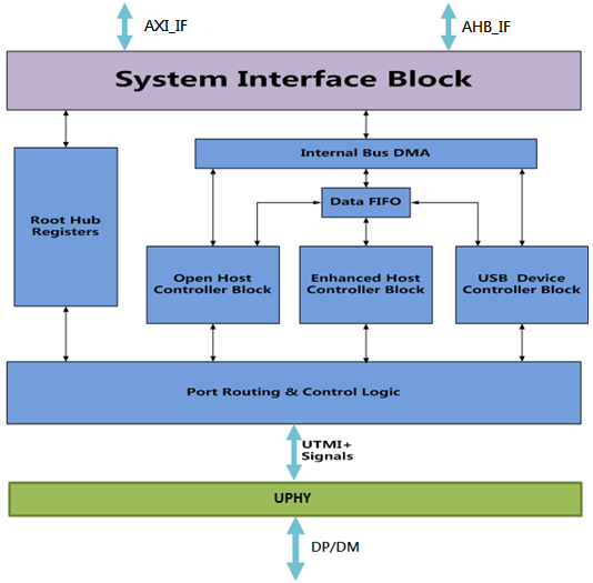
Figure 14-1 USB Functional Blocks
- AHB_IF: Advanced High-performance Bus (AHB) Interface block, used as AHB bus master data and configure register
- AXI_IF: Advanced Extensible Interface (AXI) block, used for high performance read, write and address access.
- Enhanced Host Controller Block(EHCI): Standard Enhanced Host Controller Interface IP.
- Open Host Controller Block(OHCI): Standard Open Host Controller Interface IP.
- USB Device Controller Block(UDC): SUNPLUS USB Device Controller IP.
- Hub Configure registers(RHREG): Root Hub Configure registers block
- PORT Routing & Control Logic: Generate PHY Control signals (UTMI).
- UPHY: Convert parallel data of UTMI into serial data, and output to the outside of the chip through differential data lines.
14.2.1 OHCI Block Diagram
The EHCI has the same structure as OHCI, so below description will focus on OHCI block. Figure 14-2 shows generic OHCI Block Diagram. 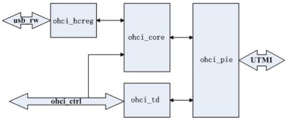
Figure 14-2 OHCI Block Diagram
- ohci_reg: This is OHCI register control block. Use the AHB master to read/write the OHCI register which generate control signal to OHCI.
- ohci_td: This is OHCI data structure process block. The TD is Transfer Descriptor of OHCI.
- ohci_core: This is OHCI main block, used to R/W ED (Endpoint Descriptor) and TD, and control USB Transfers.
- ohci_pie: This block is used to control USB port state, such as reset、suspend and resume, generate port control signals.
14.2.2 USB Device Controller (UDC) Block Diagram
Figure 14-3 shows a generic UDC Block Diagram.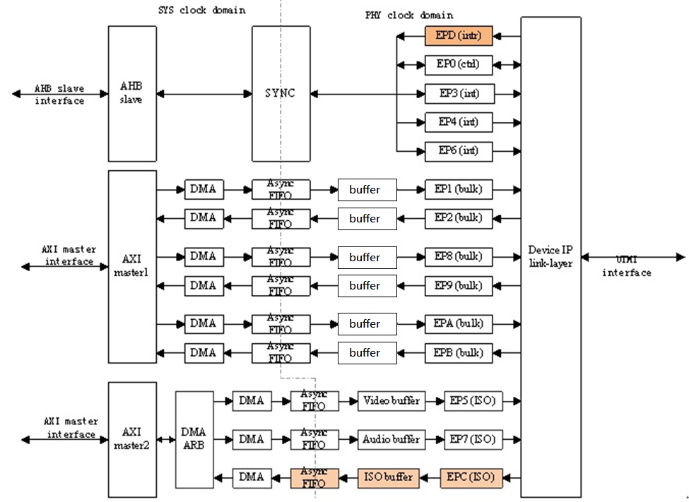
Figure 14-3 UDC Block Diagram
- AXI master1:
- Receive the command from USB and issue AXI transition
- It contains 1*audio DMA, 1*video DMA and 3*bulk DMA
- It contains the DMA arbitration mechanism
- AXI master2:
- Including AXI transition control for ISO auto DMA mode
- AHB slave:
- receive the command from system and issue AHB transition
- It contains the configure registers, CPU can write or read these registers by AHB bus
- DMA: DMA logic, issue data transition
- ISO DMA: ISO auto DMA block
- Including ISO IN and ISO OUT DMA control for TRB and Data Read/Write
- Including DMA arbitration mechanism
- SYNC: Sync logic between SYS clock domain and PHY clock domain
- Async FIFO: Sync data between the two clock domain
- Buffer: data buffer
- EPx: EPx (Endpoint x) control logic
- Device IP Link-layer: USB link layer transition logic
- EP5 DMA: ISO IN DMA for Endpoint5
- EP7 DMA: ISO IN DMA for Endpoint7
- EPC DMA: ISO OUT DMA for EndpointC
- DMA ARB: DMA Arbiter for ISO Endpoints
14.2.3 OTG Transceiver Block Diagram
Figure 14-4 shows a generic OTG Transceiver Block Diagram.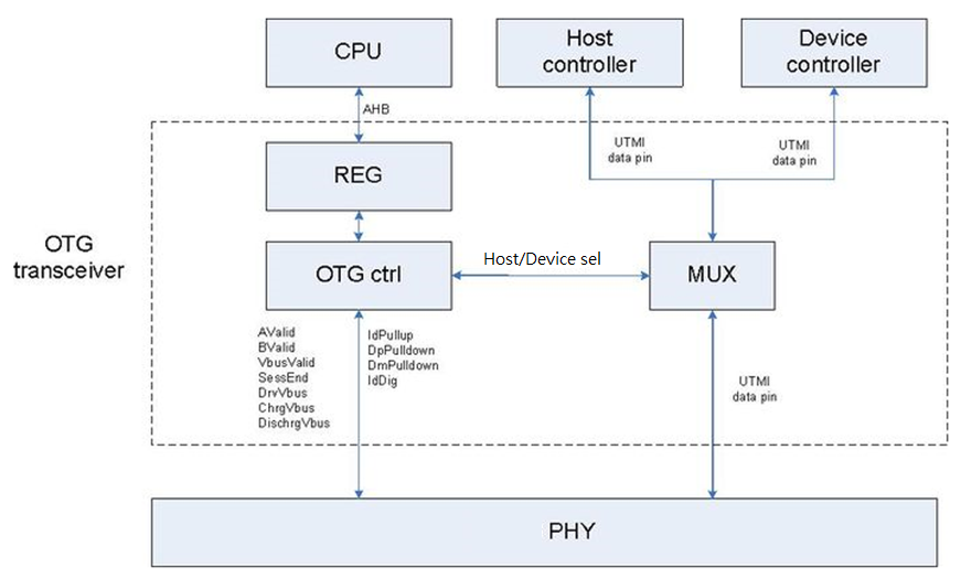
Figure 14-4 OTG Transceiver Block Diagram
- REG: Receive the command from system and issue AHB transition. It contains the configure registers and CPU can read or write these registers by AHB bus.
- OTG ctrl: Provide flags to deal with OTG functions (SRP/HNP/ADP). It also provides select signal to MUX module.
- MUX: Select UTMI data to host controller or device controller.
14.2.4 UPHY Block Diagram
Figure 14-5 shows a generic UPHY Block Diagram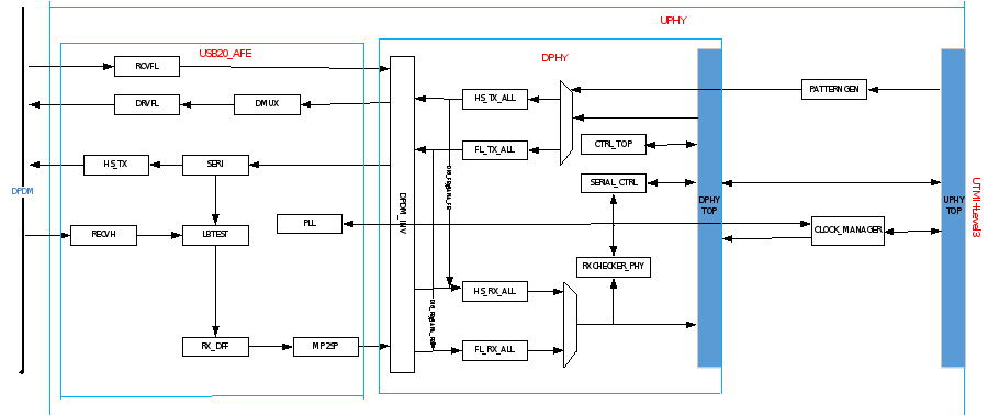
Figure 14-5 UPHY Block Diagram
- FS_TX_ALL/HS_TX_ALL : Receive signals from the UTMI interface in full-speed, low-speed and high-speed mode, through bit stuffer and encode, then pass the buffer to the APHY
- FS_RX_ALL : Receive data from the APHY in full-speed or low-speed mode. After Decode and bit unstuffing, the data is converted to UTMI and output to Host or Device.
- HS_RX_ALL : In high-speed mode, 20bit data is accepted from the APHY, and the data is separated from the clock according to the CDR, and 5 bit data is sampled. After Decode and bit unstuffing, the data is output from the UTMI interface to Host or Device.
- PATTERNGEN: Generate test-related patterns through I2C or BIST mode
- CTRL_TOP :
- The TX/RX enable signal of HS/FS/LS is generated based on the UTMI signal.
- Output line state signal on UTMI interface
- Control pull-up and pull-down resistors on the DP/DM line
- In HS mode, generate HOST_DISC signal, HOST_DISC=0, device connection, HOST_DISC=1, device disconnected
- SERIAL_CTRL: Write or read register values to UPHY internally via I2C or RGST BUS mode
- CLOCK_MANAGER: Generate L120_CLK and UTMI_CLK. When suspend, generate PLL_OFF to turn off the PLL.
- RXCHECKER_PHY: Check if the data during transmission is correct
14.3 USB Host Controller
When insert a USB device, the USB host controller will trigger EHCI/OHCI interrupt to tell software that there is a USB device inserted.
14.3.1 OHCI Controller
Figure 14-6 shows four main areas of a Universal Serial Bus system. These areas are the Client Software/USB Driver, Host Controller Driver (HCD), Host Controller (HC) and USB Device. OHCI specifies the interface between the Host Controller Driver and the Host Controller and the fundamental operation of each.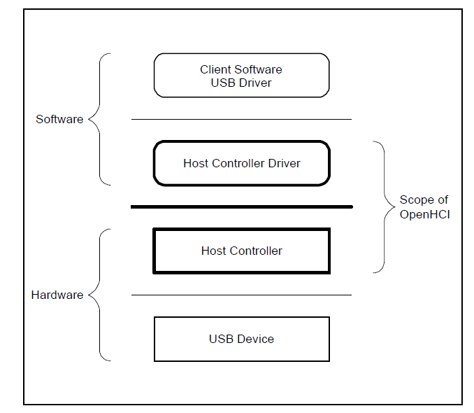
Figure 14-6 OHCI controller
There are two communication channels between the Host Controller and the Host Controller Driver (Please refer to figure 14-7). The first channel uses a set of operational registers located on the HC. The Host Controller is the target for all communication on this channel. The operational registers contain control, status, and list pointer registers. Within the operational register set is a pointer to a location in shared memory named the Host Controller Communications Area (HCCA). The HCCA is the second communication channel. The Host Controller is the master for all communication on this channel. The HCCA contains the head pointers to the interrupt Endpoint Descriptor lists, the head pointer to the done queue, and status information associated with start-of-frame processing. 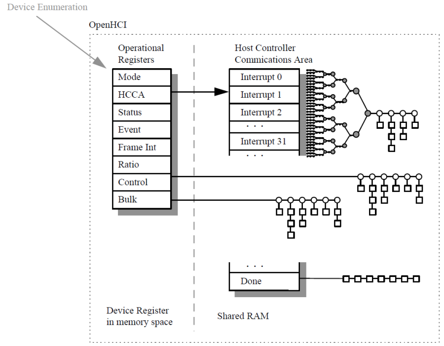
Figure 14-7 OHCI communication channel
14.3.2 EHCI Controller
A USB Host System is composed of a number of hardware and software layers. The Figure 14-8 illustrates a conceptual block diagram of the building block layers in a host system that work in concert to support USB2.0.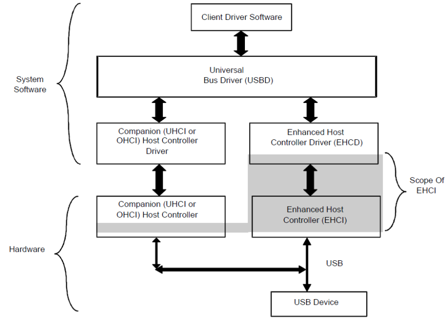
Figure 14-8 EHCI controller
This architecture allows the USB 2.0 host controller to provide USB functionality as long as there is at least USB 1.1 software support in the resident operating system. Full USB 2.0 functionality is delivered when both USB 1.1 and EHCI software is available in the operating system. The port transceiver routing logic is key to delivering this flexible operating environment. The state of the routing logic initially depends on whether software has configured the EHCI controller. Once the EHCD driver has configured the EHCI controller, it can specifically release the transceiver to the companion host controller port register if the attached device is not a high-speed device. When the operating system does not include support for the EHCI controller, the ports are default-routed to the companion host controllers and existing USB support for Full- and Low-speed devices remains.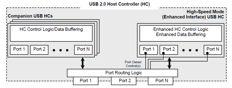
Figure 14-9 Companion Host Controller
The Companion Host Controller (CHC) may be any USB 1.1 host controller (e.g. OHCI or UHCI). The Companion Host Controllers always manage Full- and Low-speed USB devices connected to the root ports. The CHCs have no knowledge of the high-speed-mode host controller. They can possibly be integrated into a USB 2.0 host controller with no modification.
The EHCI interface defines three interface spaces:
- PCI Configuration Space: If the implementation includes PCI registers, they are used for system component enumeration and PCI power management.
- Register Space: Implementation-specific parameters and capabilities, plus operational control and status registers. This space, normally referred to as I/O space, must be implemented as memory-mapped I/O space.
- Schedule Interface Space: This is typically memory allocated and managed by the EHC Driver for the periodic and asynchronous schedules.
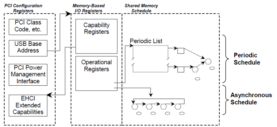
Figure 14-10 EHCI interface
14.3.3 OTG Controller
OTG driver used to control OTG controller work normally. OTG driver mainly maintain a OTG state machine and reflect platform USB state. When OTG is in the different OTG state, OTG driver will control OTG controller to do different things. For example, when OTG state become A-device, OTG driver configure registers to raise VBUS signal and control OTG controller to switch platform to USB host mode. When OTG state become B-device, OTG driver will configure registers to drop VBUS signal and control OTG controller to switch platform to USB device mode to wait host enumerate itself. And so on.
14.4 Data Transfer Types
There are four data transfer types defined in USB. Each type is optimized to match the service requirements between the client software and the USB device. The four types are:
- Control Transfers: Nonperiodic data transfers used to communicate configuration/command/status type information between client software and the USB device. It must be through Endpoint 0, and there can only be one device, and it must be supported. The maximum data size that can be transmitted at one time is 64 bytes and is bidirectional. Basically, when a USB device is plugged into the computer, the computer will ask for some information through Endpoint 0. According to the USB 2.0 specification, Host must reserve 10% of the bandwidth for Control transmission.
- Bulk Transfers: Nonperiodic data transfers used to communicate large amounts of information between client software and the USB device. The maximum size of data that can be transmitted at one time is 512 bytes (HS). It does not guarantee the bandwidth, it is usually HOST that the BUS has a bandwidth to choose to transmit Bulk data. In contrast, if the bandwidth is very idle, the amount of data that can be transmitted per second is large.
- Interrupt Transfers: Small data transfers used to communicate information from the USB device to the client software. The Host Controller Driver polls the USB device by issuing tokens to the device at a periodic interval sufficient for the requirements of the device. The maximum data size that can be transmitted at one time is 1024 bytes (HS), and it is transmitted periodically. The device side needs to declare how long this period is. In HS, it is in micro-second. It requires HOST to guarantee the bandwidth. If HOST cannot meet the bandwidth requirements of this device, HOST can refuse to start the device.
- Isochronous Transfers: Periodic data transfers with a constant data rate. Data transfers are correlated in time between the sender and receiver. It is very similar to Interrupt transmission, but it has no mechanism for error retransmission. All above three mode have a mechanism of error retransmission, and this mechanism is based on the premise that each transmission will have an ACK packet. Isochronous transmission does not require ACK packets, so it naturally can't detect errors.
In OHCI the data transfer types are classified into two categories: periodic and nonperiodic. Periodic transfers are interrupt and isochronous since they are scheduled to run at periodic intervals. Nonperiodic transfers are control and bulk since they are not scheduled to run at any
specific time, but rather on a time-available basis.
14.5 Data Structure
14.5.1 OHCI Data Structure
The basic building blocks for communication across the interface are the Endpoint Descriptor(ED) and Transfer Descriptor (TD). Each data transfer type has its own linked list of Endpoint Descriptors to be processed. Figure 14-10, Typical List Structure, is a representation of the data structure relationships.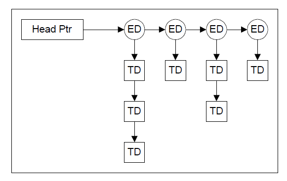
Figure 14-11 OHCI data structure
Endpoint Descriptors
The Host Controller Driver assigns an Endpoint Descriptor to each endpoint in the system. The Endpoint Descriptor contains the information necessary for the Host Controller to communicate with the endpoint. The fields include the maximum packet size, the endpoint address, the speed of the endpoint, and the direction of data flow. Endpoint Descriptors are linked in a list.
An Endpoint Descriptor (ED) is a 16-byte, memory resident structure that must be aligned to a 16-byte boundary. The Host Controller traverses lists of EDs and if there are TDs linked to an ED, the Host Controller performs the indicated transfer.
Figure 14-11 shows Endpoint Descriptor Format.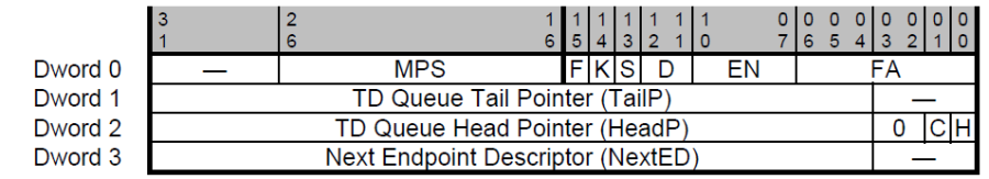
Figure 14-12 Endpoint Descriptor Format
Notes:
1. Fields containing '—' are not interpreted or modified by the Host Controller and are available for use by the Host Controller Driver for any purpose.
2. Fields containing '0' must be written to 0 by the Host Controller Driver before queued for Host Controller processing. If Host Controller has write access to the field, it will always write the field to 0.
Transfer Descriptors
A queue of Transfer Descriptors is linked to the Endpoint Descriptor for the specific endpoint. The Transfer Descriptor contains the information necessary to describe the data packets to be transferred. The fields include data toggle information, shared memory buffer location and completion status codes. Each Transfer Descriptor contains information that describes one or more data packets. The data buffer for each Transfer Descriptor ranges in size from 0 to 8192 bytes with a maximum of one physical page crossing. Transfer Descriptors are linked in a queue, the first one queued is the first one processed.
A Transfer Descriptor (TD) is a system memory data structure that is used by the Host Controller to define a buffer of data that will be moved to or from an endpoint. TDs come in two types: general and isochronous. The General TD is used for Interrupt, Control, and Bulk Endpoints and an Isochronous TD is used to deal with the unique requirements of isochronous transfers. Two TD types are supported because the nature of isochronous transfers does not lend itself to the standard DMA buffer format and the packetizing of the buffer required for isochronous transfers is too restrictive for general transfer types.
General Transfer Descriptor
Transfers for control, bulk, and interrupt all use the same format for their Transfer Descriptor (TD). This General TD is a 16-byte, host memory structure that must be aligned to a 16-byte boundary.
Figure 14-12 shows General Transfer Descriptor Format.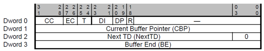
Figure 14-13 General Transfer Descriptor Format
Isochronous Transfer Descriptor
An Isochronous TD is used exclusively for isochronous endpoints. All TDs linked to an ED with F = 1 must use this format. This 32-byte structure must be aligned to a 32-byte boundary in system memory.
Figure 14-13 shows General Transfer Descriptor Format.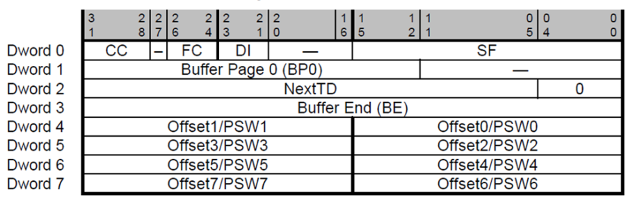
Figure 14-14 Isochronous Transfer Descriptor Format
14.5.2 EHCI Data Structure
The data structure definitions in this chapter support a 32-bit memory buffer address space. The interface consists of a Periodic Schedule, Periodic Frame List, Asynchronous Schedule, Isochronous Transaction Descriptors, Split-transaction Isochronous Transfer Descriptors, Queue Heads and Queue Element Transfer Descriptors.
Periodic Frame List
This schedule is for all periodic transfers (isochronous and interrupt). The periodic schedule is referenced from the operational registers space using the PeriodicListBase address register and the FRINDEX register. The periodic schedule is based on an array of pointers called the Periodic Frame List. The PeriodicListBase address register is combined with the FRINDEX register to produce a memory pointer into the frame list. The Periodic Frame List implements a sliding window of work over time.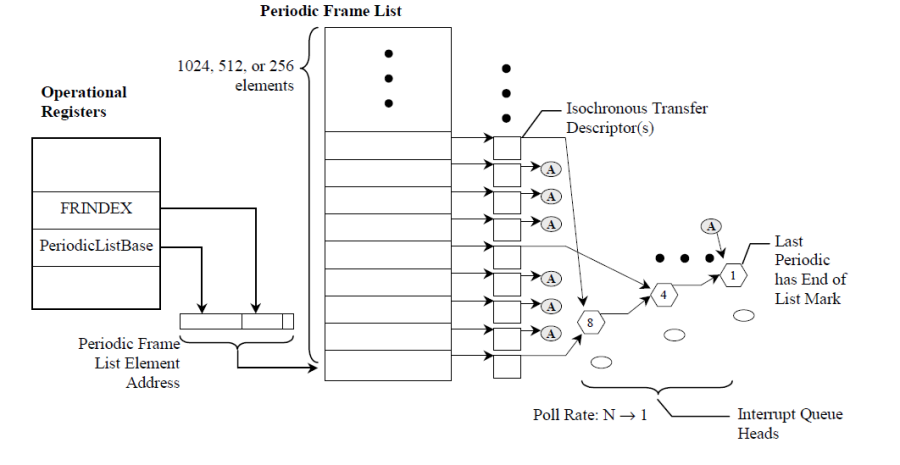
Figure 14-15 Periodic Frame List
Asynchronous List Queue Head Pointer
The Asynchronous Transfer List (based at the AsyncListAddr register), is where all the control and bulk transfers are managed. Host controllers use this list only when it reaches the end of the periodic list, the periodic list is disabled, or the periodic list is empty.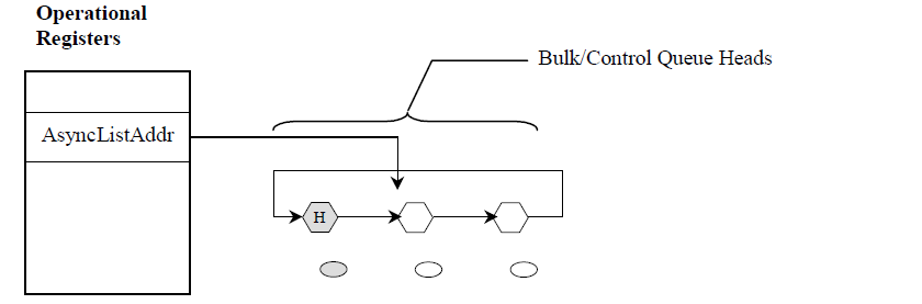
Figure 14-16 Asynchronous Transfer List
14.6 UTM Interface Timing Diagram
Figure 14-17 TX odd byte data
Figure 14-18 TX even byte data
Figure 14-19 RX odd byte data
Figure 14-20 RX even byte data
14.7 OHCI USB States
The Host Controller has four USB states visible to the Host Controller Driver via the Operational Registers: USBOPERATIONAL, USBRESET, USBSUSPEND, and USBRESUME. These states define the Host Controller responsibilities relating to USB signaling and bus states.
Figure 14-21 USB states
14.7.1 USBOPERATIONAL
When in the USBOPERATIONAL state, the Host Controller may process lists and will generate SOF Tokens. The USBOPERATIONAL state may be entered from the USBRESUME or USBRESET states. It may be exited to the USBRESET or USBSUSPEND states. When transitioning from USBRESET or USBRESUME to USBOPERATIONAL, the Host Controller is responsible for terminating the USB reset or resume signaling as defined in the USB Specification prior to sending a token.
14.7.2 USBRESET
When in the USBRESET state, the Host Controller forces reset signaling on the bus. The Host Controller's list processing and SOF Token generation are disabled while in USBRESET. The USBRESET state can be entered from any state at any time. The Host Controller defaults to the USBRESET state following a hardware reset. The Host Controller Driver is responsible for satisfying USB Reset signaling timing defined by the USB Specification.
14.7.3 USBSUSPEND
The USBSUSPEND state defines the USB Suspend state. The Host Controller's list processing and SOF Token generation are disabled. However, the Host Controller's remote wakeup logic must monitor USB wakeup activity. USBSUSPEND is entered following a software reset or from the USBOPERATIONAL state on command from the Host Controller Driver. While in USBSUSPEND, the Host Controller may force
a transition to the USBRESUME state due to a remote wakeup condition. This transition may conflict with the Host Controller Driver initiating a transition to the USBRESET state. If this situation occurs, the HCD-initiated transition to USBRESET has priority. The Host Controller Driver must wait 5 ms after transitioning to USBSUSPEND before transitioning to the USBRESUME state. Likewise, the Root Hub must wait 5 ms after the Host Controller enters USBSUSPEND before generating a local wakeup event and forcing a transition to USBRESUME. Following a software reset, the Host Controller Driver may cause a transition to USBOPERATIONAL if the transition occurs no more than 1 ms from the transition into USBSUSPEND. If the 1-ms period is violated, it is possible that devices on the bus will go into Suspend.
14.7.4 USBRESUME
When in the USBRESUME state, the Host Controller forces resume signaling on the bus. While in USBRESUME, the Root Hub is responsible for propagating the USB Resume signal to downstream ports as specified in the USB Specification. The Host Controller's list processing and SOF Token generation are disabled while in USBRESUME. USBRESUME is only entered from USBSUSPEND. The transition to USBRESUME can be initiated by the Host Controller Driver or by a USB remote wakeup signaled by the Root Hub. The Host
Controller is responsible for resolving state transition conflicts between the hardware wakeup and Host Controller Driver initiated state transitions. Legal state transitions from USBRESUME are to USBRESET and to USBOPERATIONAL. The Host Controller Driver is responsible for USB Resume signal timing as defined by the USB Specification.
14.8 USB OPERATION
14.8.1 OHCI Initialization
Initialize the open host controller, software should perform the following steps:
- Set software reset in Group1.1 UHO_HcControl register bit[7:6]=0.
- Configure OHCI command in Group1.1 UHO_HcControl register.
- Select routed all ports to OHCI by set 0 to bit0 of Group2.24 UHE_CONFIGFLAG register.
Note: Due to some devices on the USB that may take a long time to reset, it is desirable that the Host Controller Driver startup process not transition to the USBRESET state if possible.
14.8.2 EHCI Initialization
In order to initialize the enhanced host controller, software should perform the following steps:
- Set software reset in Group2.8 UHE_USBCMD register bit[1]=1.
- Program the Group2.12 UHE_CTRLDESSEGMENT register with 4-Gigabyte segment where all of the interface data structures are allocated.
- Write the appropriate value to the Group2.10 UHE_USBINTR register to enable the appropriate interrupts.
- Write the base address of the Periodic Frame List to the Group2.13 UHE_PERIODICLISTBASE register. Write the base address of the Asynchronous Frame List to the Group2.14 UHE_ASYNCLISTBASE register.
- Enable Periodic schedule in Gruop2.8 UHE_USBCMD register bit4, enable Asynchronous schedule in Gruop2.8 UHE_USBCMD register bit5.
- Write the Group2.8 UHE_USBCMD register to set the desired interrupt threshold, frame list size (if applicable).
- Write 1 to bit0 of Group2.24 UHE_CONFIGFLAG register to route all ports to the EHCI controller.
- Wait device connect by check Group2.25 UHE_PORTSC register bit0=1.
- Issue port reset by set Group2.25 UHE_PORTSC register bit8=1.
- Turn the host controller ON via setting the Run/Stop bit in Gruop2.8 UHE_USBCMD register bit0.
14.8.3 OTG Initialization
- Select work mode in Group8.0 MODE_SELECT register bit[1:0]. Default as 0 with OTG2.0.
- Confirm work role by read Group8.0 MODE_SELECT register bit[1:0] after "ID_CHANGE_IF" interrupt is assert. The ID_CHANGE_IF flag is in Group8.3 OTG_ST register bit1.
- Depend on work mode, set initial of OTG CTRL in Group8.1 OTG_DEVICE_CTRL register. Set SRP/ADP_SUPPORT in Group8.0 MODE_SELECT bit2 and bit3
- Set SRP/HNP/ADP related timers in Group8.4~8.29 registers.
14.9 Pattern of come to USB2.0
Define the line state J, K, SE0 of USB, that is, D+, D-, as shown in the following table.
J | K | SE0 | |
D+ | 1 | 0 | 0 |
D- | 0 | 1 | 0 |
USB 2.0 is made under the existing architecture that does not destroy USB1.1. Unless host and device are both 2.0, they are all transmitted with 1.1. The method of recognition is chirp, which is described as follows. The yellow line is D+ and the blue line is D-. The timing is as follows: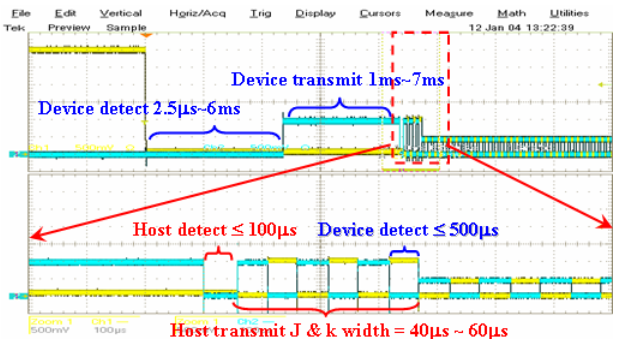
Figure 14-22 USB2.0 chirp pattern
- D+ pull up to 3.3V after device plug in
- Host drive bus reset (se0, both D+,D- = 0)
- Device chirp K 1ms-7ms. (D- = 800mV)
- Host chirp KJKJKJ sequence pattern
- Device recognizes 6 groups of kj and enters USB2.0 mode, turn on 45 Ohm pull down to GND at the same time, it make 800mV level become 400mV.
14.10 USB Interrupts
14.10.1 OHCI Interrupts
OHCI interrupt is from OHCI block with level signals. The detail interrupt information refer to the USBC0 Group1.3 bit[6:0] UHO_HcInterruptStatus Register. The enable register is USBC0 Group1.4 bit[6:0] UHO_HcInterruptEnable. Figure 14-23 shows the OHCI interrupt tree.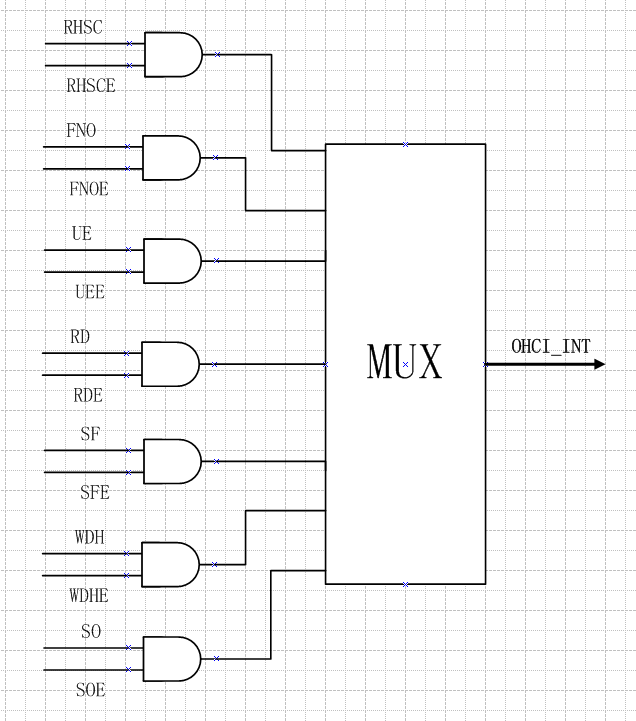
Figure 14-23 OHCI interrupt tree
- RHSC: Root Hub content change status bit
- FNO: Frame number overflow status bit
- UE: Un-recoverable error
- RD: Resume signaling detected status bit
- SF: Each start of a frame status bit
- WDH: HC has written HcDoneHead to HccaDoneHead status bit
- SO: USB schedule for the current Frame overruns status bit
14.10.2 EHCI Interrupts
EHCI interrupt is from EHCI block with level signals. The detail interrupt information refer to the USBC0 Group2.9 bit[5:0] UHE_USBSTS register. The enable register is USBC0 Group2.10 bit[5:0] UHE_USBINTR. Figure 14-24 shows the EHCI interrupt tree.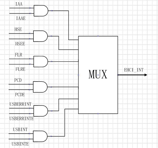
Figure 14-24 EHCI interrupt tree
- IAA: Indicates the assertion of Async Advance interrupt
- HSE: Host system error
- FLR: Indicate the Frame List Index rolls over from its maximum value to zero
- PCD: Indicate any port of the port owner bit is set to zero or from zero to a one
- USBERRINT: Indicate completion of a USB transaction results in an error condition
- USBINT: Indicate the completion of a USB transaction
14.10.3 OTG Interrupts
The detail OTG interrupt information refer to the USBC0 Group8.3 bit[9:0] OTG_ST register. The enable register is USBC0 Group8.2 bit[9:0] OTG_INT_EN. Figure 14-25 shows the OTG interrupt tree.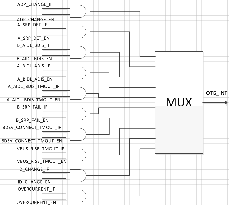
Figure 14-25 OTG interrupt tree
- ADP_CHANGE_IF: Indicate the ADP changed
- A_SRP_DET_IF: Indicate A-device(Host side) have detected SRP
- B_AIDL_BDIS_IF: Indicate B-device(Device side) disconnects to A-device(Host side) to start HNP
- A_BIDL_ADIS_IF: Indicate A-device(Host side) disconnects to B-device(Device side) to start HNP
- A_AIDL_BDIS_TMOUT_IF: Waiting for a disconnect timeout when HNP
- B_SRP_FAIL_IF: B-device SRP fail
- BDEV_CONNECT_TMOUT_IF: A-device waits B-device connect timeout
- VBUS_RISE_TMOUT_IF: A-device waits vbus valid timeout
- ID_CHANGE_IF: ID pin has changed
- OVERCURRENT_IF: An attached B-device draws more current
14.11 Registers Map
14.11.1 Registers Memory Map
Memory Map Start Address | Data Width | Group No. | Module |
|---|---|---|---|
0x9C004A80 | 32 | 149 | UPHY0 (USB PHY 0) |
0x9C004B00 | 32 | 150 | UPHY1 (USB PHY1) |
Table 14-1 USB PHY registers group list of RGST table
Both USB PHY registers have the same offset in corresponding register group. Only USB PHY0 (UPHY0) registers are described in following register description, for USB PHY1 please refer to UPHY0 description for more detail.
Memory Map Start Address | Data Width | Group No. | Module |
|---|---|---|---|
0x9C102000 | 32 | USBC0 Group 0 | USB0 HOST |
0x9C102080 | 32 | USBC0 Group 1 | USB0 OHCI |
0x9C102100 | 32 | USBC0 Group 2 | USB0 EHCI |
0x9C102400 | 32 | USBC0 Group 8 | USB0 OTG |
0x9C102800 | 32 | USBC0 Group 16 | USB0 DMA |
0x9C102880 | 32 | USBC0 Group 17 | USB0 INTERRUPT |
0x9C102900 | 32 | USBC0 Group 18 | USB0 EP0~4 |
0x9C102980 | 32 | USBC0 Group 19 | USB0 EP5/6/7 |
0x9C102A00 | 32 | USBC0 Group 20 | USB0 EP8/9/A/B |
0x9C102A80 | 32 | USBC0 Group 21 | USB0 EPC/D |
0x9C102B00 | 32 | USBC0 Group 22 | USB0 Phyclk Domain Interrupt |
0x9C102B80 | 32 | USBC0 Group 23 | USB0 Bulk Out FIFO |
0x9C103000 | 32 | USBC1 Group 0 | USB1 HOST |
0x9C103080 | 32 | USBC1 Group 1 | USB1 OHCI |
0x9C103100 | 32 | USBC1 Group 2 | USB1 EHCI |
0x9C103400 | 32 | USBC1 Group 8 | USB1 OTG |
0x9C103800 | 32 | USBC1 Group 16 | USB1 DMA |
0x9C103880 | 32 | USBC1 Group 17 | USB1 INTERRUPT |
0x9C103900 | 32 | USBC1 Group 18 | USB1 EP0~4 |
0x9C103980 | 32 | USBC1 Group 19 | USB1 EP5/6/7 |
0x9C103A00 | 32 | USBC1 Group 20 | USB1 EP8/9/A/B |
0x9C103A80 | 32 | USBC1 Group 21 | USB1 EPC/D |
0x9C103B00 | 32 | USBC1 Group 22 | USB1 Phyclk Domain Interrupt |
0x9C103B80 | 32 | USBC1 Group 23 | USB1 Bulk Out FIFO |
Table 14-2 USB control registers group list of AMBA table
Only USB0 relative register group will be described in register description, for USB1, please refer to USB0 corresponding group description for more detail
14.11.2 Registers Description
RGST Table Group 149 UPHY0
149.0 CONFIG0 (cfg0)
Address: 0x9C004A80
Reset: 0x0000 0080
| Field Name | Bit | Access | Description |
| Reserved | 31:8 | RO | RESERVED |
| J WAKE SEL | 7:5 | RW | J WAKE SEL controls wake up time. 0x0 : 0.54ms ˜ 1.09ms 0x1 : 1.09ms ˜ 1.68ms 0x2 : 1.68ms ˜ 2.18ms 0x3 : 2.18ms ˜ 2.73ms 0x4 : 2.73ms ˜ 3.27ms(default) 0x5 : 3.27ms ˜ 3.82ms 0x6 : 4.36ms ˜ 4.91ms 0x7 : 4.91ms ˜ 5.46ms |
| J ANG LB | 4 | RW | Analog Loopback mode. 0x0 : turn off analog loopback(default). 0x1 : turn on analog loopback. |
| J DIG LB | 3 | RW | Digital Loopback mode. 0x0 : turn off digital loopback(default). 0x1 : turn on digital loopback. |
J IPX2 | 2 | RW | Charge Pump Current Option. |
J ENABLE CNTR | 1 | RW | Bist mode counter enable of succcess and fail. |
J CLEAR CNTR | 0 | RW | Bist mode counter clear of succcess and fail. |
149.1 CONFIG1 (cfg1)
Address: 0x9C004A84
Reset: 0x0000 0021
| Field Name | Bit | Access | Description |
| Reserved | 31:8 | RO | RESERVED |
| J HS TX DELAY | 7:6 | RW | Fine tune TX Delay 0x0 : No delay(default). 0x1 : Delay 1 clock. 0x2 : Delay 2 clock. 0x3 : No delay. |
| J HS TX PWRSAV | 5 | RW | High Speed TX power saving. When this item actives, it means TX driver will turn on with TXValid. When this item is low, it means TX driver will always turn on. |
| J HS RX DROP2 | 4 | RW | Set the EOP receive condition sensitive If DEV_DET fall very quickly, this may cause some valid EOP bit lose and cause correct packet become RXERROR, so this register set medium EOP detection. 0x0: do nothing(default) |
| J HS RX DROP4 | 3 | RW | Set the EOP receive condition very sensitive If DEV_DET fall very quickly, this may cause some valid EOP bit lose and cause correct packet become RXERROR, so this register set very sensitive EOP detection. 0: do nothing(default) |
| J HS RX LPFIL | 2:1 | RW | CDR data channel phase shift precision 0x0: shift precision is very high 0x1: shift precision is high 0x2: shift precision is medium 0x3: shift precision is slow |
| J FS TX PREDR IDLE | 0 | RW | For 1st cross over point perfection 0: Disable(default) 1 : Enable |
149.2 CONFIG2 (cfg2)
Address: 0x9C004A88
Reset: 0x0000 0000
| Field Name | Bit | Access | Description |
| Reserved | 31:8 | RO | RESERVED |
| J DPN | 7:4 | RW | DP Full speed falling time select. The larger the value, the shorter the DP falling transition time. Default: 4'b0000 |
| J DPP | 3:0 | RW | DP Full speed rising time select. The larger the value, the shorter the DP rising transition time. Default: 4'b0000 |
149.3 CONFIG3 (cfg3)
Address: 0x9C004A8C
Reset: 0x0000 0021
Field Name | Bit | Access | Description |
Reserved | 31:8 | RO | RESERVED |
J FORCE PU2 HI | 7 | RW | J FORCE PU2 HI |
J FORCE PU2 LO | 6 | RW | J FORCE PU2 LO |
J FORCE DISC ON | 5 | RW | Whenever DPDM PULLDOWN, the system force into chirp mode |
| DEBUG_INT | 4:0 | RW | Reserved for internal debug purpose. Access to this register may cause unexpected malfunction |
149.4 CONFIG4 (cfg4)
Address: 0x9C004A90
Reset: 0x0000 0020
| Field Name | Bit | Access | Description |
| Reserved | 31:8 | RO | RESERVED |
| J IPX3 | 7 | RW | Charge Pump Current Option. macro spec. |
| J IPX1 | 6 | RW | Charge Pump Current Option. macro spec. |
J SKIP NOXTION | 5 | RW | J SKIP NOXTION |
J PGMODE | 4:0 | RW | Pattern Selection of bist test |
149.5 CONFIG5 (cfg5)
Address: 0x9C004A94
Reset: 0x0000 0000
Field Name | Bit | Access | Description |
Reserved | 31:8 | RO | RESERVED |
SUCC CNTR | 7:4 | RU | Bit mode success counter When successive 15 packages success, BIST test success and done. |
FAIL CNTR | 3:0 | RU | Bit mode fail counter When successive 15 packages fail, BIST test fail and done. |
149.6 CONFIG6 (cfg6)
Address: 0x9C004A98
Reset: 0x0000 0000
| Field Name | Bit | Access | Description |
| Reserved | 31:8 | RO | RESERVED |
| J DMN | 7:4 | RW | DM Full speed falling time select. The larger the value, the shorter the DP falling transition time. Default: 4'b0000 |
| J DMP | 3:0 | RW | DM Full speed rising time select. The larger the value, the shorter the DP rising transition time. Default: 4'b0000 |
149.7 CONFIG7 (cfg7)
Address: 0x9C004A9C
Reset: 0x0000 008A
| Field Name | Bit | Access | Description |
| Reserved | 31:8 | RO | RESERVED |
| J EN INR | 7 | RW | Internal Rext function enable 0x0 : disable 0x1 : enable(default) |
| J R TRIM | 6:5 | RW | Loop filter R trim table {R TRIM1,R TRIM0} 0x0 : 80K 0x1 : 18K 0x2 : 16K 0x3 : 14K |
| J DISC | 4:0 | RW | control disconnect voltage(16.5mV/step) 0x00 : value 405mv. 0x0a : value 570mv(default). 0x1e : 900mv. 0x1f : Disable Disconnection |
149.8 CONFIG8 (cfg8)
Address: 0x9C004AA0
Reset: 0x0000 0000
Field Name | Bit | Access | Description |
Reserved | 31:8 | RO | RESERVED |
J FS TX J DELAY | 7:6 | RW | Full speed DP delay cycle |
J FS TX K DELAY | 5:4 | RW | Full speed DM delay cycle |
J LS TX J DELAY | 3:2 | RW | Low speed DP delay cycle |
J LS TX K DELAY | 1:0 | RW | Low speed DM delay cycle |
149.9 CONFIG9 (cfg9)
Address: 0x9C004AA4
Reset: 0x0000 0006
| Field Name | Bit | Access | Description |
| Reserved | 31:5 | RO | RESERVED |
| J FL FORCE FS | 4 | RW | Enable Config device error state 0 : enable error state(default) |
| J FL DP PILLUP | 3 | RW | Config device DP or MP resister pullup 0 : Full-low speed DP pull up(default) |
| J FL SAMPLE SEL | 2 | RW | Enable Full-low speed rx linestat sample circuit 0 : disable Full-low speed rx linestat sample circuit |
| J DIS FSM WAIT4MS EN | 1 | RW | Disable HOSTDISC error state 0 : enable error state 1 : disable error state(default) |
| J FS ONLY | 0 | RW | Disable UPHY AFE Low speed circuit at Low speed 0 : Low speed circuit use in Low speed(default) 1 : Full speed circuit usb in Low speed |
149.10 CONFIG10 (cfg10)
Address: 0x9C004AA8
Reset: 0x0000 0000
| Field Name | Bit | Access | Description |
| Reserved | 31:8 | RO | RESERVED |
| NA | 7 | RO | High speed disconnect signal with filter. 0 : disconnect is not happened(default) 1 : disconnect is happened |
J HSDISC LPFILTER | 6:4 | RW | High speed disconnect filter number |
J ALDISC OFF | 3 | RW | Host disconnect force 0 |
J ALDISC ON | 2 | RW | Host disconnect force 1 |
J HSDISC OFF | 1 | RW | High speed disconnect force 0 |
J HSDISC ON | 0 | RW | High speed disconnect force 1 |
149.11 CONFIG11 (cfg11)
Address: 0x9C004AAC
Reset: 0x0000 0000
| Field Name | Bit | Access | Description |
| Reserved | 31:8 | RO | RESERVED |
| LINESTATE | 7:6 | RO | Linestate signal without control 0x0 : SE0 state(default). 0x1 : J state. 0x2 : K state. 0x3 : SE1 state. |
| Reserved | 5:3 | RO | RESERVED |
| J LINE EN | 2 | RW | Force Linestate signal 0 : disable force linestate(default). 1 : force linestate. |
| J LINE DATA | 1:0 | RW | Force Linestate signal value 0x0 : SE0 state(default). 0x1 : J state. 0x2 : K state. 0x3 : SE1 state. |
149.12 CONFIG12 (cfg12)
Address: 0x9C004AB0
Reset: 0x0000 0007
| Field Name | Bit | Access | Description |
| Reserved | 31:0 | RO | Reserved for Industrial Debug Purpose |
149.13 CONFIG13 (cfg13)
Address: 0x9C004AB4
Reset: 0x0000 0000
Field Name | Bit | Access | Description |
DEBUG_INT | 31:0 | RU | Reserved for Industrial Debug Purpose |
149.14 CONFIG14 (cfg14)
Address: 0x9C004AB8
Reset: 0x0000 0011
| Field Name | Bit | Access | Description |
| Reserved | 31:5 | RO | RESERVED |
PHY R CONFIG | 4 | RW | UPHY resume config mode |
FS/LS RX DCP | 3:2 | RW | FS/LS RX data capture point |
FS/LS RX SCP | 1:0 | RW | FS/LS RX SYNC capture point |
149.15 CONFIG15 (cfg15)
Address: 0x9C004ABC
Reset: 0x0000 0000
| Field Name | Bit | Access | Description |
| Reserved | 31:2 | RO | RESERVED |
| HS DIS DG FLT | 1:0 | RW | High speed disconnect de-glitch filter 0x0 : no de-glitch(default). 0x1 : 1 time de-glitch. 0x2 : 2 time de-glitch. 0x3 : NA |
149.16 CONFIG16 (cfg16)
Address: 0x9C004AC0
Reset: 0x0000 0000
| Field Name | Bit | Access | Description |
| Reserved | 31:8 | RO | RESERVED |
J FORCE VDM SRC | 7 | RW | FORCE DM voltage. |
J TBCWAIT[1:0] | 6:5 | RW | Battery charger disconnect to rework time. |
J TVDM SRC DIS[1:0] | 4:3 | RW | J Battery charger polling DP high to send dm voltage time. |
J TVDM SRC EN[1:0] | 2:1 | RW | Battery charger polling DP low to disable dm voltage time. |
J BC ENABLE | 0 | RW | Battery Charger CDP Function Enable. |
149.17 CONFIG17 (cfg17)
Address: 0x9C004AC4
Reset: 0x0000 0092
| Field Name | Bit | Access | Description |
| Reserved | 31:8 | RO | RESERVED |
IBG TRIM0[2:0] | 7:5 | RW | Current of current source in CDP mode. 0x0f : TTNVNT (default) I=100uA 0x12 : FFHVLT 0x0a : FFHVHT 0x17 : SSHVLT 0x0c : SSLVHT 0x17 : SSLVLT |
J VDATREF TRIM[3:0] | 4:1 | RW | Reference voltage of comparator in CDP mode. VDATREF TRIM[3:0] 0x1 : 250mv 0x2 : 300mv 0x4 : 350mv 0x8 : 400mv 0x9 : default |
J EN DCP | 0 | RW | Battery Charger DCP Function Enable. 0 : disable DCP(default) 1 : enable DCP |
149.18 CONFIG18 (cfg18)
Address: 0x9C004AC8
Reset: 0x0000 0010
| Field Name | Bit | Access | Description |
| Reserved | 31:8 | RO | RESERVED |
| BC DETECT STATUS | 7 | RW | Indicate Battery Charge handshake status 0:BC handshake done(default), 1:BC handshake is in progress. |
| VDMSRC TRIM[4:0] | 6:2 | RW | Dm source voltage. 0x01 : 500mv 0x02 : 550mv 0x04 : 600mv(default) 0x08 : 650mv 0x10 : 700mv |
| IBG TRIM1[1:0] | 1:0 | RW | Current of current source in CDP mode. 0x0f : TTNVNT (default) I=100uA 0x12 : FFHVLT 0x0a : FFHVHT 0x17 : SSHVLT 0x0c : SSLVHT 0x17 : SSLVLT |
149.19 CONFIG19 (cfg19)
Address: 0x9C004ACC
Reset: 0x0000 0000
Field Name | Bit | Access | Description |
Reserved | 31:1 | RO | RESERVED |
EN HSRXACTIVE INT | 0 | RW | Enable UPHY Interrupt. |
149.20 CONFIG20 (cfg20)
Address: 0x9C004AD0
Reset: 0x0000 0009
| Field Name | Bit | Access | Description |
| Reserved | 31:8 | RO | RESERVED |
Reserved | 7 | RW | RESERVED |
Reserved | 6 | RW | RESERVED |
NA | 5:0 | RW | NA |
J AC2 0 B | 5:3 | RW | OTG Discharge Current Option. 0x0: 5uA 0x1: 10uA 0x2: 15uA 0x3: 20uA 0x4: 30uA (default) 0x5: 40uA 0x6: 50uA 0x7: 60uA |
J AC2 0 | 2:0 | RW | OTG Charge Current Option. 0x0: 5uA 0x1: 10uA 0x2: 15uA 0x3: 20uA 0x4: 30uA (default) 0x5: 40uA 0x6: 50uA 0x7: 60uA |
149.21 CONFIG21 (cfg21)
Address: 0x9C004AD4
Reset: 0x0000 0001
Field Name | Bit | Access | Description |
Reserved | 31:8 | RO | RESERVED |
BC DETECT STS | 7 | RO | Battery Charge is in detect progress. |
BC PRTBL STS | 6 | RO | Battery Charge successful detect PRTBL STS. |
BC VDMSRC STS | 5 | RO | Battery Charge successful send VDM SRC. |
BC DISC CNT | 4:3 | RO | Battery Charge detect disconnect counter. |
BC SUCC CNT | 2:1 | RO | Battery Charge handshake successful counter. |
J BC SUSPEND EN | 0 | RW | Enable Battery Charge handshake while PHY in SUSPEND MODE. |
149.22 CONFIG22 (cfg22)
Address: 0x9C004AD8
Reset: 0x0000 0077
Field Name | Bit | Access | Description |
Reserved | 31:8 | RO | RESERVED |
DCP2P7V | 7:4 | RW | Battery Charge DCP 2.7V control to APHY DCP 1.2V mode dm source voltage trimming: triming step=25mV 0x0: 1.025V 0x3: 1.1V 0x7: 1.2V 0xb: 1.3V 0xe: 1.4V |
DCP1P2V | 3:0 | RW | Battery Charge DCP 1.2V control to APHY DCP 2.7V mode dm source voltage trimming: triming step=25mV 0x0: 2.525V 0x3: 2.6V 0x7: 2.7V 0xb: 2.8V 0xe: 2.9V |
149.23 CONFIG23 (cfg23)
Address: 0x9C004ADC
Reset: 0x0000 0018
| Field Name | Bit | Access | Description |
Reserved | 31:8 | RO | RESERVED |
RFU | 7:6 | RW | Reserved for future use |
PROB | 5:3 | RW | APHY Probe control 0x0: 597.5mV 0x1: 617.5mV 0x2: 636.5mV 0x3: 656.5mV (default) 0x4: 675.5mV 0x5: 695.5mV 0x6: 714.5mV 0x7: 734.5mV |
R TEST TIEH | 2 | RW | R TEST Tie High control to APHY 0: disable (default) 1: USB_R_TEST=AVDDC33 |
EN DCP2P7V | 1 | RW | Enable 2.7V DCP mode 0: disable 2.7V DCP mode (default) 1: enable 2.7V DCP mode |
EN DCP1P2V | 0 | RW | Enable 1.2V DCP mode 0: disable 1.2V DCP mode (default) 1: enable 1.2V DCP mode |
149.24 CONFIG24 (cfg24)
Address: 0x9C004AE0
Reset: 0x0000 0001
| Field Name | Bit | Access | Description |
| Reserved | 31:8 | RO | RESERVED |
| BC AUTO RST | 7 | RW | Battery Charge auto re-start enable 1'b0: Disable auto re-start. 1'b1: Enable auto re-start(Default) |
| TBC AUTO RST | 6:0 | RW | Battery Charge auto re-start timer When counter equal to J_TBC_AUTO_RST, internal FSM timeout. Real time is 606ms*J_TBC_AUTO_RST |
149.25 CONFIG25 (cfg25)
Address: 0x9C004AE4
Reset: 0x0000 0004
| Field Name | Bit | Access | Description |
| Reserved | 31:8 | RO | RESERVED |
| RFU | 7:3 | RW | Reserved for future use |
| SQ CT | 2:0 | RW | RX Squelch level control to APHY 0x0: 67.8mV 0x1: 84.5mV 0x2: 101.2mV 0x3: 118.1mV 0x4: 135.0mV (default) 0x5: 152.1mV 0x6: 169.2mV 0x7: 186.6mV |
USB Controller System 0 (USBC0)
Group 0 USB Host Control (UHC)
0.0 USB Host Version (UHVERSION)
Address: 0x9C102000
Reset: 0xC2120101
| Field Name | Bit | Access | Description |
| UHVERSION | 31:0 | RO | USB Host Hardware Version Read as '0xC2120101' |
0.4 USB Power Control and Status (UHPOWERCS PORT)
Address: 0x9C102010
Reset: 0x00070000
| Field Name | Bit | Access | Description |
reserved | 31:19 | RO | RESERVED |
UPHY SUSPENDM | 18 | RO | UPHY Suspend Signal |
UPHY PARTIALM | 17 | RO | UPHY Partial Signal |
USB CLK EN | 16 | RO | USB Clock Enable |
reserved | 15:12 | RO | RESERVED |
UPHY PAR EN | 11 | RW | UPHY Partial Enable |
UPHY SUSP EN | 10 | RW | UPHY Suspend Enable |
UPHY PAR CTRL | 9 | RW | UPHY Partial Control |
UPHY SUSP CTRL | 8 | RW | UPHY Suspend Control |
reserved | 7:2 | RO | RESERVED |
USBCLK SEL | 1 | RW | USB Clock Domain Clock Select |
reserved | 0 | RO | RESERVED |
Group 1 USB Host OHCI Controller
1.0 OHCI HcRevision Register (UHO HcRevision)
Address: 0x9C102080
Reset: 0x00000010
Field Name | Bit | Access | Description |
Reserved | 31:8 | RO | Reserved |
REV | 7:0 | RO | OHCI Revision |
1.1 OHCI HcControl Register (UHO HcControl)
Address: 0x9C102084
Reset: 0x00000000
| Field Name | Bit | Access | Description |
| Reserved | 31:11 | RO | Reserved |
| RWE | 10 | RO | RemoteWakeupEnable This bit is used by HCD to enable or disable the remote wakeup signaling upon the detection of upstream resume. read as '0' |
| RWC | 9 | RO | RemoteWakeupConnected This bit indicates whether HC supports remote wakeup signaling, read as '0' |
| IR | 8 | RW | InterruptRouting Not support. |
| HCFS | 7:6 | RW | HostControllerFunctionalState for USB 0x0 : USBRESET (default) 0x1 : USBRESUME 0x2 : USBOPERATIONAL 0x3 : USBSUSPEND |
| BLE | 5 | RW | BulkListEnable Enable or disable the processing of the Bulk list in the next frame. Default disabled |
CLE | 4 | RW | ControlListEnable |
IE | 3 | RW | IsochronousEnable |
PLE | 2 | RW | PeriodicListEnable |
CBSR | 1:0 | RW | ControlBulkServiceRatio |
1.2 OHCI HcCommandStatus Register (UHO HcCommandStatus)
Address: 0x9C102088
Reset: 0x00000000
| Field Name | Bit | Access | Description |
| Reserved | 31:18 | RO | Reserved |
| SOC | 17:16 | RO | SchedulingOverrunCount Used by HCD to monitor any persistent scheduling problems. |
| Reserved | 15:4 | RO | Reserved |
| OCR | 3 | RO | OwnershipChangeRequest Not support |
| BLF | 2 | RW | BulkListFilled Indicate whether there are any TDs on the Bulk list. 1: There is TDs on the Bulk list. 0: There is no TDs on the Bulk list (default) |
| CLF | 1 | RW | ControlListFilled Indicate whether there are any TDs on the Control list. 1: There is TDs on the Control list. 0: There is no TDs on the Control list (default |
| HCR | 0 | other | HostControllerReset Write 1, host Controller software reset, then clear this field by itself. |
1.3 OHCI HcInterruptStatus Register (UHO HcInterruptStatus)
Address: 0x9C10208C
Reset: 0x00000000
Field Name | Bit | Access | Description |
Reserved | 31 | RO | Reserved |
OC | 30 | RO | OwnershipChange |
Reserved | 29:7 | RO | Reserved |
RHSC | 6 | RWC | RootHubStatusChange |
FNO | 5 | RWC | FrameNumberOverflow |
UE | 4 | RWC | UnrecoverableError |
RD | 3 | RWC | ResumeDetected |
SF | 2 | RWC | StartofFrame |
WDH | 1 | RWC | WritebackDoneHead |
SO | 0 | RWC | SchedulingOverrun |
1.4 OHCI HcInterruptEnable Register (UHO HcInterruptEnable)
Address: 0x9C102090
Reset: 0x00000000
Field Name | Bit | Access | Description |
MIE | 31 | Other | MasterInterruptEnable |
OC | 30 | RO | OwnershipChange |
Reserved | 29:7 | RO | Reserved |
RHSC | 6 | Other | RootHubStatusChange |
FNO | 5 | Other | FrameNumberOverflow |
UE | 4 | Other | UnrecoverableError |
RD | 3 | Other | ResumeDetected |
SF | 2 | Other | StartofFrame |
WDH | 1 | Other | WritebackDoneHead |
SO | 0 | Other | SchedulingOverrun |
1.5 OHCI HcInterruptDisable Register (UHO HcInterruptDisable)
Address: 0x9C102094
Reset: 0x00000000
Field Name | Bit | Access | Description |
MIE | 31 | Other | MasterInterruptEnable |
OC | 30 | RO | OwnershipChange |
Reserved | 29:7 | RO | Reserved |
RHSC | 6 | Other | RootHubStatusChange |
FNO | 5 | Other | FrameNumberOverflow |
UE | 4 | Other | UnrecoverableError |
RD | 3 | Other | ResumeDetected |
SF | 2 | Other | StartofFrame |
WDH | 1 | Other | WritebackDoneHead |
SO | 0 | Other | SchedulingOverrun |
1.6 OHCI HcHCCA Register (UHO HcHCCA)
Address: 0x9C102098
Reset: 0x00000000
Field Name | Bit | Access | Description |
HCCA | 31:8 | RW | Host Controller Communication Area |
Reserved | 7:0 | RO | Reserved |
1.7 OHCI HcPeriodCurrentED Register (UHO HcPeriodCurrentED)
Address: 0x9C10209C
Reset: 0x00000000
Field Name | Bit | Access | Description |
PCED | 31:4 | RO | PeriodCurrentED |
Reserved | 3:0 | RO | Reserved |
1.8 OHCI HcControlHeadED Register (UHO HcControlHeadED)
Address: 0x9C1020A0
Reset: 0x00000000
Field Name | Bit | Access | Description |
CHED | 31:4 | RW | ControlHeadED |
Reserved | 3:0 | RO | Reserved |
1.9 OHCI HcControlCurrentED Register (UHO HcControlCurrentED)
Address: 0x9C1020A4
Reset: 0x00000000
Field Name | Bit | Access | Description |
CCED | 31:4 | RW | ControlCurrentED |
Reserved | 3:0 | RO | Reserved |
1.10 OHCI HcBulkHeadED Register (UHO HcBulkHeadED)
Address: 0x9C1020A8
Reset: 0x00000000
Field Name | Bit | Access | Description |
BHED | 31:4 | RW | BulkHeadED |
Reserved | 3:0 | RO | Reserved |
1.11 OHCI HcBulkCurrentED Register (UHO HcBulkCurrentED)
Address: 0x9C1020AC
Reset: 0x00000000
Field Name | Bit | Access | Description |
BCED | 31:4 | RW | BulkCurrentED |
Reserved | 3:0 | RO | Reserved |
1.12 OHCI HcDoneHead Register (UHO HcDoneHead)
Address: 0x9C1020B0
Reset: 0x00000000
Field Name | Bit | Access | Description |
DH | 31:4 | RO | DoneHead |
Reserved | 3:0 | RO | Reserved |
1.13 OHCI HcFmInterval Register (UHO HcFmInterval)
Address: 0x9C1020B4
Reset: 0x27782EDF
| Field Name | Bit | Access | Description |
| FIT | 31 | RW | FrameIntervalToggle HCD toggles this bit whenever it loads a new value to FrameInterval. |
| FSMPS | 30:16 | RW | FSLargestDataPacket Default value is (FI-210)*6/7 |
| Reserved | 15:14 | RO | Reserved |
| FI | 13:0 | RW | Frame Interval Specify the interval between two consecutive SOFs in 12MHz. The nominal value is set to be 11,999. |
1.14 OHCI HcFmRemaining Register (UHO HcFmRemaining)
Address: 0x9C1020B8
Reset: 0x00000000
| Field Name | Bit | Access | Description |
| FRT | 31 | RO | Frame Remaining Toggle This bit is loaded from the FrameIntervalToggle field of HcFmInterval whenever FrameRemaining reaches 0. |
| Reserved | 30:15 | RO | Reserved |
| FR | 14:0 | RO | Frame Remaining When it reaches zero, it is reset by loading the FrameInterval value specified in HcFmInterval at the next bit time boundary. |
1.15 OHCI HcFmNumber Register (UHO HcFmNumber)
Address: 0x9C1020BC
Reset: 0x00000000
| Field Name | Bit | Access | Description |
| Reserved | 31:16 | RO | Reserved |
| FN | 15:0 | RO | FrameNumber |
1.16 OHCI HcPeriodicStart Register (UHO HcPeriodicStart)
Address: 0x9C1020C0
Reset: 0x00000000
| Field Name | Bit | Access | Description |
| Reserved | 31:15 | RO | Reserved |
| PS | 14:0 | RW | PeriodicStart When HcFmRemaining reaches the value specified,processing of the periodic lists will have priority over Control/Bulk pro- cessing. |
1.17 OHCI HcLSThreshold Register (UHO HcLSThreshold)
Address: 0x9C1020C4
Reset: 0x00000628
Field Name | Bit | Access | Description |
Reserved | 31:8 | RO | Reserved |
LST | 7:0 | RW | LSThreshold |
1.18 OHCI HcRhDescriptorA Register (UHO HcRhDescriptorA)
Address: 0x9C1020C8
Reset: 0x01000101
| Field Name | Bit | Access | Description |
| POTPGT | 31:24 | RO | PowerOnToPowerGoodTime Not support |
| Reserved | 23:13 | RO | Reserved |
| NOCP | 12 | RO | NoOverCurrentProtection Read as '1', Not overcurrent protection support |
| OCPM | 11 | RO | OverCurrentProtectionMode Read as '0', Not support |
| DT | 10 | RO | DeviceType Read as '0', specified that the Root Hub is not a compound device. |
| NPS | 9 | RO | NoPowerSwitching Read as '1', ports are always powered on |
| PSM | 8 | RO | PowerSwitchingMode Read as '0', all ports are powered at the same time |
| NDP | 7:0 | RO | NumberDownstreamPorts The number of downstream ports supported by the Root Hub is 8'b1 |
1.19 OHCI HcRhDescriptorB Register (UHO HcRhDescriptorB)
Address: 0x9C1020CC
Reset: 0x00000000
| Field Name | Bit | Access | Description |
| PPCM | 31:16 | RO | PortPowerControlMask Not support, read as 0x00 |
| DR | 15:0 | RW | DeviceRemovable Not support, read as 0x00 |
1.20 OHCI HcRhStatus Register (UHO HcRhStatus)
Address: 0x9C1020D0
Reset: 0x00000000
| Field Name | Bit | Access | Description |
| CRWE | 31 | Other | (write) ClearRemoteWakeupEnable Writing a '1' clears DeviceRemoveWakeupEnable. Writing a '0' has no effect. |
| Reserved | 30:18 | RO | Reserved |
| CCIC | 17 | RO | OverCurrentIndicatorChange Not support |
| LPSC | 16 | RO | (read) LocalPowerStatusChange Read as '0', the Root Hub does not support the local power status feature (write) SetGlobalPower Not support. |
| DRWE | 15 | RW | (read) DeviceRemoteWakeupEnable This bit enables a ConnectStatusChange bit as a resume event, causing a USBSUSPEND to USBRESUME state tran- sition and setting the ResumeDetected interrupt. 0 = ConnectStatusChange is not a remote wakeup event. (default) 1 = ConnectStatusChange is a remote wakeup event. (write) SetRemoteWakeupEnable Writing a '1' sets De- viceRemoveWakeupEnable. Writing a '0' has no effect. |
| Reserved | 14:2 | RO | Reserved |
| OCI | 1 | RO | OverCurrentIndicator Read as '0', Not support |
| LPS | 0 | RO | (read) LocalPowerStatus Read as '0', the Root Hub does not support the local power status feature (write) ClearGlobalPower Not support |
1.21 OHCI HcRhPortStatus Register (UHO HcRhPortStatus)
Address: 0x9C1020D4
Reset: 0x00000100
| Field Name | Bit | Access | Description |
| Reserved | 31:21 | RO | Reserved |
| PRSC | 20 | W1C | PortResetStatusChange 0 = port reset is not complete 1 = port reset is complete |
| OCIC | 19 | RO | PortOverCurrentIndicatorChange Read as '0', no change in PortOverCurrentIndicator |
| PSSC | 18 | W1C | PortSuspendStatusChange 0 = resume is not completed 1 = resume completed |
| PESC | 17 | W1C | PortEnableStatusChange 0 = no change in PortEnableStatus 1 = change in PortEnableStatus |
| CSC | 16 | W1C | ConnectStatusChange 0 = no change in CurrentConnectStatus 1 = change in CurrentConnectStatus |
| Reserved | 15:10 | RO | Reserved |
| LSDA | 9 | Other | (read) LowSpeedDeviceAttached Indicates the speed of the device attached to this port. This field is valid only when the CurrentConnectStatus is set. 0 = full speed device attached 1 = low speed device attached (write) ClearPortPower HCD clears the PortPowerStatus bit by writing a '1' to this bit.Writing a '0' has no effect. |
| PPS | 8 | RO | (read) PortPowerStatus Read as '1', port power is on. (write) SetPortPower HCD writes a '1' to set the PortPowerStatus bit. Writing a '0' has no effect. |
| Reserved | 7:5 | RO | Reserved |
| PRS | 4 | Other | (read) PortResetStatus 0 = port reset signal is not active 1 = port reset signal is active (write) SetPortReset HCD sets the port reset signaling by writing a '1' to this bit.Writing a '0' has no effect. |
| POCI | 3 | Other | (read) PortOverCurrentIndicator Read as '0', no overcurrent condition (write) ClearSuspendStatus HCD writes a '1' to initiate a resume. Writing a '0' has no effect. A resume is initiated only if PortSuspendStatus is set. |
| PSS | 2 | Other | (read) PortSuspendStatus Indicate the port is suspended or in the resume sequence. 0 = port is not suspended 1 = port is suspended (write) SetPortSuspend The HCD sets the PortSuspendSta- tus bit by writing a '1' to this bit. Writing a '0' has no effect. |
| PES | 1 | Other | (read) PortEnableStatus Indicate whether the port is enabled or disabled. HCD sets this bit by writing SetPortEnable and clears it by writing ClearPortEnable. 0 = port is disabled 1 = port is enabled (write) SetPortEnable The HCD sets PortEnableStatus by writing a '1'.Writing a '0' has no effect. |
| CCS | 0 | Other | (read) CurrentConnectStatus 0 = no device connected 1 = device connected (write) ClearPortEnable 0 = Ignore 1 = clear the PortEnableStatus bit Note: This bit is always read '1b' when the attached device is nonremovable (DeviceRemoveable[NDP]). |
1.25 HcRhPortStatus Additional Register (UH PortStatusA)
Address: 0x9C1020E4
Reset: 0x00180B40
| Field Name | Bit | Access | Description |
| reserved | 31:23 | RO | RESERVED |
| CLK DIV2 5 | 22:16 | RW | Clock Divider for 2.5us from Slow Clock These bits are used to divide the slow clock to 2.5us pulse for remote wakeup use. default '24' for 10MHz clock |
| reserved | 15:12 | RO | RESERVED |
SAMPLE EN | 11 | RW | UTMI RX Negedge Sample Enable |
RXERR BLOCK EN | 10 | RW | PHY RXERR Signal Block Enable |
OUT TRIG | 9:8 | RW | OUT Transfer Trigger Level |
PHY SIM MODE | 7 | RW | PHY Simulation Mode |
LS TO CTRL | 6:4 | RW | Low Speed Timeout Control |
PORT PAR EN | 3 | RW | PHYCLK is able to stop in SUSPEND State |
reserved | 2:1 | RO | Reserved |
SUSPEND HCFS | 0 | RW | Suspend when HC in suspend state |
Group 2 USB Host EHCI Controller
2.0 EHCI Interface Version Number (UHE HCIVERSION)
Address: 0x9C102100
Reset: 0x01100020
| Field Name | Bit | Access | Description |
| HCIVERSION | 31:16 | RO | Interface Version Number The most significant byte of this register represents a major revision and the least significant byte is the minor revision. Read as '0110' |
| Reserved | 15:8 | RO | Reserved |
| CAPLENGTH | 7:0 | RO | Capability Register Length offset to add to register base to find the beginning of the Operational Register Space. Read as '20' |
2.1 EHCI Structural Parameters (UHE HCSPARAMS)
Address: 0x9C102104
Reset: 0x00001101
| Field Name | Bit | Access | Description |
| Reserved | 31:24 | RO | Reserved |
| DPN | 23:20 | RO | Debug Port Number |
| Reserved | 19:17 | RO | Reserved |
| P INDICATOR | 16 | RO | Port Indicators Not support, read as '0' |
| N CC | 15:12 | RO | Number of Companion Controller Read as '1', indicates the number of companion controllers associated with this USB 2.0 host controller. |
| N PCC | 11:8 | RO | Number of Ports per Companion Controller Read as '1', indicates the number of ports supported per companion host controller. |
PRR | 7 | RO | Port Routing Rules the next N PCC port are routed to the next lowest function com- panion controller, and so on. |
Reserved | 6:5 | RO | Reserved |
PPC | 4 | RO | Port Power Control |
N PORTS | 3:0 | RO | Number of PORTS |
2.2 EHCI Capability Parameters (UHE HCCPARAMS)
Address: 0x9C102108
Reset: 0x000A0006
| Field Name | Bit | Access | Description |
| Reserved | 31:20 | RO | Reserved |
| 32FPLC | 19 | RO | 32-Frame Periodic List Capability Read as '1', indicates 32-Frame Periodic List Capability is supported |
| PPCEC | 18 | RO | Per-Port Change Event Capability Read as '0', indicates per-port change event is not sup- ported |
| LPMC | 17 | RO | Link Power Management Capability Read as '1', indicates LPM is supported |
| HCP | 16 | RO | Hardware Prefetch Capability Read as '0', indicates no pre-fetch capability |
| EECP | 15:8 | RO | EHCI Extended Capabilities Pointer Read as '0', indicates no extended capabilities are imple- mented. |
| IST | 7:4 | RO | Isochronous Scheduling Threshold Read as '0', indicated no caching data structure during pe- riodic schedule traversal per micro-frame |
| Reserved | 3 | RO | Reserved |
ASPC | 2 | RO | Asynchronous Schedule Park Capability |
PFLF | 1 | RO | Programmable Frame List Flag |
AC | 0 | RO | 64-bit Addressing Capability |
2.3 EHCI Companion Port Route (UHE HCSP PORTROUTE)
Address: 0x9C10210C
Reset: 0x00000000
| Field Name | Bit | Access | Description |
| HCSP PORTROUTE | 31:0 | RO | Companion Port Route Description Read as '0', not support |
2.8 EHCI USB Command (UHE USBCMD)
Address: 0x9C102120
Reset: 0x00080B00
| Field Name | Bit | Access | Description |
| Reserved | 31:28 | RO | Reserved |
| HIRD | 27:24 | RW | Host-Initiated Resume Duration in LPM ResumeK Length = 50us+75us*HIRD |
ITC | 23:16 | RW | Interrupt Threshold Control 0x00 Reserved |
PPCEE | 15 | RO | Per-Port Change Events Enable |
FSP | 14 | RO | Fully Synchronized Prefetch |
ASPE | 13 | RO | Asynchronous Schedule Prefetch Enable |
PSPE | 12 | RO | Periodic Schedule Prefetch Enable |
ASPME | 11 | RW | Asynchronous Schedule Park Mode Enable |
Reserved | 10 | RO | Reserved |
ASPMC | 9:8 | RW | Asynchronous Schedule Park Mode Count |
LHCR | 7 | RO | Light Host Controller Reset |
IAAD | 6 | Other | Interrupt on Async Advance Doorbell |
ASE | 5 | RW | Asynchronous Schedule Enable |
PSE | 4 | RW | Periodic Schedule Enable |
FLS | 3:2 | RW | Frame List Size |
HCRESET | 1 | Other | Host Controller Reset |
RS | 0 | RW | Run/Stop |
2.9 EHCI USB Status (UHE USBSTS)
Address: 0x9C102124
Reset: 0x00001000
| Field Name | Bit | Access | Description |
| PCD | 31:16 | RO | Port-n Change Detect Not supported, Read as 0x0000 |
ASS | 15 | RU | Asynchronous Schedule Status |
PSS | 14 | RU | Periodic Schedule Status |
Reclamation | 13 | RU | Reclamation |
HCH | 12 | RO | HCHalted |
Reserved | 11:6 | RO | Reserved |
IAA | 5 | W1C | Interrupt on Async Advance |
HSE | 4 | RO | Host System Error |
FLR | 3 | W1C | Frame List Rollover |
PCD | 2 | W1C | Port Change Detect |
USBERRINT | 1 | W1C | USB Error Interrupt |
USBINT | 0 | W1C | USB Interrupt |
2.10 EHCI USB Interrupt Enable (UHE USBINTR)
Address: 0x9C102128
Reset: 0x00000000
| Field Name | Bit | Access | Description |
| PCEE | 31:16 | RO | Port-n Change Event Enable Not supported, read as 0x0000 |
| Reserved | 15:6 | RO | Reserved |
| IAAE | 5 | RW | Interrupt on Async Advance Enable Enable or disable Interrupt on Async Advance interrupt source in the USBSTS register. |
| HSEE | 4 | RW | Host System Error Enable Enable Host interrupt. |
| FLRE | 3 | RW | Frame List Rollover Enable Enable or disable Frame List Rollover interrupt source in the USBSTS register. |
| PCIE | 2 | RW | Port Change Interrupt Enable Enable or disable Port Change Detect interrupt source in the USBSTS register. |
| UEIE | 1 | RW | USB Error Interrupt Enable Enable or disable USBERRINT interrupt source in the US- BSTS register. |
| UIE | 0 | RW | USB Interrupt Enable Enable or disable USBINT interrupt source in the USBSTS register. |
2.11 EHCI USB Frame Index (UHE FRINDEX)
Address: 0x9C10212C
Reset: 0x00000000
Field Name | Bit | Access | Description |
Reserved | 31:14 | RO | Reserved |
FI | 13:0 | Other | Frame Index |
2.12 EHCI 4G Segment Selector (UHE CTRLDESSEGMENT)
Address: 0x9C102130
Reset: 0x00000000
| Field Name | Bit | Access | Description |
| CTRLDSSEGMENT | 31:0 | RO | Control Data Structure Segment Not support, read as '0' |
2.13 EHCI Frame List Base Address (UHE PERIODICLISTBASE)
Address: 0x9C102134
Reset: 0x00000000
| Field Name | Bit | Access | Description |
| BA | 31:12 | RW | Base Address The beginning address of the periodic frame list in the sys- tem memory. |
| Reserved | 11:0 | RO | Reserved |
2.14 EHCI Next Asynchronous List Address (UHE ASYNCLISTADDR)
Address: 0x9C102138
Reset: 0x00000000
Field Name | Bit | Access | Description |
LPL | 31:5 | RW | Link Pointer Low |
Reserved | 4:0 | RO | Reserved |
2.24 EHCI Configured Flag Register (UHE CONFIGFLAG)
Address: 0x9C102160
Reset: 0x00000000
Field Name | Bit | Access | Description |
Reserved | 31:1 | RO | Reserved |
CF | 0 | RW | Configure Flag |
2.25 EHCI Port Status and Control (UHE PORTSC)
Address: 0x9C102164
Reset: 0x00003000
| Field Name | Bit | Access | Description |
| DEV Addr | 31:25 | RW | Address of Device which attached to this port Used for LPM function only. A value of 0 indicates no de- vice is present |
| Suspend ST | 24:23 | RO | Suspend Status(LPM) These two bits are used by software to determine whether the most recent L1 request was successfull, specifically: Value Meaning 0x0 Success: State transition was successfull(ACK) 0x1 Not Yet: Device was unable to enter the L1 state at this time (NYET) 0x2 Not Supported: Device does not support the L1 state (STALL) 0x3 Timeout/Error: Device failed to respond or an error occurred |
| WKOC E | 22 | RO | Wake on Over-current Enable Read as '0', not support. |
| WKDSCNNT E | 21 | RO | Wake on Disconnect Enable Default = 0b. Writing this bit to a one enables the port to be sensitive to device disconnects as wake-up events. |
| WKCNNT E | 20 | RO | Wake on Connect Enable Default = 0b. Writing this bit to a one enables the port to be sensitive to device connects as wake-up events. |
| PTC | 19:16 | RW | Port Test Control Default = 0000b. When this field is zero, the port is NOT operating in a test mode. A non-zero value indicates that it is operating in test mode and the specific test mode is indicated by the specific value. The encoding of the test mode bits are (0110b - 1111b are reserved) Bits Test Mode 0x0 Test mode not enabled 0x1 Test J STATE 0x2 Test K STATE 0x3 Test SE0 NAK 0x4 Test Packet 0x5 Test FORCE ENABLE |
PI | 15:14 | RO | Port Indicator |
PO | 13 | RW | Port Owner |
PP | 12 | RO | Port Power |
LS | 11:10 | RU | Line Status |
Suspend L1 | 9 | RW | Suspend using LPM L1 |
PR | 8 | Other | Port Reset |
Suspend | 7 | Other | Suspend |
FPR | 6 | RW | Force Port Resume |
OCC | 5 | RO | Over-current Change |
OCA | 4 | RO | Over-current Active |
PEC | 3 | W1C | Port Enable/Disable Change |
PE | 2 | Other | Port Enabled/Disabled |
CSC | 1 | W1C | Connect Status Change |
CCS | 0 | RO | Current Connect Status |
Group 8 USB OTG Controller
8.0 OTG transceiver work mode select (MODE SELECT)
Address: 0x9C102400
Reset: 0x0
Field Name | Bit | Access | Description |
Reserved | 31:5 | RO | Reserved |
|
|
|
|
ADP SUPPORT | 3 | RW | support or not |
SRP SUPPORT | 2 | RW | support or not |
WORK MODE | 1:0 | RW | work mode select |
8.1 A/B-device control reg (OTG DEVICE CTRL)
Address: 0x9C102404
Reset: 0x0
Field Name | Bit | Access | Description |
Reserved | 31:6 | RO | Reserved |
B HNP EN | 5 | Other | B-device has successfully accepted A-device set ture(b hnp en) cmd |
B BUS REQ | 4 | RW | B-device wants to use the bus or not |
A CLR ERR | 3 | Other | to clear a vbus err due to an overcurrent condition and causes the A-device to transition to a wait vfall |
A SET B HNP EN | 2 | RW | A-device has successfully set the b hnp enable bit in the |
A BUS REQ | 1 | RW | A-device wants to use the bus |
A BUS DROP | 0 | Other | A-device wants to power down the bus |
8.2 OTG transceiver interrupt enable (OTG INT EN)
Address: 0x9C102408
Reset:0 x0
| Field Name | Bit | Access | Description |
| Reserved | 31:10 | RO | Reserved |
| ADP CHANGE EN | 9 | RW | adp change 0: Disable(default) 1: Enable |
| A SRP DET EN | 8 | RW | A-device has detected SRP 0: Disable(default) 1: Enable |
| B AIDL BDIS EN | 7 | RW | B-device disconnects to A-device to start HNP 0: Disable(default) 1: Enable |
| A BIDL ADIS EN | 6 | RW | A-device disconnects to B-device to end HNP 0: Disable(default) 1: Enable |
| A AIDL BDIS TMOUT EN | 5 | RW | waiting for a disconnect tmout when HNP 0: Disable(default) 1: Enable |
B SRP FAIL EN | 4 | RW | B-Device SRP fail |
BDEV CONNECT TMOUT EN | 3 | RW | A-Device waits B-Device Connect timeout |
VBUS RISE TMOUT EN | 2 | RW | A-Device waits vbus valid timeout |
ID CHANGE EN | 1 | RW | id pin has changed |
OVERCURRENT EN | 0 | RW | an attached B-device draws more current |
8.3 OTG transceiver status and interrupt flag (OTG ST)
Address: 0x9C10240C
Reset: 0x0001 0000
| Field Name | Bit | Access | Description |
| Reserved | 31:17 | RO | Reserved |
| ID | 16 | RO | the sampling value of the analog Id line used in OTG mode Default:1 |
| Reserved | 15:10 | RO | Reserved |
| ADP CHANGE IF | 9 | Other | adp change high active, write 1 to clear this flag |
| A SRP DET IF | 8 | Other | A-device has detected SRP high active, write 1 to clear this flag |
| B AIDL BDIS IF | 7 | Other | B-device disconnects to A-device to start HNP high active, write 1 to clear this flag |
| A BIDL ADIS IF | 6 | Other | A-device disconnects to B-device to end HNP high active, write 1 to clear this flag |
| A AIDL BDIS TMOUT IF | 5 | Other | waiting for a disconnect tmout when HNP high active, write 1 to clear this flag |
B SRP FAIL IF | 4 | Other | B-Device SRP fail |
BDEV CONNECT TMOUT IF | 3 | Other | A-Device waits B-Device Connect timeout |
VBUS RISE TMOUT IF | 2 | Other | A-Device waits vbus valid timeout |
ID CHANGE IF | 1 | Other | id pin has changed |
OVERCURRENT IF | 0 | Other | an attached B-device draws more current |
8.4 Wait voltage on Vbus to go into regulation (A WAIT VRISE TMR)
Address: 0x9C102410
Reset: 0x0001 86A0
| Field Name | Bit | Access | Description |
| Reserved | 31:17 | RO | Reserved |
| A WAIT VRISE TMR | 16:0 | RW | used by A-device to wait for the voltage on Vbus to go into regulation Default:0x186a0(100ms, spec max) |
8.5 Session end to SRP init (B SSEND SRP TMR)
Address: 0x9C102414
Reset: 0x0016 E360
| Field Name | Bit | Access | Description |
| Reserved | 31:21 | RO | Reserved |
| B SSEND SRP TMR | 20:0 | RW | session end to SRP init Default:0x16E360(1.5s ,spec min) |
8.6 SE0 time before SRP (B SE0 SRP TMR)
Address: 0x9C102418
Reset: 0x000F 4240
| Field Name | Bit | Access | Description |
| Reserved | 31:20 | RO | Reserved |
| B SE0 SRP TMR | 19:0 | RW | SE0 time before SRP Default:0xF4240(1s ,spec min) |
8.7 Data-line pulse time (B DATA PLS TMR)
Address: 0x9C10241C
Reset: 0x0000 1B58
| Field Name | Bit | Access | Description |
| Reserved | 31:14 | RO | Reserved |
| B DATA PLS TMR | 13:0 | RW | Data-line pulse time Default:0x1B58(7ms ,spec: 5ms-10ms) |
8.8 SRP fail time (B SRP FAIL TMR)
Address: 0x9C102420
Reset: 0x005B 8D80
| Field Name | Bit | Access | Description |
| Reserved | 31:23 | RO | Reserved |
| B SRP FAIL TMR | 22:0 | RW | SRP fail time Default:0x5B8D80(6s ,spec max) |
8.9 Session valid to B-connect (B SVLD BCON TMR)
Address: 0x9C102424
Reset: 0x0001 86A0
| Field Name | Bit | Access | Description |
| Reserved | 31:20 | RO | Reserved |
| B SVLD BCON TMR | 19:0 | RW | Session valid to B-connect Default:0x186A0(100ms ,spec: 1s max) |
8.10 A-idle to B-disconnect time (B AIDL BDIS TMR)
Address: 0x9C102428
Reset: 0x0000 1388
| Field Name | Bit | Access | Description |
| Reserved | 31:18 | RO | Reserved |
| B AIDL BDIS TMR | 17:0 | RW | A-idle to B-disconnect time Default:0x1388(5ms) |
8.11 B-disconnect to A-connect time (A BDIS ACON TMR)
Address: 0x9C10242C
Reset: 0x0000 2710
| Field Name | Bit | Access | Description |
| Reserved | 31:18 | RO | Reserved |
| A BDIS ACON TMR | 17:0 | RW | B-disconnect to A-connect time Default:0x2710(10ms) |
8.12 Local disconnect to data line discharge time (LDIS DSCHG TMR)
Address: 0x9C102430
Reset: 0x0000 0015
Field Name | Bit | Access | Description |
Reserved | 31:5 | RO | Reserved |
LDIS DSCHG TMR | 4:0 | RW | Local disconnect to data line discharge time |
8.13 B-connect short debounce (A BCON SDB TMR)
Address: 0x9C102434
Reset: 0x0000 0003
| Field Name | Bit | Access | Description |
| Reserved | 31:17 | RO | Reserved |
| A BCON SDB TMR | 16:0 | RW | B-Connect short de-bounce Default:0x00003(3us) |
8.14 B-connect long debounce (A BCON LDB TMR)
Address: 0x9C102438
Reset: 0x0001 86A0
| Field Name | Bit | Access | Description |
| Reserved | 31:17 | RO | Reserved |
| A BCON LDB TMR | 16:0 | RW | B-connect long de-bounce Default:0x186A0(100ms) |
8.15 A-device ADP probing period (A ADP PRB TMR)
Address: 0x9C10243C
Reset:0x001A B3F0
| Field Name | Bit | Access | Description |
| Reserved | 31:22 | RO | Reserved |
| A ADP PRB TMR | 21:0 | RW | A-device ADP probing period Default:0x1AB3F0(1.75s) |
8.16 B-device ADP probing period (B ADP PRB TMR)
Address: 0x9C102440
Reset: 0x001E 8480
| Field Name | Bit | Access | Description |
| Reserved | 31:22 | RO | Reserved |
| B ADP PRB TMR | 21:0 | RW | B-device ADP probing period Default:0x1E8480(2s) |
8.17 B-device ADP detach time (B ADP DETACH TMR)
Address: 0x9C102444
Reset: 0x0030 D400
| Field Name | Bit | Access | Description |
| Reserved | 31:22 | RO | Reserved |
| B ADP DETACH TMR | 21:0 | RW | B-device ADP detach time Default:0x30D400(3.2s ,spec: 3s-3.4s) |
8.18 ADP change precision (ADP CHNG PRECISION)
Address: 0x9C102448
Reset: 0x0000 01FF
| Field Name | Bit | Access | Description |
| Reserved | 31:12 | RO | Reserved |
| ADP CHNG PRECISION | 11:0 | RW | ADP change precision Default:0x1FF(512us) |
8.19 Seesion end to Votg vbus lkg (A WAIT VFALL TMR)
Address: 0x9C10244C
Reset: 0x000F 4240
| Field Name | Bit | Access | Description |
| Reserved | 31:20 | RO | Reserved |
| A WAIT VFALL TMR | 19:0 | RW | Seesion end to Votg vbus lkg Default:0xF4240(1s) |
8.20 Wait for B-connect time (A WAIT BCON TMR)
Address: 0x9C102450
Reset: 0x0010 C8E0
| Field Name | Bit | Access | Description |
| Reserved | 31:25 | RO | Reserved |
| A WAIT BCON TMR | 24:0 | RW | Wait for B-connect time Default:0x10C8E0(1.1s) |
8.21 A-idle to B-disconnect time (A AIDL BDIS TMR)
Address: 0x9C102454
Reset: 0x0003 0D40
| Field Name | Bit | Access | Description |
| Reserved | 31:18 | RO | Reserved |
| A AIDL BDIS TMR | 17:0 | RW | A-idle to B-disconnect time Default:0x30D40(200ms) |
8.22 A-SE0 to B-reset time (B ASE0 BRST TMR)
Address: 0x9C102458
Reset: 0x0002 5D78
| Field Name | Bit | Access | Description |
| Reserved | 31:18 | Reserved | |
| B ASE0 BRST TMR | 17:0 | A-SE0 to B-reset time Default:0x25D78(155ms) |
8.23 B-idle to A-disconnect time (A BIDL ADIS TMR)
Address: 0x9C10245C
Reset: 0x0002 5D78
| Field Name | Bit | Access | Description |
| Reserved | 31:18 | RO | Reserved |
| A BIDL ADIS TMR | 17:0 | RW | B-idle to A-disconnect time Default:0x25D78(155ms) |
8.24 ADP Dis-Charge VBus time (ADP CHRG TIME)
Address: 0x9C102460
Reset: 0x0000 0898
| Field Name | Bit | Access | Description |
| Reserved | 31:13 | RO | Reserved |
| ADP CHRG TIME | 12:0 | RW | ADP Dis-Charge VBUS time Default:0x0898(2.2ms, This is also used as the maximum time for charge VBUS) |
8.25VBUS Pulse time (VBUS PULSE TIME)
Address: 0x9C102464
Reset: 0x0000 7530
| Field Name | Bit | Access | Description |
| Reserved | 31:15 | RO | Reserved |
| VBUS PULSE TIME | 14:0 | RW | VBus pulse time Default:0x7530(30ms) |
8.26 A B-con SDB window time (A BCON SDB WIN)
Address: 0x9C102468
Reset: 0x0001 86A0
| Field Name | Bit | Access | Description |
| Reserved | 31:17 | RO | Reserved |
| A BCON SDB WIN | 16:0 | RW | A B-Con SDB window time Default:0x186A0(100ms) |
8.27 OTG Transceiver debug registers (OTG DEBUG REG)
Address: 0x9C10246C
Reset: 0x0000 0088
Field Name | Bit | Access | Description |
Reserved | 31:30 | RO | Reserved |
ADPC1 | 29:16 | RO | A rising couner1 for debug |
SEND | 15:14 | RO | Sessend from PHY |
VVLD | 13:12 | RO | VBUS Valid from PHY |
BVLD | 11:10 | RO | B VBUS vallid from PHY |
AVLD | 9:8 | RO | A VBUS valid from PHY |
FSM PS | 7:4 | RO | OTG FSM previous state when enter vbus error |
FSM CS | 3:0 | RO | OTG FSM current state |
8.28 OTG ADP rising Couner for debug (OTG ADPCNT REG)
Address: 0x9C102470
Reset: 0x0
| Field Name | Bit | Access | Description |
| Reserved | 31:30 | RO | Reserved |
ADPC0 | 29:16 | RO | A rising couner0 for debug |
Reserved | 15:14 | RO | Reserved |
ADPC2 | 13:0 | RO | A rising couner2 for debug |
8.29 A-device ADP drive Vbus time when detect change (A ADP VBUS)
Address: 0x9C102474
Reset: 0x1A B3F0
| Field Name | Bit | Access | Description |
| Reserved | 31:22 | RO | Reserved |
| ADP VBUS TIM | 21:0 | RW | A-device ADP drive vubs time This timer is started at the beginning of dis-charge vbus |
Group 16 USB Device: DMA Control
16.0 EP12 DMA Control Status (UEP12DMACS)
Address: 0x9C102800
Reset: 0x0800 0000
| Field Name | Bit | Access | Description |
| DMA EN | 31 | Other | DMA enable, it will be auto-clear to 0 when DMA fin- ishes |
| DMA Flush End | 30 | RW | When dma fifo flush = 1 0: DMA fifo is flushing(default) 1: flushing DMA fifo is complete |
| DMA FIFO Flush | 29 | RW | Flush DMA data port: Clear fifo, master: Send/Get the last packet then clear fifo; when dma fifo flush will be written as 1, other bits, except dma fifo flush end, will not be writable at the same time |
| DMA Write | 28 | RW | 0: DMA Read Data from Memory/IO to USB host(default) 1: DMA Write Data to Memory/IO from USB Host |
| Count align | 27 | RW | bulk out dma length alignment 0: 32B alignment 1:hs, 512B alignment; fs, 64B alignment (refer to NOTE)(default) |
| Reserved | 26:22 | RO | Reserved Default:0x0 |
| DMA ByteCount | 21:0 | Other | DMA Transfer Length |
16.1 EP12 DMA Data Address (UEP12DMADA)
Address: 0x9C102804
Reset: 0x0
| Field Name | Bit | Access | Description |
| DMA ADDR | 31:0 | RW | DMA address must 32B alignment Default:0x0 |
16.2 Audio DMA Control Status (UDADMAS)
Address: 0x9C102808
Reset: 0x0
| Field Name | Bit | Access | Description |
| DMA EN | 31 | Other | DMA enable, it will be auto-clear to 0 when DMA finishes |
| DMA Flush | 30 | RW | DMA flush bit, it will be set to 1 when write 1 0: DMA fifo is flushing(default) 1: flushing DMA fifo is complete |
| Reserved | 29:16 | RO | Reserved |
| DMA ByteCount | 15:0 | Other | DMA Transfer Length |
16.3 Audio DMA Data Address (UDADMADA)
Address: 0x9C10280C
Reset: 0x0
| Field Name | Bit | Access | Description |
| DMA ADDR | 31:0 | RW | DMA address must 32B alignment default:0x0 |
16.4 EP89 DMA Control Status (UEP89DMACS)
Address: 0x9C102810
Reset: 0x0800 0000
| Field Name | Bit | Access | Description |
| DMA EN | 31 | Other | DMA enable, it will be auto-clear to 0 when DMA finishes |
| DMA Flush End | 30 | RW | When dma fifo flush = 1 0: DMA fifo is flushing(default) 1: flushing DMA fifo is complete |
| DMA FIFO Flush | 29 | Other | Flush DMA data port: Clear fifo, master: Send/Get the last packet then clear fifo; when dma fifo flush will be written as 1, other bits, except dma fifo flush end, will not be writable at the same time |
| DMA Write | 28 | RW | 0: DMA Read Data from Memory/IO to USB host(default) 1: DMA Write Data to Memory/IO from USB Host |
| Count align | 27 | RW | bulk out dma length alignment 0: 32B alignment 1:hs, 512B alignment; fs, 64B alignment (refer to NOTE)(default) |
| Reserved | 26:22 | RO | Reserved |
| DMA ByteCount | 21:0 | Other | DMA Transfer Length |
16.5 EP89 DMA Data Address (UEP89DMADA)
Address: 0x9C102814
Reset: 0x0
| Field Name | Bit | Access | Description |
| DMA ADDR | 31:0 | RW | DMA address must 32B alignment |
16.6 EPAB DMA Control Status (UEPABDMACS)
Address: 0x9C102818
Reset: 0x0800 0000
| Field Name | Bit | Access | Description |
| DMA EN | 31 | Other | DMA enable, it will be auto-clear to 0 when DMA finishes |
| DMA Flush End | 30 | RW | When dma fifo flush = 1 0: DMA fifo is flushing(default) 1: flushing DMA fifo is complete |
| DMA FIFO Flush | 29 | RW | Flush DMA data port: Clear fifo, master: Send/Get the last packet then clear fifo; when dma fifo flush will be written as 1, other bits, except dma fifo flush end, will not be writable at the same time |
| DMA Write | 28 | RW | 0: DMA Read Data from Memory/IO to USB host(default) 1: DMA Write Data to Memory/IO from USB Host |
| Count align | 27 | RW | bulk out dma length alignment 0: 32B alignment 1:hs, 512B alignment; fs, 64B alignment (refer to NOTE)(default) |
| Reserved | 26:22 | RO | Reserved |
| DMA ByteCount | 21:0 | Other | DMA Transfer Length |
16.7 EPAB DMA Data Address (UEPABDMADA)
Address: 0x9C10281C
Reset: 0x0
| Field Name | Bit | Access | Description |
| DMA ADDR | 31:0 | RW | DMA address must 32B alignment Default:0x0 |
16.8 Video DMA Control Status (UDVDMACS)
Address: 0x9C102820
Reset: 0x0
| Field Name | Bit | Access | Description |
DMA EN | 31 | Other | DMA enable, it will be auto-clear to 0 when DMA fin- ishes |
DMA Flush | 30 | RW | DMA flush bit, it will be set to 1 when write 1 |
Reserved | 29:22 | RW | Reserved |
DMA ByteCount | 21:0 | Other | DMA Transfer Length |
16.9 Video DMA Data Address (UDADMADA)
Address: 0x9C102824
Reset: 0x0
| Field Name | Bit | Access | Description |
| DMA ADDR | 31:0 | RW | DMA address must 32B alignment Default:0x0 |
16.10 EPC DMA Control Status (UDEPCDMACS)
Address: 0x9C102828
Reset: 0x0
| Field Name | Bit | Access | Description |
| DMA EN | 31 | Other | DMA enable, it will be auto-clear to 0 when DMA finishes |
| DMA Flush | 30 | RW | DMA flush bit, it will be set to 1 when write 1 0: DMA fifo is flushing(default) 1: flushing DMA fifo is complete |
| Reserved | 29:22 | RO | Reserved |
| DMA ByteCount | 21:0 | Other | DMA Transfer Length |
16.11 EPC DMA Data Address (UDEPCDMADA)
Address: 0x9C10282C
Reset: 0x0
| Field Name | Bit | Access | Description |
| DMA ADDR | 31:0 | RW | DMA address must 32B alignment Default:0x0 |
16.12 EP2 DMA Control Status (UDEP2DMACS)
Address: 0x9C102830
Reset: 0x0800 0000
| Field Name | Bit | Access | Description |
| DMA EN | 31 | Other | DMA enable, it will be auto-clear to 0 when DMA finishes |
| DMA Flush End | 30 | RW | When dma fifo flush = 1 0: DMA fifo is flushing 1: flushing DMA fifo is complete |
| DMA FIFO Flush | 29 | RWRW | Flush DMA data port: Clear fifo, master: Send/Get the last packet then clear fifo; when dma fifo flush will be written as 1, other bits, except dma fifo flush end, will not be writable at the same time |
| DMA Write | 28 | 0:DMA Read Data from Memory/IO to USB host(default) 1:DMA Write Data to Memory/IO from USB Host | |
| Count align | 27 | RW | bulk out dma length alignment 0: 32B alignment 1:hs, 512B alignment; fs, 64B alignment (refer to NOTE)(default) |
| Reserved | 26:22 | Reserved | |
| DMA ByteCount | 21:0 | Other | DMA Transfer Length |
16.13 EP2 DMA Data Address (UDEP2DMADA)
Address: 0x9C102834
Reset: 0x0000 0000
| Field Name | Bit | Access | Description |
| DMA ADDR | 31:0 | RW | DMA address must 32B alignment Default:0x0 |
16.14 EP9 DMA Control Status (UDEP9DMACS)
Address: 0x9C102838
Reset: 0x0800 0000
| Field Name | Bit | Access | Description |
| DMA EN | 31 | Other | DMA enable, it will be auto-clear to 0 when DMA finishes |
| DMA Flush End | 30 | RW | When dma fifo flush = 1 0: DMA fifo is flushing 1: flushing DMA fifo is complete |
| DMA FIFO Flush | 29 | RWRW | Flush DMA data port: Clear fifo, master: Send/Get the last packet then clear fifo; when dma fifo flush will be written as 1, other bits, except dma fifo flush end, will not be writable at the same time |
| DMA Write | 28 | Full Name ? 0:DMA Read Data from Memory/IO to USB host(default) | |
| Count align | 27 | RW | bulk out dma length alignment 0: 32B alignment 1:hs, 512B alignment; fs, 64B alignment (refer to NOTE)(default) |
| Reserved | 26:22 | Reserved | |
| DMA ByteCount | 21:0 | Other | DMA Transfer Length |
16.15 EP9 DMA Data Address (UDEP9DMADA)
Address: 0x9C10283C
Reset: 0x0000 0000
| Field Name | Bit | Access | Description |
| DMA ADDR | 31:0 | RW | DMA address must 32B alignment Default:0x0 |
16.16 EPB DMA Control Status (UDEPBDMACS)
Address: 0x9C102840
Reset:0x0000 0000
| Field Name | Bit | Access | Description |
| DMA EN | 31 | Other | DMA enable, it will be auto-clear to 0 when DMA finishes |
| DMA Flush End | 30 | RW | When dma fifo flush = 1 0: DMA fifo is flushing 1: flushing DMA fifo is complete |
| DMA FIFO Flush | 29 | RWRW | Flush DMA data port: Clear fifo, master: Send/Get the last packet then clear fifo; when dma fifo flush will be written as 1, other bits, except dma fifo flush end, will not be writable at the same time |
| DMA Write | 28 | Full Name ? 0:DMA Read Data from Memory/IO to USB host(default) | |
| Count align | 27 | RW | bulk out dma length alignment 0: 32B alignment 1:hs, 512B alignment; fs, 64B alignment (refer to NOTE)(default) |
| Reserved | 26:22 | Reserved | |
| DMA ByteCount | 21:0 | Other | DMA Transfer Length |
16.17 EPB DMA Data Address (UDEPBDMADA)
Address:0x9C102844
Reset:0x0000 0000
| Field Name | Bit | Access | Description |
| DMA ADDR | 31:0 | RW | DMA address must 32B alignment Default:0x0 |
Group 17 USB Device: System Domain Interrupt
17.0 Controller Control Status (UDCCS)
Address: 0x9C102880
Reset: 0xE000 0000
| Field Name | Bit | Access | Description |
| USB CLK EN | 31 | RO | USB clock enable status signal 0:Disable 1:Enable(default) |
| PARTIAL | 30 | RW | USB PHY partial control signal 0: USB PHY clock control by suspend signal 1: USB PHY clock enable(default) |
| SUSPENDM | 29 | RW | USB PHY suspend control signal Default:0x1 |
| Issue Resume | 28 | other | 1:write 1(pulse) will force RESUME-K on D+D- 0:normal |
| Reserved | 27:26 | Reserved | |
| VBUS PRE | 25 | RO | USB VBUS signal sync to system domain Default:0x0 |
| VBUS | 24 | RO | USB VBUS Default:0x0 |
| Reserved | 23:16 | RO | Reserved |
| VBUS Sample Period | 15:0 | RW | Set the sample period to sample USB VBUS If set N, it will be sampled every (N+1) system clock cycles Default:0x0 |
17.1 Controller Interrupt Enable (UDCIE)
Address: 0x9C102884
Reset: 0x0000 0000
| Field Name | Bit | Access | Description |
| Reserve | 31:16 | RO | Reserve |
| EPC TRB IE | 15 | RW | EP12 TRB done interrupt enable 0:Disable(default) 1:Enable |
| VIDEO TRB IE | 14 | RW | Video TRB done interrupt enable 0:Disable(default) 1:Enable |
| AUDIO TRB IE | 13 | RW | Audio TRB done interrupt enable 0:Disable(default) 1:Enable |
| EPC ERF IE | 12 | RW | EP12 Event Ring Full interrupt enable 0:Disable(default) 1:Enable |
| VIDEO ERF IE | 11 | RW | Video Event Ring Full interrupt enable 0:Disable(default) 1:Enable |
| AUDIO ERF IE | 10 | RW | Audio Event Ring Full interrupt enable 0:Disable(default) 1:Enable |
| EPB DMA IE | 9 | RW | EP11 DMA finish interrupt enable 0:Disable(default) 1:Enable |
| EP9 DMA IE | 8 | RW | EP9 DMA finish interrupt enable 0:Disable(default) 1:Enable |
| EP2 DMA IE | 7 | RW | EP2 DMA finish interrupt enable 0:Disable(default) 1:Enable |
| EPC DMA IE | 6 | RW | EPC DMA finish interrupt enable 0:Disable(default) 1:Enable |
VIDEO DMA IE | 5 | RW | VIDEO DMA finish interrupt enable |
EPAB DMA IE | 4 | RW | EP10/11 DMA finish interrupt enable |
EP89 DMA IE | 3 | RW | EP89 DMA finish interrupt enable |
AUDIO DMA IE | 2 | RW | AUDIO DMA finish interrupt enable |
EP12 DMA IE | 1 | RW | EP12 DMA finish interrupt enable |
VBUS IE | 0 | RW | VBUS interrupt enable |
17.2 Controller Interrupt Flag (UDCIF)
Address: 0x9C102888
Reset: 0x0000 0000
| Field Name | Bit | Access | Description |
| Reserve | 31:16 | RO | Reserve |
| EPC TRB IF | 15 | W1C | EP12 TRB done interrupt flag Indicates the TRB with IOC bit set has been transfered and the status TRB has been write to Event Ring |
| VIDEO TRB IF | 14 | W1C | Video TRB done interrupt flag Indicates the TRB with IOC bit set has been transfered and the status TRB has been write to Event Ring |
| AUDIO TRB IF | 13 | W1C | Audio TRB done interrupt flag Indicates the TRB with IOC bit set has been transfered and the status TRB has been write to Event Ring |
| EPC ERF IF | 12 | W1C | EP12 Event Ring Full interrupt flag |
| VIDEO ERF IF | 11 | W1C | Video Event Ring Full interrupt flag |
AUDIO ERF IF | 10 | W1C | Audio Event Ring Full interrupt flag |
|
|
|
|
|
|
|
|
|
|
|
|
|
|
|
|
|
|
|
|
|
|
|
|
|
|
|
|
|
|
|
|
|
|
|
|
|
|
|
|
17.16 Audio DMA Command Ring Control (UDADMA CRCR)
Address: 0x9C1028C0
Reset: 0x0000 0000
Field Name | Bit | Access | Description |
CRPTR | 31:6 | RW | Command Ring Pointer |
Reserved | 5:4 | RO | Reserved |
CRR | 3 | RO | Command Ring Running |
Reserved | 2 | RO | Reserved |
CS | 1 | Other | Command Ring Stop |
RCS | 0 | RW | Ring Cycle State |
17.17 Audio DMA Event Ring Base Address (UDADMA ERBAR)
Address: 0x9C1028C4
Reset: 0x0000 0000
Field Name | Bit | Access | Description |
ERBA | 31:4 | RW | Event Ring Base Address |
Reserved | 3:0 | RW | Reserved |
17.18 Audio DMA Event Ring De-queue Pointer (UDADMA ERDPR)
Address: 0x9C1028C8
Reset: 0x0000 0000
Field Name | Bit | Access | Description |
ERDP | 31:4 | RW | Event Ring De-queue Pointer |
Reserved | 3:0 | RW | Reserved |
17.19 Audio DMA Ring Control and Status (UDADMA RCSR)
Address: 0x9C1028CC
Reset: 0x0000 0000
Field Name | Bit | Access | Description |
EN | 31 | RW | Auto DMA enable |
ERF | 30 | Other | Event ring Full |
Reserved | 29:16 | RO | Reserved |
Size | 15:0 | RW | Event Ring Size |
17.20 Audio DMA Ring Trig (UDADMA RTR)
Address: 0x9C1028D0
Reset: 0x0000 0000
Field Name | Bit | Access | Description |
| Reserved | 31:1 | RO | Reserved |
| CRT | 0 | Other | Command Ring Trig After SW write a '1' to this bit, HW will start transfer TRBs until the ring is empty or stopped |
17.21 Video DMA Command Ring Control (UDVDMA CRCR)
Address: 0x9C1028D4
Reset: 0x0000 0000
Field Name | Bit | Access | Description |
CRPTR | 31:6 | RW | Command Ring Pointer |
Reserved | 5:4 | RO | Reserved |
CRR | 3 | RO | Command Ring Running |
Reserved | 2 | RO | Reserved |
|
|
|
|
RCS | 0 | RW | Ring Cycle State |
17.22 Video DMA Event Ring Base Address (UDVDMA ERBAR)
Address: 0x9C1028D8
Reset: 0x0000 0000
Field Name | Bit | Access | Description |
ERBA | 31:4 | RW | Event Ring Base Address |
Reserved | 3:0 | RW | Reserved |
17.23 Video DMA Event Ring De-queue Pointer (UDVDMA ERDPR)
Address: 0x9C1028DC
Reset: 0x0000 0000
Field Name | Bit | Access | Description |
ERDP | 31:4 | RW | Event Ring De-queue Pointer |
Reserved | 3:0 | RW | Reserved |
17.24 Video DMA Ring Control and Status (UDVDMA RCSR)
Address: 0x9C1028E0
Reset: 0x0000 0000
Field Name | Bit | Access | Description |
| EN | 31 | RW | Auto DMA enable To enable the auto DMA feature 0:Disbale(default) 1:Enable |
| ERF | 30 | Other | Event ring Full Indicates the Event Ring has been writing full |
| Reserved | 29:16 | RO | Reserved |
| Size | 15:0 | RW | Event Ring Size HW will write to ERBA if the size reaches this value and ERDP != ERBA Default:0x0 |
17.25 Video DMA Ring Trig (UDVDMA RTR)
Address: 0x9C1028E4
Reset: 0x0000 0000
Field Name | Bit | Access | Description |
| Reserved | 31:1 | RO | Reserved |
| CRT | 0 | Other | Command Ring Trig After SW write a '1' to this bit, HW will start transfer TRBs until the ring is empty or stopped |
17.26 EPC DMA Command Ring Control (UDEPCDMA CRCR)
Address: 0x9C1028E8
Reset: 0x0000 0000
Field Name | Bit | Access | Description |
CRPTR | 31:6 | RW | Command Ring Pointer |
Reserved | 5:4 | RO | Reserved |
CRR | 3 | RO | Command Ring Running |
Reserved | 2 | RO | Reserved |
CS |
| Other | Command Ring Stop |
RCS | 0 | RW | Ring Cycle State |
17.27 EPC DMA Event Ring Base Address (UDEPCDMA ERBAR)
Address: 0x9C1028EC
Reset: 0x0000 0000
Field Name | Bit | Access | Description |
ERBA | 31:4 | RW | Event Ring Base Address |
Reserved | 3:0 | RW | Reserved |
17.28 EPC DMA Event Ring De-queue Pointer (UDEPCDMA ERDPR)
Address :0x9C1028F0
Reset: 0x0000 0000
Field Name | Bit | Access | Description |
ERDP | 31:4 | RW | Event Ring De-queue Pointer Indicates the TRB address of which the CPU is processing now Default:0x0 |
Reserved | 3:0 | RW | Reserved |
17.29 EPC DMA Ring Control and Status (UDEPCDMA RCSR)
Address: 0x9C1028F4
Reset: 0x0000 0000
Field Name | Bit | Access | Description |
| EN | 31 | RW | Auto DMA enable To enable the auto DMA feature 0:Disable(default) 1:Enable |
| ERF | 30 | Other | Event ring Full Indicates the Event Ring has been writing full |
| Reserved | 29:16 | RO | Reserved |
| Size | 15:0 | RW | Event Ring Size HW will write to ERBA if the size reaches this value and ERDP != ERBA Default:0x0 |
17.30 EPC DMA Ring Trig (UDEPCDMA RTR)
Address: 0x9C1028F8
Reset: 0x0000 0000
Field Name | Bit | Access | Description |
| Reserved | 31:1 | RO | Reserved |
| CRT | 0 | Other | Command Ring Trig After SW write a '1' to this bit, HW will start transfer TRBs until the ring is empty or stopped |
Group 18 USB Device: EP0/1/2/3/4 Control
18.0 Linker Layer Controller Setting (UDLCSET)
Address: 0x9C102900
Reset: 0x0000 0101
Field Name | Bit | Access | Description |
| Reserve | 31:20 | RO | Reserve |
| CURR LINSTATE | 19:18 | RO | current linstate Default:0x0 |
| Reserve | 17 | RO | Reserve |
| CURR ALT | 16:13 | RO | current alternate-setting Default:0x0 |
| CURR INTF | 12:9 | RO | current interface number Default:0x0 |
| CURR SPEED | 8 | RO | current speed 0: high speed; 1: full speed(default) |
| Reserve | 7:6 | RO | Reserve |
| SUPP SYNCFRAME | 5 | RW | support SYNCFRAME command or not 0: not support(default); 1: support |
| SUPP SETDESC | 4 | RW | support SET DESCRIPTOR command or not 0: not support(default); 1: support |
| NEG SAMPLE EN | 3 | RW | negedge phyclk samples the phy output signals enable to avoid the hold time violation Default:0x0 |
| FORCE FULLSP | 2 | RW | force device to work at full speed 0: normal(default); 1: force full speed |
| SIM MODE | 1 | RW | increase simulation speed by reduce couter threshold 0: normal(default); 1: sim mode |
| SOFT DISC | 0 | RW | soft disconnect from host 0: connect to host; 1: soft disconnect(default) |
18.1 Linker Layer Controller Stall Control (UDLCSTL)
Address: 0x9C102904
Reset: 0x0000 0000
Field Name | Bit | Access | Description |
| Reserve | 31:27 | RO | Reserve |
| CLREPDSTL | 26 | Other | Clear EP13 Stall |
| CLREPBSTL | 25 | Other | Clear EP11 Stall |
| CLREPASTL | 24 | Other | Clear EP10 Stall |
| CLREP9STL | 23 | Other | Clear EP9 Stall |
| CLREP8STL | 22 | Other | Clear EP8 Stall |
| CLREP6STL | 21 | Other | Clear EP6 Stall |
| CLREP4STL | 20 | Other | Clear EP4 Stall |
| CLREP3STL | 19 | Other | Clear EP3 Stall |
| CLREP2STL | 18 | Other | Clear EP2 Stall |
| CLREP1STL | 17 | Other | Clear EP1 Stall |
| CLREP0STL | 16 | Other | Clear EP0 Stall |
| Reserve | 15:11 | RO | Reserve |
| SETEPDSTL | 10 | Other | Set EP13 Stall |
| SETEPBSTL | 9 | Other | Set EP11 Stall |
| SETEPASTL | 8 | Other | Set EP10 Stall |
SETEP9STL | 7 | Other | Set EP9 Stall |
|
|
|
|
|
|
|
|
|
|
|
|
|
|
|
|
|
|
|
|
|
|
|
|
|
|
|
|
18.3 Device address (UDLCADDR)
Address: 0x9C10290C
Reset: 0x0000 0000
Field Name | Bit | Access | Description |
Reserve | 31:8 | RO | Reserve |
|
|
|
|
DEV ADDR | 6:0 | RO | Device address |
18.4 Endpoint0 Setup Data Port (UDEP0SDP)
Address: 0x9C102910
Reset: 0x0000 0000
Field Name | Bit | Access | Description |
| EP0 Setup Data | 31:0 | RO | 8 bytes setup packet data port Default:0x0 |
18.5 Endpoint0 Control Status (UDEP0CS)
Address: 0x9C102914
Reset: 0x0000 0001
Field Name | Bit | Access | Description |
| Reserve | 31:6 | RO | Reserve |
| EP0 OUT EMPTY | 5 | RO | When EP0 OUT VLD is 1 0: CTRL OUT packet is not an zero length packet(default) 1: CTRL OUT packet is a zero length packet this port must check EP0 DOUT VLD first |
| EP0 OVLD | 4 | RO | EP0 OUT Buffer Valid Flag Status 0: No data in EP0 DATA FIFO(default) 1: A Valid data in EP0 DATA FIFO CLR |
| EP0 OUT VLD | 3 | W1C | Write 1 to clear EP0 DOUT VLD |
| EP0 IVLD | 2 | RO | EP0 IN Buffer Valid Flag Status 0:Data in EP0 DATA FIFO had been received by Host(default) 1: Data in EP0 DATA FIFO is still Valid and has not been read by host |
| SET EP0 IN VLD | 1 | Other | Write 1 to set EP0 DIN VLD when data in FIFO is valid |
| EP0 DIR | 0 | RW | when direction is changed, the EP0 FIFO address pointer will auto reset to 0 0: CTRL OUT; 1: CTRL IN(default) |
18.6 Endpoint0 Data Count (UDEP0DC)
Address: 0x9C102918
Reset: 0x0000 0000
Field Name | Bit | Access | Description |
| Reserve | 31:7 | RO | Reserve |
| EP0 DATA CNTR | 6:0 | RW | EP0 Data Counter Write can direct move the address pointer Read during OUT = valid byte count Read during IN after IN VLD = valid byte count Read during IN before IN VLD = write pointer address What does it mean ? Default:0x0 |
18.7 Endpoint0 Data Port (UDEP0DP)
Address: 0x9C10291C
Reset: 0x0000 0000
Field Name | Bit | Access | Description |
| EP0 DATA PORT | 31:0 | RW | 64 bytes EP0 data port co-work with 0x120 when write or read Default:0x0 |
18.8 Endpoint0 data port vld byte (UDEP0VB)
Address:0x9C102920
Reset:0x0000 0000
Field Name | Bit | Access | Description |
| UDEP0VB | 3:0 | RW | USB device endpoint0 data port vld byte co-work with 0x11C when write and read Default:0x0 |
18.9 Endpoint0 OUT NAK Count (UDEP0ONAKCN)
Address: 0x9C102924
Reset: 0x0000 0000
Field Name | Bit | Access | Description |
| Reserve | 31:8 | RO | Reserve |
| EP0 OUT NAK CNT | 7:0 | Other | Write to set IRQ threshold point and clear the counter at the same time set 0 -> limit is 1; set n -> limit is n*64 Read to get high portion of counter[13:6] NAK counter is 14bits |
18.10 Endpoint0 IN NAK Count (UDEP0INAKCN)
Address: 0x9C102928
Reset: 0x0000 0000
Field Name | Bit | Access | Description |
| Reserve | 31:8 | RO | Reserve |
| EP0 IN NAK CNT | 7:0 | Other | Write to set IRQ threshold point and clear the counter at the same time set 0 -> limit is 1; set n -> limit is n*64 Read to get high portion of counter[13:6] NAK counter is 14bits |
18.12 Mass Storage Tag Copy (UDCMSTC)
Address: 0x9C102930
Reset: 0x0000 0000
Field Name | Bit | Access | Description |
| Reserve | 31:8 | Reserve | |
| CP CBW TAG | 7:0 | Other | Write any value will copy current FIFO byte4 byte7 to EP1S FIFO byte0 byte3 when read this register, the return value is always 0 |
18.13 Endpoint1/2 Control (UDEP12C)
Address: 0x9C102934
Reset: 0x0000 0000
Field Name | Bit | Access | Description |
| Reserve | 31:5 | RO | Reserve |
| SET EP1 IVLD | 4 | Other | Set Current EP1 IN Buffer Valid Flag |
| CLR EP2 OVLD | 3 | Other | Clear Current EP2 OUT Buffer Valid Flag |
| RESET PIPO FIFO | 2 | Other | Write 1 to Reset Current and Next EP1/2 FIFO |
| EP12 ENA | 1 | RW | 0: disable bulk in and bulk out(default); 1: enable bulk in and bulk out |
| EP12 DIR | 0 | RW | 0: BULK OUT(default); 1: BULK IN |
18.14 Endpoint1/2 Ping-Pong FIFO Control (UDEP12PPC)
Address: 0x9C102938
Reset: 0x0000 0001
Field Name | Bit | Access | Description |
| Reserve | 31:3 | RO | Reserve |
| Current Buff | 2 | RO | Full Name ? 1: Buffer0 (PING) buffer is controllable for CPU/DMA; |
| Switch Buffer | 1 | Other | Write 1 to switch Buffer0/Buff1 |
| Auto Switch En | 0 | RW | Full name ? 0: ping pong will NOT auto switch; |
18.15 Endpoint1/2 FIFO Status (UDEP12FS)
Address: 0x9C10293C
Reset: 0x0000 0000
Field NameBitAccessDescription
Field Name | Bit | Access | Description |
| Reserve | 31:8 | RO | Reserve |
N MSDC CMD | 7 | RO | Data in Next Buffer match the MSDC Command format 0: Not match MSDC CMD pattern(default) |
A FIFO EMPTY | 6 | RO | Another Buffer (CPU can't access now) Status |
A EP2 OVLD | 5 | RO | Another EP2 OUT Buffer Valid Flag Status |
A EP1 IVLD | 4 | RO | Another EP1 IN Buffer Valid Flag Status |
MSDC CMD VLD | 3 | RO | Data in Current EP2 Out Buffer (CPU can access now) |
FIFO EMPTY | 2 | RO | Data in Current Buffer (CPU can access now) Status |
EP2 OVLD | 1 | RO | Current EP2 OUT Buffer Valid Flag Status Which buffer is the cur vld buffer depends on 0x334[2] |
EP1 IVLD | 0 | RU | Current EP1 IN Buffer Valid Flag Status Which buffer is the cur buffer depends on 0x334[2] |
18.16 Endpoint1/2 PING FIFO Data Count (UDEP12PIC)
Address:0x9C102940
Reset: 0x0000 0000
Field Name | Bit | Access | Description |
| Reserve | 31:13 | RO | Reserve |
RESET EP12 PING CNTR | 12 | Other | write 1: BULK OUT=move r ptr to 0; BULK IN=move w ptr to 0 |
Reserve | 11:10 | RO | Reserve |
EP12 PING CNTRL | 9:0 | Other | Write : modify read or write pointer; Read : BULK OUT |
18.17 Endpoint1/2 PONG FIFO Data Count (UDEP12POC)
Address: 0x9C102944
Reset: 0x0000 0000
Field Name | Bit | Access | Description |
| Reserve | 31:13 | RO | Reserve |
| RESET EP12 PONG CNTR | 12 | Other | write 1: BULK OUT=move r ptr to 0; BULK IN=move w ptr to 0 |
| Reserve | 11:10 | RO | Reserve |
| EP12 PONG CNTRL | 9:0 | Other | Write: modify read or write pointer; Read: BULK OUT = valid byte count BULK IN before SET IN VLD= write pointer BULK IN after SET IN VLD= valid byte count |
18.18 Endpoint1/2 FIFO Data Port (UDEP12FDP)
Address: 0x9C102948
Reset: 0x0000 0000
Field Name | Bit | Access | Description |
| EP12 DATA PORT | 31:0 | Other | Read/write data from/to ping or pong buffer according to UDEP12PPC[2] co-work with 0x14C when write and read For more detail,refer to NOTE |
18.19 Endpoint1/2 FIFO Data Port vld byte (UDEP12VB)
Address: 0x9C10294C
Reset: 0x0000 0000
Field Name | Bit | Access | Description |
| Reserve | 31:4 | RO | Reserve |
| UDEP12VB | 3:0 | RO | Read/write data from/to ping or pong buffer according to UDEP12PPC[2] co-work with 0x148 when write and read For more detail,refer to NOTE |
18.20 Endpoint1 Special Control Status (UDEP1SCS)
Address: 0x9C102950
Reset: 0x0000 0000
Field Name | Bit | Access | Description |
| Reserve | 31:10 | RO | Reserve |
| EP1S EN | 9 | RW | EP1S enable 0: Disable(default) 1:Enable |
| EP1S FIFO PRI | 8 | RW | EP1S fifo priority 0: EP1S FIFO < EP1 FIFO(default); 1: EP1S FIFO > EP1 FIFO |
| EP1S FIFO CNTR | 7:4 | RW | Write a value 0 8 to direct point the write pointer of EP1S DATA FIFO to a specific position; Read will read back current pointing address Default:0x0 |
| CLR EP1S IN VALID | 3 | Other | Write 1 to clear EP1S IN VLD |
RESET EP1S FIFO | 2 | Other | Write 1 to reset the EP1S write pointer |
|
|
|
|
SET EP1S IN VALID | 0 | Other | Write 1 to set when EP1S DATA FIFO valid to IN |
18.21 Endpoint1 Special Data Port (UDEP1SDP)
Address: 0x9C102954
Reset: 0x0000 0000
Field Name | Bit | Access | Description |
| Reserve | 31:8 | RO | Reserve |
EP1S DATA PORT | 7:0 | Other | 9 bytes EP1S data port |
18.22 Endpoint1 IN NAK Count (UDEP1INAKCN)
Address: 0x9C102958
Reset: 0x0000 0000
Field Name | Bit | Access | Description |
| Reserve | 31:8 | RO | Reserve |
| EP1 NAK CNT | 7:0 | Other | Write to set IRQ threshold point and clear the counter at the same time (set 0->limit is 1,set n -> limit is *n*64); Read* to get high portion of counter[13:6] NAK counter is 14bits |
18.23 Endpoint2 OUT NAK Count (UDEP2ONAKCN)
Address: 0x9C10295C
Reset: 0x0000 0000
Field Name | Bit | Access | Description |
Reserve | 31:8 | RO | Reserve |
|
|
|
|
18.24 Endpoint3 FIFO Data Port vld byte (UDEP3VB)
Address: 0x9C102960
Reset: 0x0000 0000
Field Name | Bit | Access | Description |
Reserve | 31:4 | RO | Reserve |
|
|
|
|
18.25 USB Device Endpoint3 control (UDEP3CTRL)
Address: 0x9C102964
Reset: 0x0000 0001
Field Name | Bit | Access | Description |
Reserve | 31:4 | RO | Reserve |
|
|
|
|
|
|
|
|
|
|
|
|
18.26 Endpoint3 FIFO write pointer (UDEP3PTR)
Address: 0x9C102968
Reset: 0x0000 0000
Field Name | Bit | Access | Description |
| Reserve | 31:8 | RO | Reserve |
UDEP3PTR | 7:0 | Other | USB device endpoint3 FIFO write pointer |
18.27 Endpoint3 FIFO Data Port (UDEP3DATA)
Address: 0x9C10296C
Reset: 0x0000 0000
Field Name | Bit | Access | Description |
| UDEP3DATA | 31:0 | RO | USB Device Endpoint3 FIFO Data Port |
18.28 USB Device Endpoint4 control (UDEP4CTRL)
Address: 0x9C102970
Reset: 0x0000 0001
Field Name | Bit | Access | Description |
Reserve | 31:4 | RO | Reserve |
|
|
|
|
|
|
|
|
|
|
|
|
18.29 Endpoint4 FIFO write pointer (UDEP4PTR)
Address: 0x9C102974
Reset: 0x0000 0000
Field Name | Bit | Access | Description |
| Reserve | 31:8 | RO | Reserve |
UDEP4PTR | 7:0 | Other | USB device endpoint4 FIFO write pointer |
18.30 Endpoint4 FIFO Data Port (UDEP4DATA)
Address:0x9C102978
Reset: 0x0000 0000
Field Name | Bit | Access | Description |
| UDEP4DATA | 31:0 | RW | USB Device Endpoint4 FIFO Data Port |
18.31 Endpoint4 data port vld byte (UDEP4VB)
Address: 0x9C10297C
Reset: 0x0000 0000
Field Name | Bit | Access | Description |
| UDEP4VB | 31:0 | USB device endpoint4 data port vld byte co-work with 0x178 when write and read Default:0x0 |
Group 19 USB Device: EP5/6/7 Control
19.0 Endpoint5 control (UDEP5CTRL)
Address: 0x9C102980
Reset: 0x0000 0000
Field Name | Bit | Access | Description |
Reserve | 31:3 | RO | Reserve |
UDEP5FLUSH | 2 | RW | USB Device Endpoint5 FIFO flush bit |
UDEP5HDEN | 1 | RW | Header packet enable bit |
UDEP5EN | 0 | RW | ep5 enable bit |
19.1 Endpoint5 video class header data length (UDEP5HDLEN)
Address: 0x9C102984
Reset: 0x0000 0000
Field Name | Bit | Access | Description |
Reserve | 31:8 | RO | Reserve |
UDEP5HDLEN | 7:0 | RW | Header data length |
19.2 Endpoint5 video class frame control (UDEP5FRAME)
Address: 0x9C102988
Reset: 0x0000 0080
Field Name | Bit | Access | Description |
| Reserve | 31:8 | RO | Reserve |
| EP5CTRLEMPTY | 7 | RO | EP5 buffer empty when head en=1, head cnt=0 and data buffer empty=1, this bit can be 1 when head en=0, data buffer empty=1, this bit can be 1 Default:1 |
| EP5CTRLFULL | 6 | RO | EP5 buffer full not include hear cnt Default:0 |
Reserve | 5:3 | RO | Reserve |
UDEP5ENDFR | 2:1 | Other | Header data end frame control |
UDEP5FRAMEID | 0 | Other | Header data frame ID, write 1 toggle |
19.3 Endpoint5 video class header data control (UDEP5HDCTRL)
Address: 0x9C10298C
Reset: 0x0000 0000
Field Name | Bit | Access | Description |
Reserve | 31:5 | RO | Reserve |
UDEP5ERROR | 4 | W1C | Header data error flag |
UDEP5FRAMEND | 3 | RW | Header data end flag |
UDEP5FRAMESTILL | 2 | RW | Header data still image flag |
UDEP5FRAMESRC | 1 | RW | Header data SCR flag |
UDEP5FRAMEPT | 0 | RW | Header data prime time |
19.4 Endpoint5 FIFO read pointer (UDEP5RPT)
Address: 0x9C102990
Reset: 0x0000 0000
Field Name | Bit | Access | Description |
| Reserve | 31:13 | RO | Reserve |
| UDEP5RPT | 12:0 | RO | USB device endpoint5 FIFO read pointer |
19.5 Endpoint5 FIFO write pointer (UDEP5WPT)
Address: 0x9C102994
Reset: 0x0000 0000
Field Name | Bit | Access | Description |
| Reserve | 31:13 | RO | Reserve |
UDEP5WPT | 12:0 | Other | USB device endpoint5 FIFO write pointer |
19.6 Endpoint5 FIFO data port (UDEP5DATA)
Address: 0x9C102998
Reset: 0x0000 0000
Field Name | Bit | Access | Description |
| UDEP5DATA | 31:0 | RO | USB device endpoint5 FIFO data port co-work with 0x1A4 when write or read For more detail, refer to NOTE Default:0x0 |
19.7 SOF recovery enable (UDSRE)
Address: 0x9C10299C
Reset: 0x0000 0000
Field Name | Bit | Access | Description |
| Reserve | 31:1 | RO | Reserve |
| UDSRE | 0 | RW | USB device sof recovery enable 0: bypass sof org(default) 1: sof recovery enable |
19.8 Frame time (UDFT)
Address: 0x9C1029A0
Reset: 0x0000 0EA6
Field Name | Bit | Access | Description |
| Reserve | 31:16 | RO | Reserve |
| UDFT | 15:0 | RW | USB device frame time default value for phyclk 30Mand deviceHS 125us/33/33ns = 0xEA6 |
19.9 Endpoint5 data port vld byte (UDEP5VB)
Address: 0x9C1029A4
Reset: 0x0000 0000
Field Name | Bit | Access | Description |
| Reserve | 31:4 | RO | Reserve |
| UDEP5VB | 3:0 | RW | USB device endpoint5 data port vld byte co-work with 0x198 when write or read Default:0x0 |
19.10 Video class reference clock divisor (UDSTCDIV)
Address: 0x9C1029A8
Reset: 0x0000 001D
Field Name | Bit | Access | Description |
| Reserve | 31:16 | RO | Reserve |
| UDSTCDIV | 15:0 | RW | USB device video class reference clock divisor Default:0x1d |
19.16 Endpoint6 control (UDEP6CTRL)
Address: 0x9C1029C0
Reset: 0x0000 0001
Field Name | Bit | Access | Description |
Reserve | 31:4 | RO | Reserve |
| EP6 VLD | 3 | RO | EP6 valid bit |
| Reserve | 2:1 | RO | Reserve |
EP6 DIR | 0 | RW | EP6 enable bit Description ? Default:1 |
19.17 Endpoint6 FIFO write pointer (UDEP6PTR)
Address: 0x9C1029C4
Reset: 0x0000 0000
Field Name | Bit | Access | Description |
Reserve | 31:8 | RO | Reserve |
UDEP6PTR | 7:0 | Other | USB device endpoint6 FIFO write pointer |
19.18 Endpoint6 FIFO Data Port (UDEP6DATA)
Address: 0x9C1029C8
Reset: 0x0000 0000
Field Name | Bit | Access | Description |
| UDEP6DATA | 31:0 | RW | USB Device Endpoint6 FIFO Data Port |
19.19 Endpoint6 data port vld byte (UDEP6VB)
Address: 0x9C1029CC
Reset: 0x0000 0000
Field Name | Bit | Access | Description |
| UDEP6VB | 3:0 | RW | USB device endpoint6 data port vld byte co-work with 0x1C8 when write and read Default:0x0 |
19.24 Endpoint7 control (UDEP7CTRL)
Address: 0x9C1029E0
Reset: 0x0000 0001
Field Name | Bit | Access | Description |
| Reserve | 31:8 | RO | Reserve |
| EP7BUF FLUSH | 7 | RW | EP7 buffer flush can not self clean, write 0 to pull this bit down Default:0 |
| Reserve | 6:4 | RO | Reserve |
| EP7 VLD | 3 | RW | EP7 valid bit Default:0 |
| Reserve | 2:1 | RO | Reserve |
| EP7 DIR | 0 | RW | EP7 enable bit Default:1 |
19.25 Endpoint7 FIFO read pointer (UDEP7RPTR)
Address: 0x9C1029E4
Reset: 0x0000 0000
Field Name | Bit | Access | Description |
| Reserve | 31:9 | RO | Reserve |
UDEP7RPTR | 8:0 | RO | USB device endpoint7 FIFO read pointer |
19.26 Endpoint7 FIFO write pointer (UDEP7WPTR)
Address: 0x9C1029E8
Reset: 0x0000 0000
Field Name | Bit | Access | Description |
| Reserve | 31:9 | RO | Reserve |
| UDEP7WPTR | 8:0 | Other | USB device endpoint7 FIFO write pointer |
19.27 Endpoint7 FIFO Data Port (UDEP7DATA)
Address: 0x9C1029EC
Reset: 0x0000 0000
Field Name | Bit | Access | Description |
| UDEP7DATA | 31:0 | RO | USB Device Endpoint7 FIFO Data Port |
19.28 Endpoint7 data port vld byte (UDEP7VB)
Address: 0x9C1029F0
Reset: 0x0000 0000
Field Name | Bit | Access | Description |
| UDEP7VB | 3:0 | RW | USB device endpoint7 data port vld byte co-work with 0x1EC when write and read Default:0x0 |
Group 20 USB Device: EP8/9/A/B Control
20.0 Endpoint8/9 Control (UDEP89C)
Address: 0x9C102A00
Reset: 0x0000 0000
Field Name | Bit | Access | Description |
| Reserve | 31:5 | RO | Reserve |
| SET EP8 IVLD | 4 | Other | Set Current EP8 IN Buffer Valid Flag |
| CLR EP9 OVLD | 3 | Other | Clear Current EP9 OUT Buffer Valid Flag |
| EP89 RESET PIPO FIFO | 2 | Other | Write 1 to Reset Current and Next EP8/9 FIFO |
| EP89 ENA | 1 | RW | 0: disable bulk in and bulk out(default) 1: enable bulk in and bulk out |
| EP89 DIR | 0 | RW | 0: BULK OUT(default); 1: BULK IN |
20.1 Endpoint8/9 Ping Pong FIFO Control (UDEP89PPC)
Address: 0x9C102A04
Reset: 0x0000 0001
Field Name | Bit | Access | Description |
| Reserve | 31:3 | RO | Reserve |
| EP89 Current Buff | 2 | RO | 1: Buffer0 (PING) buffer is controllable for CPU/DMA; 0:Buffer1(PONG)buffer iscontrollable for CPU/DMA(defualt) |
| EP89 Switch Buffer | 1 | Other | Write 1 to switch Buffer0/Buff1 |
| EP89 Auto Switch En | 0 | Other | 0: ping pong will NOT auto switch; 1: ping pong will auto switch(default) |
20.2 Endpoint8/9 FIFO Status (UDEP89FS)
Address: 0x9C102A08
Reset: 0x0000 0000
Field Name | Bit | Access | Description |
Reserve | 31:7 | RO | Reserve |
EP89 A FIFO EMPTY | 6 | RO | Another Buffer (CPU can't access now) Status |
A EP9 OVLD | 5 | RO | Another EP9 OUT Buffer Valid Flag Status |
A EP8 IVLD | 4 | RO | Another EP8 IN Buffer Valid Flag Status |
Reserve | 3 | RO | Reserve |
EP89 FIFO EMPTY | 2 | RO | Data in Current Buffer (CPU can access now) Status 0 = Not Empty 1 = Empty |
EP9 OVLD 0 | 1 | RO | Current EP9 OUT Buffer Valid Flag Status |
EP8 IVLD 0 | 0 | RU | Current EP8 IN Buffer Valid Flag Status |
20.3 Endpoint8/9 PING FIFO Data Count (UDEP89PIC)
Address: 0x9C102A0C
Reset: 0x0000 0000
Field Name | Bit | Access | Description |
| Reserve | 31:13 | RO | Reserve |
| Reset EP89 PING CNTR | 12 | RU | write 1: BULK OUT=move r ptr to 0; BULK IN=move w ptr to 0 |
| Reserve | 11:10 | RO | Reserve |
| EP89 PING CNTR | 9:0 | RU | Write: modify read or write pointer; Read: BULK OUT = valid byte count BULK IN before SET IN VLD= write pointer BULK IN after SET IN VLD= valid byte count |
20.4 Endpoint8/9 PONG FIFO Data Count (UDEP89POC)
Address: 0x9C102A10
Reset: 0x0000 0000
Field Name | Bit | Access | Description |
| Reserve | 31:13 | RO | Reserve |
| Reset EP89 PONG CNTR | 12 | RU | write 1: BULK OUT=move r ptr to 0; BULK IN=move w ptr to 0 |
| Reserve | 11:10 | RO | Reserve |
| EP89 PONG CNTRL | 9:0 | RU | Write: modify read or write pointer; Read : BULK OUT = valid byte count; BULK IN before SET IN VLD= write pointer; BULK IN after SET IN VLD= valid byte count |
20.5 Endpoint8/9 FIFO Data Port (UDEP89FDP)
Address: 0x9C102A14
Reset: 0x0000 0000
Field Name | Bit | Access | Description |
| EP89 DATA PORT | 31:0 | RU | Read/write data from/to ping or pong buffer according to 0x504[2] co-work with 0x218 when write and read For more detail, refer to NOTE |
20.6 Endpoint8/9 FIFO Data Port vld byte (UDEP89VB)
Address: 0x9C102A18
Reset: 0x0000 0000
Field Name | Bit | Access | Description |
| Reserve | 31:4 | RO | Reserve |
| UDEP89VB | 3:0 | RW | Read/write data from/to ping or pong buffer according to 0x504[2] co-work with 0x214 when write and read For more detail, refer to NOTE Default:0x0 |
20.7 Endpoint8 IN NAK Count (UDEP8INAKCN)
Address: 0x9C102A1C
Reset: 0x0000 0000
Field Name | Bit | Access | Description |
| Reserve | 31:8 | RO | Reserve |
| EP8 NAK CNT | 7:0 | Other | Write to set IRQ threshold point and clear the counter at the same time (set 0->limit is 1, set n -> limit is *n*64); Read* to get high portion of counter[13:6] |
20.8 Endpoint9 OUT NAK Count (UDEP9ONAKCN)
Address: 0x9C102A20
Reset: 0x0000 0000
Field Name | Bit | Access | Description |
| Reserve | 31:8 | RO | Reserve |
| EP9 NAK CNT | 7:0 | Other | Write to set IRQ threshold point and clear the counter at the same time (set 0->limit is 1, set n -> limit is *n*64); Read* to get high portion of counter[13:6] NAK counter is 14bits |
20.9 Endpoint89 setting (UDEP89S)
Address: 0x9C102A24
Reset: 0x0000 0000
Field Name | Bit | Access | Description |
Reserve 92 | 31:8 | RO | Reserve |
EP89ALT SET | 7:4 | RW | EP89 alternate setting |
EP89INTF SET | 3:0 | RW | EP89 interface number |
20.16 Endpoint10/11 Control (UDEPABC)
Address: 0x9C102A40
Reset: 0x0000 0000
Field Name | Bit | Access | Description |
| Reserve | 31:5 | RO | Reserve |
| SET EP10 IVLD | 4 | Other | Set Current EP10 IN Buffer Valid Flag |
| CLR EP11 OVLD | 3 | Other | Clear Current EP11 OUT Buffer Valid Flag |
| EPAB RESET PIPO FIFO | 2 | Other | Write 1 to Reset Current and Next EP8/9 FIFO |
| EPAB ENA | 1 | RW | 0: disable bulk in and bulk out(default); 1: enable bulk in and bulk out |
| EPAB DIR | 0 | RW | 0: BULK OUT(default); 1: BULK IN |
20.17 Endpoint10/11 Ping-Pong FIFO Control (UDEPABPPC)
Address: 0x9C102A44
Reset: 0x0000 0001
Field Name | Bit | Access | Description |
| Reserve | 31:4 | RO | Reserve |
| EPAB DIR R | 3 | RO | 0: BULK OUT(default); 1: BULK IN |
| EPAB Current Buff | 2 | RO | 1: Buffer0 (PING) buffer is controllable for CPU/DMA; 0:Buffer1(PONG)buffer iscontrollable for CPU/DMA(default) |
| EPAB Switch Buffer | 1 | Other | Write 1 to switch Buffer0/Buff1 |
| EPAB Auto Switch En | 0 | Other | 0: ping pong will NOT auto switch; 1: ping pong will auto switch(default) |
20.18 Endpoint10/11 FIFO Status (UDEPABFS)
Address: 0x9C102A48
Reset: 0x0000 0000
Field Name | Bit | Access | Description |
Reserve | 31:7 | RO | Reserve |
EPAB A FIFO EMPTY | 6 | RO | Another Buffer (CPU can't access now) Status |
A EPB OVLD | 5 | RO | Another EP11 OUT Buffer Valid Flag Status |
A EPA IVLD | 4 | RO | Another EP10 IN Buffer Valid Flag Status |
Reserve | 3 | RO | Reserve |
EPAB FIFO EMPTY | 2 | RO | Data in Current Buffer (CPU can access now) Status |
EPB OVLD | 1 | RO | Current EP11 OUT Buffer Valid Flag Status |
EPA IVLD | 0 | RU | Current EP10 IN Buffer Valid Flag Status |
20.19 Endpoint10/11 PING FIFO Data Count (UDEPABPIC)
Address: 0x9C102A4C
Reset: 0x0000 0000
Field Name | Bit | Access | Description |
| Reserve | 31:13 | RO | Reserve |
| Reset EPAB PING CNTR | 12 | RU | write 1: BULK OUT=move r ptr to 0; BULK IN=move w ptr to 0 |
| Reserve | 11:10 | RO | Reserve |
| EPAB PING CNTRL | 9:0 | RU | Write : modify read or write pointer; Read : BULK OUT = valid byte count; BULK IN before SET IN VLD= write pointer; BULK IN after SET IN VLD= valid byte count |
20.20 Endpoint10/11 PONG FIFO Data Count (UDEPABPOC)
Address: 0x9C102A50
Reset: 0x0000 0000
Field Name | Bit | Access | Description |
| Reserve | 31:13 | RO | Reserve |
| Reset EPAB PONG CNTR | 12 | RU | write 1: BULK OUT=move r ptr to 0; BULK IN=move w ptr to 0 |
| Reserve | 11:10 | RO | Reserve |
| EPAB PONG CNTRL | 9:0 | RU | Write : modify read or write pointer; Read : BULK OUT = valid byte count; BULK IN before SET IN VLD= write pointer; BULK IN after SET IN VLD= valid byte count |
20.21 Endpoint10/11 FIFO Data Port (UDEPABFDP)
Address: 0x9C102A54
Reset: 0x0000 0000
Field NameBitAccessDescription
Field Name | Bit | Access | Description |
| EPAB DATA PORT | 31:0 | RU | Read/write data from/to ping or pong buffer according to 0x554[2] co-work with 0x258 when write and read For more detail, refer to NOTE |
20.22 Endpoint10/11 FIFO Data Port vld byte (UDEPABVB)
Address: 0x9C102A58
Reset: 0x0000 0000
Field Name | Bit | Access | Description |
| Reserve | 31:4 | RO | Reserve |
| UDEPABVB | 3:0 | RW | Read/write data from/to ping or pong buffer according to 0x554[2] co-work with 0x254 when write and read For more detail, refer to NOTE Default:0x0 |
20.23 Endpoint10 IN NAK Count (UDEPAINAKCN)
Address: 0x9C102A5C
Reset: 0x0000 0000
Field Name | Bit | Access | Description |
| Reserve | 31:8 | RO | Reserve |
| EPA NAK CNT | 7:0 | Other | Write to set IRQ threshold point and clear the counter at the same time (set 0->limit is 1, set n -> limit is *n*64);* Read to get high portion of counter[13:6] NAK counter is 14bits |
20.24 Endpoint11 OUT NAK Count (UDEPBONAKCN)
Address: 0x9C102A60
Reset: 0x0000 0000
Field Name | Bit | Access | Description |
| Reserve | 31:8 | RO | Reserve |
| EPB NAK CNT | 7:0 | Other | Write to set IRQ threshold point and clear the counter at the same time (set 0->limit is 1, set n -> limit is *n*64); Read* to get high portion of counter[13:6] |
20.25 EndpointAB setting (UDEPABS)
Address: 0x9C102A64
Reset: 0x0000 0000
Field Name | Bit | Access | Description |
Reserve | 31:8 | RO | Reserve |
EPABALT SET | 7:4 | RW | EPAB alternate setting |
EPABINTF SET | 3:0 | RW | EPAB interface number |
Group 21 USB Device: EPC/D Control
21.0 EPC control (UDEPCCTRL)
Address: 0x9C102A80
Reset: 0x0000 0008
Field Name | Bit | Access | Description |
Reserve | 31:4 | RO | Reserve |
UDEPCEMPTY | 3 | RO | EPC buffer empty |
UDEPCFULL | 2 | RO | EPC buffer full |
UDEPCFLUSH | 1 | RW | USB Device EPC FIFO flush bit |
UDEPCEN | 0 | RW | EPC enable bit |
21.1 EPC FIFO read pointer (UDEPCRPT)
Address: 0x9C102A84
Reset: 0x0000 0000
Field Name | Bit | Access | Description |
| Reserve | 31:13 | RO | Reserve |
| UDEPCRPT | 12:0 | RW | USB device EPC FIFO read pointer Default:0x0 |
21.2 EPC FIFO write pointer (UDEPCWPT)
Address: 0x9C102A88
Reset: 0x0000 0000
Field Name | Bit | Access | Description |
| Reserve | 31:13 | RO | Reserve |
UDEPCWPT | 12:0 | 12:0 Other | USB device EPC FIFO write pointer |
21.3 EPC FIFO data port (UDEPCDATA)
Address: 0x9C102A8C
Reset: 0x0000 0000
Field Name | Bit | Access | Description |
UDEPCDATA | 31:0 | RU | USB device EPC FIFO data |
21.4 EPC setting (UDEPCS)
Address: 0x9C102A90
Reset: 0x0000 0000
Field Name | Bit | Access | Description |
Reserve | 31:8 | RO | Reserve |
EPCALT SET | 7:4 | RW | EPC alternate setting |
EPCINTF SET | 3:0 | RW | EPC interface number |
21.5 EPC buffer data cnt (UDEPCBDC)
Address: 0x9C102A94
Reset: 0x0000 0000
Field Name | Bit | Access | Description |
| Reserve | 31:12 | RO | Reserve |
| EPCINTF SET | 11:0 | RO | EPC buffer data cnt Default:0x0 |
21.6 EPD Control register (UDEPDCTRL)
Address: 0x9C102A98
Reset: 0x0000 0000
Field Name | Bit | Access | Description |
Reserve | 31:1 | RO | Reserved |
EN | 0 | RW | Enable |
21.7 EPD Status register (UDEPDST)
Address: 0x9C102A9C
Reset: 0x0000 0000
Field Name | Bit | Access | Description |
| Reserve | 31:9 | RO | Reserved |
| UDEPD FAIL | 8 | RW | EP13 out transfer failed When SW write to this register, all bits will be cleared, in- cluding transfer failed, buffer overflow and buffer counter Default:0 |
| UDEPD OVER | 7 | RW | EP13 buffer overflow Indicates the output data is larger than MPS Default:0 |
| UDEPD CNT | 6:0 | RW | EP13 buffer counter This indicates the data bytes received from host Default:0 |
21.8 EPD FIFO data port (UDEPDDATA)
Address: 0x9C102AA0
Reset: 0x0000 0000
Field Name | Bit | Access | Description |
| UDEPDDATA | 31:0 | RU | USB device EPD FIFO data |
Group 22 USB Device: Phyclk Domain Interrupt
22.0 Linker Layer Interrupt flag (UDCLIF)
Address: 0x9C102B00
Reset: 0x0000 0000
Field Name | Bit | Access | Description |
| UDLC EPC SUCC IF | 31 | W1C | UDLC EPC OUT success interrupt flag |
| UDLC EPC FAIL IF | 30 | W1C | UDLC EPC OUT fail interrupt flag |
| UDLC EPC OFLOW IF | 29 | W1C | UDLC EPC data overflow interrupt flag |
| UDLC EP6 FAIL IF | 27 | W1C | UDLC EP6 IN fail interrupt flag |
| UDLC EP3 FAIL IF | 26 | W1C | UDLC EP3 IN fail interrupt flag |
| UDLC EP7 DMA IF | 25 | W1C | UDLC EP7 DMA IN data finish interrupt flag |
| UDLC EP5 DMA IF | 24 | W1C | UDLC EP5 DMA IN data finish interrupt flag |
| UDLC EP7I IF | 23 | W1C | UDLC EP7 IN Transaction Interrupt flag |
| UDLC EP6I IF | 22 | W1C | UDLC EP6 IN Transaction Interrupt flag |
| UDLC EP5I IF | 21 | W1C | UDLC EP5 IN Transaction Interrupt flag |
| UDLC EP4I IF | 20 | W1C | UDLC EP4 IN Transaction Interrupt flag |
| UDLC URES IF | 19 | W1C | UDLC USB RESET release Interrupt flag |
| UDLC EP4 FAIL IF | 18 | W1C | UDLC EP4 IN fail interrupt flag |
| UDLC RESU IF | 17 | W1C | UDLC resume interrupt flag |
| UDLC SUS IF | 16 | W1C | UDLC suspend interrupt flag |
| UDLC EP1 DMA IF | 15 | W1C | UDLC EP12 DMA IN data finish interrupt flag |
| UDLC EP3I IF | 14 | W1C | UDLC EP3 IN Transaction Interrupt Flag |
UDLC PIPO IF | 13 | W1C | UDLC EP12 PING-PONG FIFO SWAP Interrupt Flag |
UDLC TEST IF | 12 | W1C | UDLC USB SET TEST MODE interrupt flag |
UDLC EP2N IF | 11 | W1C | UDLC EP2 NAK Interrupt Flag |
UDLC EP1N IF | 10 | W1C | UDLC EP1 NAK Interrupt Flag |
UDLC EP0N IF | 9 | W1C | UDLC EP0 NAK Interrupt Flag |
UDLC ADDR IF | 8 | W1C | UDCL USB SET ADDR interrupt flag |
UDLC EP2O IF | 7 | W1C | UDLC EP2 OUT Transaction Interrupt Flag |
UDLC EP1I IF | 6 | W1C | UDLC EP1 IN Transaction Interrupt Flag |
UDLC EP1SI IF | 5 | W1C | UDLC EP1S IN Transaction Interrupt Flag |
UDLC EP0I IF | 4 | W1C | UDLC EP0 IN Transaction Interrupt Flag |
UDLC EP0O IF | 3 | W1C | UDLC EP0 OUT Transaction Interrupt Flag |
UDLC EP0S IF | 2 | W1C | UDLC EP0 SETUP Transaction Interrupt Flag |
UDLC SUSP IF | 1 | W1C | UDLC USB SUSPEND DIFF Interrupt Flag |
UDLC RESET IF | 0 | W1C | UDLC USB RESET Interrupt Flag |
22.1 Linker Layer Interrupt enable (UDCIE)
Address: 0x9C102B04
Reset: 0x0000 0000
Field Name | Bit | Access | Description |
| UDLC EPC SUCC IE | 31 | RW | UDLC EPC OUT success interrupt enable 0:Disbale(default) 1:Enable |
| UDLC EPC FAIL IE | 30 | RW | UDLC EPC OUT fail interrupt enable 0:Disbale(default) 1:Enable |
UDLC EPC OFLOW IE | 29 | RW | UDLC EPC data overflow interrupt enable |
UDLC EPC DERR IE | 28 | RW | UDLC EPC data error during a uSOF interrupt enable |
UDLC EP6 FAIL IE | 27 | RW | UDLC EP6 IN fail interrupt enable |
UDLC EP3 FAIL IE | 26 | RW | UDLC EP3 IN fail interrupt enable |
UDLC EP7 DMA IE | 25 | RW | UDLC EP7 DMA IN data finish interrupt enable |
UDLC EP5 DMA IE | 24 | RW | UDLC EP5 DMA IN data finish interrupt enable |
UDLC EP7I IE | 23 | RW | UDLC EP7 IN Transaction Interrupt Enable |
UDLC EP6I IE | 22 | RW | UDLC EP6 IN Transaction Interrupt Enable |
UDLC EP5I IE | 21 | RW | UDLC EP5 IN Transaction Interrupt Enable |
UDLC EP4I IE | 20 | RW | UDLC EP4 IN Transaction Interrupt Enable |
UDLC URES IE | 19 | RW | UDLC USB RESET release Interrupt Enable |
UDLC EP4 FAIL IE | 18 | RW | UDLC EP4 IN fail interrupt enable |
UDLC RESU IE | 17 | RW | UDLC resume interrupt enable |
UDLC SUS IE | 16 | RW | UDLC suspend interrupt enable |
UDLC DMA IE | 15 | RW | UDLC EP12 DMA IN data finish interrupt enable |
UDLC EP3I IE | 14 | RW | UDLC EP3 IN Transaction Interrupt Enable |
UDLC PIPO IE | 13 | RW | UDLC EP12 PING-PONG FIFO SWAP Interrupt En- able |
UDLC TEST IE | 12 | RW | UDLC USB SET TEST MODE interrupt enable |
UDLC EP2N IE | 11 | RW | UDLC EP2 NAK Interrupt Enable |
UDLC EP1N IE | 10 | RW | UDLC EP1 NAK Interrupt Enable |
UDLC EP0N IE | 9 | RW | UDLC EP0 NAK Interrupt Enable |
UDLC ADDR IE | 8 | RW | UDCL USB SET ADDR interrupt Enable |
UDLC EP2O IE | 7 | RW | UDLC EP2 OUT Transaction Interrupt Enable |
UDLC EP1I IE | 6 | RW | UDLC EP1 IN Transaction Interrupt Enable |
UDLC EP1SI IE | 5 | RW | UDLC EP1S IN Transaction Interrupt Enable |
UDLC EP0I IE | 4 | RW | UDLC EP0 IN Transaction Interrupt Enable |
UDLC EP0O IE | 3 | RW | UDLC EP0 OUT Transaction Interrupt Enable |
UDLC EP0S IE | 2 | RW | UDLC EP0 SETUP Transaction Interrupt Enable |
UDLC SUSP IE | 1 | RW | UDLC USB SUSPEND DIFF Interrupt Enable |
UDLC RESET IE | 0 | RW | UDLC USB RESET Interrupt Enable |
22.2 New Bulk EP Interrupt flag (UDNBIF)
Address: 0x9C102B08
Reset: 0x0000 0000
Field Name | Bit | Access | Description |
| Reserve | 31:17 | RO | Reserve |
| UDLC EPDOVLD IF | 16 | W1C | EP13 Out data valid interrupt flag Indicates the epd fifo has data for read |
| UDLC SOF IF | 15 | W1C | SOF interrupt flag Indicates the link has receives a SOF packet |
| UDLC PIPOEPB IF | 14 | W1C | EP11 PING-PONG FIFO SWAP Interrupt Flag |
| UDLC PIPOEP9 IF | 13 | W1C | EP9 PING-PONG FIFO SWAP Interrupt Flag |
| UDLC PIPOEP2 IF | 12 | W1C | EP2 PING-PONG FIFO SWAP Interrupt Flag |
| UDLC EP11O IF | 11 | W1C | EP11 OUT Transaction Intr Flag |
| UDLC EP10I IF | 10 | W1C | EP10 IN Transaction Intr Flag |
| UDLC EP11N IF | 9 | W1C | EP11 NAK Interrupt Flag |
| UDLC EP10N IF | 8 | W1C | EP10 NAK Interrupt Flag |
| UDLC PIPOEPAB IF | 7 | W1C | EP10/11 PING-PONG FIFO SWAP Interrupt Flag |
UDLC EPADMA IF | 6 | W1C | UDLC EP10 DMA IN data finish intr flag |
UDLC EP9O IF | 5 | W1C | EP9 OUT Transaction Interrupt Flag |
UDLC EP8I IF | 4 | W1C | EP8 IN Transaction Interrupt Flag |
UDLC EP9N IF | 3 | W1C | EP9 NAK Interrupt Flag |
UDLC EP8N IF | 2 | W1C | EP8 NAK Interrupt Flag |
UDLC EP89PIPO IF | 1 | W1C | EP89 PING-PONG FIFO SWAP Interrupt Flag |
UDLC EP8DMA IF | 0 | W1C | UDLC EP8 DMA IN data finish inter flag |
22.3New Bulk EP Interrupt enable (UDNBIE)
Address: 0x9C102B0C
Reset: 0x0000 0000
Field Name | Bit | Access | Description |
| Reserve | 31:17 | RO | Reserve |
| UDLC EPDOVLD IE | 16 | RW | EP13 Out data valid interrupt enable 0:Disbale(default) 1:Enable |
| UDLC SOF IE | 15 | RW | SOF interrupt enable 0:Disbale(default) 1:Enable |
| UDLC EPBPIPO IE | 14 | RW | EP11 PING-PONG FIFO SWAP Interrupt enable 0:Disbale(default) 1:Enable |
| UDLC EP9PIPO IE | 13 | RW | EP9 PING-PONG FIFO SWAP Interrupt enable 0:Disbale(default) 1:Enable |
| UDLC EP2PIPO IE | 12 | RW | EP2 PING-PONG FIFO SWAP Interrupt enable 0:Disbale(default) 1:Enable |
| UDLC EP11O IE | 11 | RW | EP11 OUT Transaction Intr enable 0:Disbale(default) 1:Enable |
UDLC EP10I IE | 10 | RW | EP10 IN Transaction Intr enable |
UDLC EP11N IE | 9 | RW | EP11 NAK Interrupt enable |
UDLC EP10N IE | 8 | RW | EP10 NAK Interrupt enable |
UDLC PIPOEPAB IE | 7 | RW | EP10/11 PING-PONG FIFO SWAP Interrupt enable |
UDLC EPADMA IE | 6 | RW | UDLC EP10 DMA IN data finish intr enable |
UDLC EP9O IE | 5 | RW | EP9 OUT Transaction Intr enable |
UDLC EP8I IE | 4 | RW | EP8 IN Transaction Intr enable |
UDLC EP9N IE | 3 | RW | EP9 NAK Interrupt enable |
UDLC EP8N IE | 2 | RW | EP8 NAK Interrupt enable |
UDLC EP89PIPO IE | 1 | RW | EP89 PING-PONG FIFO SWAP Interrupt enable |
UDLC EP8DMA IE | 0 | RW | EP8 DMA IN data finish interrupt enable |
22.4 Frame Number (UDFRNUM)
Address: 0x9C102B10
Reset: 0x0000 0000
Field NameBitAccessDescription
Field Name | Bit | Access | Description |
SOFCNT | 31:16 | RO | SOF counter The received SOF packet after bus reset, will roll over after reach the largest value Default:0x0 |
Reserved | 15:11 | RO | Reserved |
FRNUM | 10:0 | RW | Frame Number The current frame number from SOF packet, updated |
22.30 IP Name ( IP Name)
Address: 0x9C102B78
Reset: 0x5332 3232
Field Name | Bit | Access | Description |
IP REG Name | 31:0 | RO | the usb device ip REG Name ->S222 |
22.31 IP Version (VERSION)
Address: 0x9C102B7C
Reset: 0x2015 0818
Field Name | Bit | Access | Description |
VERSION | 31:0 | RO | the date of version |
Group 23 USB Device: Bulk Out FIFO Control
23.0 Endpoint2 Ping-Pong FIFO Control (UDEP2PPC)
Address: 0x9C102B80
Reset: 0x0000 0001
Field Name | Bit | Access | Description |
Reserve | 31:3 | RO | Reserved |
Current Buff | 2 | RO | Current Buffer |
Switch Buffer | 1 | Other | Switch Buffer |
Auto Switch En | 0 | RW | buffer auto switch enable |
23.1 Endpoint2 FIFO Status (UDEP2FS)
Address: 0x9C102B84
Reset: 0x0000 0044
Field Name | Bit | Access | Description |
Reserve | 31:8 | RO | Reserve |
N MSDC CMD | 7 | RO | Data in Next Buffer match the MSDC Command format |
A FIFO EMPTY | 6 | RO | Another Buffer (CPU can't access now) Status |
A EP2 OVLD | 5 | RO | Another EP2 OUT Buffer Valid Flag Status |
A EP1 IVLD | 4 | RO | Another EP1 IN Buffer Valid Flag Status |
MSDC CMD VLD | 3 | RO | Data in Current EP2 Out Buffer (CPU can access now) |
| FIFO EMPTY | 2 | RO | Data in Current Buffer (CPU can access now) Status 0: Not Empty 1: Empty(default) |
| EP2 OVLD | 1 | RO | Current EP2 OUT Buffer Valid Flag Status Which buffer is the cur vld buffer depends on 0x334[2] 0x334[2]=1 -> Ping buffer 0x334[2]=0 -> Pong buffer |
| EP1 IVLD | 0 | RO | Current EP1 IN Buffer Valid Flag Status Which buffer is the cur buffer depends on 0x334[2] 0x334[2]=1 -> Ping buffer 0x334[2]=0 -> Pong buffer |
23.2 Endpoint2 PING FIFO Data Count (UDEP2PIC)
Address: 0x9C102B88
Reset: 0x0000 0000
Field Name | Bit | Access | Description |
| Reserve | 31:13 | RO | Reserve |
| RESET EP12 PING CNTR | 12 | RU | write 1: BULK OUT=move r ptr to 0; BULK IN=move w ptr to 0 |
| Reserve | 11:10 | RO | Reserve |
| EP12 PING CNTRL | 9:0 | RU | Write : modify read or write pointer; Read : BULK OUT = valid byte count BULK IN before SET IN VLD= write pointer BULK IN after SET IN VLD= valid byte count NOTE: But mostly when EP1 IVLD is set or EP2 OVLD is clear, another IN-UnValid or Out-Valid buffer will be switch to CPU domain. So After EP1 IVLD is set or EP2 OVLD is clear, you have to make sure the result be- long to what you want to know |
23.3 Endpoint2 PONG FIFO Data Count (UDEP2POC)
Address: 0x9C102B8C
Reset: 0x0000 0000
Field Name | Bit | Access | Description |
| Reserve | 31:13 | RO | Reserve |
| RESET EP12 PONG CNTR | 12 | RU | write 1: BULK OUT=move r ptr to 0; BULK IN=move w ptr to 0 |
| Reserve | 11:10 | RO | Reserve |
| EP12 PONG CNTRL | 9:0 | RU | Write: modify read or write pointer; Read: BULK OUT = valid byte count BULK IN before SET IN VLD= write pointer BULK IN after SET IN VLD= valid byte count |
23.4 Endpoint2 FIFO Data Port (UDEP2FDP)
Address: 0x9C102B90
Reset: 0x0000 0000
Field Name | Bit | Access | Description |
| EP12 DATA PORT | 31:0 | RU | Read/write data from/to ping or pong buffer according to UDEP12PPC[2] co-work with 0x394 when write and read For more detail,refer to NOTE |
23.5 Endpoint2 FIFO Data Port vld byte (UDEP2VB)
Address: 0x9C102B94
Reset: 0x0000 0000
Field Name | Bit | Access | Description |
| Reserve | 31:4 | RO | Reserve |
| UDEP12VB | 3:0 | RW | Read/write data from/to ping or pong buffer according to UDEP12PPC[2] co-work with 0x390 when write and read For more detail,refer to NOTE Default:0x0 |
23.8 Endpoint9 Ping-Pong FIFO Control (UDEP9PPC)
Address: 0x9C102BA0
Reset: 0x0000 0001
Field Name | Bit | Access | Description |
| Reserve | 31:3 | RO | Reserved |
| Current Buff | 2 | RO | Current Buffer 1: Buffer0 (PING) buffer is controllable for CPU/DMA; 0:Buffer1(PONG)buffer iscontrollable for CPU/DMA(default) |
| Switch Buffer | 1 | Other | Switch Buffer Write 1 to switch Buffer0/Buff1 |
| Auto Switch En | 0 | RW | buffer auto switch enable 0: ping pong will NOT auto switch; 1: ping pong will auto switch(default) |
23.9 Endpoint9 FIFO Status (UDEP9FS)
Address: 0x9C102BA4
Reset: 0x0000 0044
Field Name | Bit | Access | Description |
Reserve | 31:8 | RO | Reserve |
N MSDC CMD | 7 | RO | Data in Next Buffer match the MSDC Command format |
A FIFO EMPTY | 6 | RO | Another Buffer (CPU can't access now) Status |
A EP2 OVLD | 5 | RO | Another EP2 OUT Buffer Valid Flag Status |
A EP1 IVLD | 4 | RO | Another EP1 IN Buffer Valid Flag Status |
MSDC CMD VLD | 3 | RO | Data in Current EP2 Out Buffer (CPU can access now) |
FIFO EMPTY | 2 | RO | Data in Current Buffer (CPU can access now) Status |
EP2 OVLD | 1 | RO | Current EP2 OUT Buffer Valid Flag Status Which buffer is the cur vld buffer depends on 0x334[2] |
EP1 IVLD | 0 | RO | Current EP1 IN Buffer Valid Flag Status Which buffer is the cur buffer depends on 0x334[2] |
23.10 Endpoint9 PING FIFO Data Count (UDEP9PIC)
Address: 0x9C102BA8
Reset: 0x0000 0000
Field Name | Bit | Access | Description |
| Reserve | 31:13 | RO | Reserve |
| RESET EP12 PING CNTR | 12 | RU | Full Name ? write 1: BULK OUT=move r ptr to 0; BULK IN=move w ptr to 0 |
| Reserve | 11:10 | RO | Reserve |
| EP12 PING CNTRL | 9:0 | RU | Write : modify read or write pointer; Read : BULK OUT = valid byte count BULK IN before SET IN VLD= write pointer BULK IN after SET IN VLD= valid byte count NOTE: But mostly when EP1 IVLD is set or EP2 OVLD is clear, another IN-UnValid or Out-Valid buffer will be switch to CPU domain. So After EP1 IVLD is set or EP2 OVLD is clear, you have to make sure the result be- long to what you want to know |
23.11 Endpoint9 PONG FIFO Data Count (UDEP9POC)
Address: 0x9C102BAC
Reset: 0x0000 0000
Field Name | Bit | Access | Description |
| Reserve | 31:13 | RO | Reserve |
| RESET EP12 PONG CNTR | 12 | RU | Full Name ? write 1: BULK OUT=move r ptr to 0; BULK IN=move w ptr to 0 |
| Reserve | 11:10 | RO | Reserve |
| EP12 PONG CNTRL | 9:0 | RU | Write : modify read or write pointer; Read : BULK OUT = valid byte count BULK IN before SET IN VLD= write pointer BULK IN after SET IN VLD= valid byte count NOTE: But mostly when EP1 IVLD is set or EP2 OVLD is clear, another IN-UnValid or Out-Valid buffer will be switch to CPU domain. So After EP1 IVLD is set or EP2 OVLD is clear, you have to make sure the result be- long to what you want to know |
23.12 Endpoint9 FIFO Data Port (UDEP9FDP)
Address: 0x9C102BB0
Reset: 0x0000 0000
Field Name | Bit | Access | Description |
| EP12 DATA PORT | 31:0 | RU | Read/write data from/to ping or pong buffer according to UDEP12PPC[2] co-work with 0x3B4 when write and read For more detail,refer to NOTE |
23.13 Endpoint9 FIFO Data Port vld byte (UDEP9VB)
Address: 0x9C102BB4
Reset: 0x0000 0000
Field Name | Bit | Access | Description |
| Reserve | 31:4 | RO | Reserve |
| UDEP12VB | 3:0 | RW | Read/write data from/to ping or pong buffer according to UDEP12PPC[2] co-work with 0x3B0 when write and read For more detail,refer to NOTE Default:0x0 |
23.16 Endpoint11 Ping-Pong FIFO Control (UDEPBPPC)
Address: 0x9C102BC0
Reset: 0x0000 0001
Field Name | Bit | Access | Description |
| Reserve | 31:3 | RO | Reserved |
| Current Buff | 2 | RO | Current Buffer 1: Buffer0 (PING) buffer is controllable for CPU/DMA; 0:Buffer1(PONG)buffer iscontrollable for CPU/DMA(default) |
| Switch Buffer | 1 | Other | Switch Buffer Write 1 to switch Buffer0/Buff1 |
| Auto Switch En | 0 | RW | buffer auto switch enable 0: ping pong will NOT auto switch; 1: ping pong will auto switch(default) |
23.17 Endpoint11 FIFO Status (UDEPBFS)
Address: 0x9C102BC4
Reset: 0x0000 0044
Field Name | Bit | Access | Description |
| Reserve | 31:8 | RO | Reserve |
| N MSDC CMD | 7 | RO | Data in Next Buffer match the MSDC Command format 0: Not match MSDC CMD pattern(default) 1: Match MSDC CMD pattern |
| A FIFO EMPTY | 6 | RO | Another Buffer (CPU can't access now) Status 0: Not Empty 1: Empty(default) |
A EP2 OVLD | 5 | RO | Another EP2 OUT Buffer Valid Flag Status |
A EP1 IVLD | 4 | RO | Another EP1 IN Buffer Valid Flag Status |
MSDC CMD VLD | 3 | RO | Data in Current EP2 Out Buffer (CPU can access now) |
FIFO EMPTY | 2 | RO | Data in Current Buffer (CPU can access now) Status |
EP2 OVLD | 1 | RO | Current EP2 OUT Buffer Valid Flag Status Which buffer is the cur vld buffer depends on 0x334[2] |
EP1 IVLD | 0 | RO | Current EP1 IN Buffer Valid Flag Status Which buffer is the cur buffer depends on 0x334[2] |
23.18 Endpoint11 PING FIFO Data Count (UDEPBPIC)
Address: 0x9C102BC8
Reset: 0x0000 0000
Field Name | Bit | Access | Description |
| Reserve | 31:13 | Reserve | |
| RESET EP12 PING CNT12RUROR | RO | write 1: BULK OUT=move r ptr to 0; BULK IN=move w ptr to 0 | |
| Reserve | 11:10 | Reserve | |
EP12 PING CNTRL | 9:0 | RU | Write : modify read or write pointer; Read : BULK OUT = valid byte count BULK IN before SET IN VLD= write pointer BULK IN after SET IN VLD= valid byte count (What does it mean?) NOTE: But mostly when EP1 IVLD is set or EP2 OVLD is clear, another IN-UnValid or Out-Valid buffer will be switch to CPU domain. So After EP1 IVLD is set or EP2 OVLD is clear, you have to make sure the result belong to what you want to know |
23.19 Endpoint11 PONG FIFO Data Count (UDEPBPOC)
Address: 0x9C102BCC
Reset: 0x0000 0000
Field Name | Bit | Access | Description |
| Reserve | 31:13 | RO | Reserve |
| RESET EP12 PO12NG CNTR | 12 | RU | write 1: BULK OUT=move r ptr to 0; BULK IN=move w ptr to 0 |
| Reserve | 11:10 | RO | Reserve |
| EP12 PONG CNTRL | 9:0 | RU | Write: modify read or write pointer; Read: BULK OUT = valid byte count BULK IN before SET IN VLD= write pointer BULK IN after SET IN VLD= valid byte count |
23.20 Endpoint11 FIFO Data Port (UDEPBFDP)
Address: 0x9C102BD0
Reset: 0x0000 0000
Field Name | Bit | Access | Description |
| EP12 DATA PORT | 31:0 | RU | Read/write data from/to ping or pong buffer according to UDEP12PPC[2] co-work with 0x3D4 when write and read For more detail,refer to NOTE |
23.21 Endpoint11 FIFO Data Port vld byte (UDEPBVB)
Address: 0x9C102BD4
Reset: 0x0000 0000
Field Name | Bit | Access | Description |
| Reserve | 31:4 | RO | Reserve |
| UDEP12VB | 3:0 | RW | Read/write data from/to ping or pong buffer according to UDEP12PPC[2] co-work with 0x3D0 when write and read For more detail,refer to NOTE(default) |
USB Controller 1 (USBC1) please refer to USB Controller 0 (USBC0) corresponding register group description. Register Group base address please refer to USBC1 register memory map.