2021.1 Introduction
The SP7021 video display function support video input
| Anchor | ||||
|---|---|---|---|---|
|
...
21.2 Function Diagram
SP7021 video display function diagram is shown in Figure 2021-1.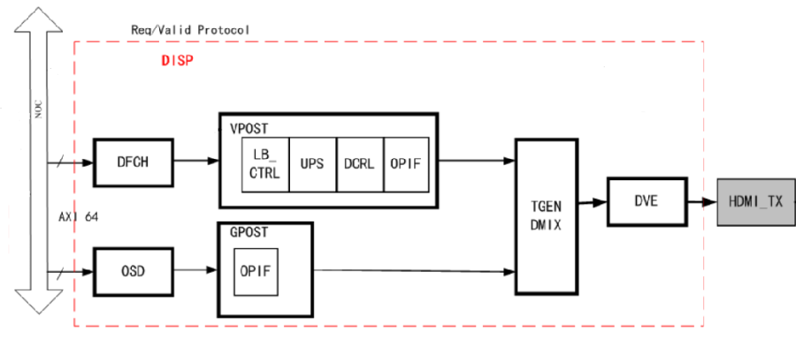
Figure 2021-1 Video Display Functional Blocks
- DFCH: Data fetch block, this block will de-interlace and fetch data from DRAM.
- VPOST: VPOST is simple version VPP which can translate data YUV422 to YUV444 and Frame crop and padding.
- OSD: OSD (On-Screen-Display) is the hardware providing bitmap display layer overlaying over or under other video and graphics display.
- GPOST: GPOST block is the wrapper for handling TGEN timing and Req/Valid junctions.
- DMIX: Display mixer(DMIX) supports mixing layers from OSD and VPP with display plane timing.
- TGEN: TGEN(Timing Generator) is mainly responsible for generating control timing for each module including field start, field end, field ID, display start pulse and pixel enable signal.
- DVE: DVE is a encode engine for two digital formats. One is HDMI, another is V656.
...
21.3 Data Input Source
The video display block data source has two, one is MIPI_CSI camera, another is USB camera. The data format include below list.
- Data from MIPI_CSI to DRAM, than data processed by CPU to produce Raw / YUV /RGB format.
- Data from MIPI_CSI to DRAM, than data don't processed by CPU and directly display Raw data.
- Data from USB camera, than data processed by CPU to produce Raw / YUV /RGB format.
...
21.4 DFCH (Data Fetch)
DFCH block also can be named DDFCH (De-interlace Data Fetch) due to its de-interlace function. The main function is fetched data from DRAM. There may be several types of data sources, and various formats are internally transmitted to the corresponding subsequent IP processing (VPOST). The features include below list.
...
The DDFCH functional block diagram is shown in figure 2021-2.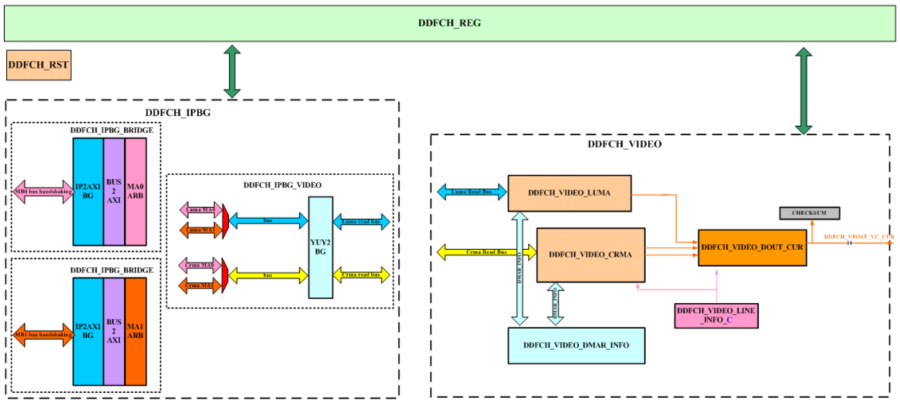
Figure 2021-2 DDFCH Functional Blocks
- DDFCH_RST: Protecting AXI-handshaking from Vsyn reset. When Vsync pulse raised, DDFCH_RST resets DDFCH until AXI-handshaking stop.
- DDFCH_REG: Handshaking with RGST Bus.
- DDFCH_IPBG: Arbitrating Motion and Video commands to AXI port 0 or port 1.
- DDFCH_IPBG_BRIDGE: For one AXI port, arbitrating Video commands.
- DDFCH_IPBG_VIDEO: Transforming video command to YUY2 mode and MUX commands to one AXI port.
- DDFCH_VIDEO: DMA-read current interlace source and reference interlace source for de-interlacing.
- DDFCH_VIDEO_LUMA: DMA-read Current luma source.
- DDFCH_VIDEO_CRMA: DMA-read Current chroma source.
- DDFCH_VIDEO_DOUT: Chroma-upsampling and VC-1 range-mapping Current pixels.
- DDFCH_VIDEO_DMAR_INFO: Calculating DMA-read info for Current luma and chroma data. It offers that line_start_addr info, vertical pre-decimation info and cropping info.
- DDFCH_VIDEO_LINE_INFO: Offer chroma-upsampleing line info.
...
21.5 VPOST (Video Post)
The VPOST block is kernel of video processor. It accepts two input sources, one is DMA input with YUV422 32bits format, another one is DDFCH input with YUV422 16bits format. This block will output data to DMIX block with YUV444 / Alpha 8 bits format. The VPOST functional block diagram is shown in figure 2021-3.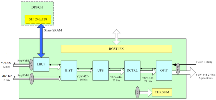
Figure 2021-3 VPOST Functional Blocks
- RGST IFX: This block will decode the control registers for VPOST.
- LBUF: LBUF block do line buffer to avoid DMA data less than real time. The SRAM is shared with DDFCH block.
- BIST: There are two functions in BIST block, they are Path Selection and Internal Pattern. The Path Selection can select input signal come from DMA or DDFCH, where the DMA data is 32 bits and must be converted to 16 bits.
- UPS: Chroma up sample 422 to 444.
- DCTRL: This block support cropping and padding. Once the original image is different from the resolution of the output image, the crop/padding function is used for output without scaling.
- OPIF: Interface between Req/Valid protocol and TGEN timing protocol.
...
21.6 OSD (On Screen Display)
OSD is the hardware providing bitmap display layer overlaying over or under other video and graphics display. This hardware is controlled by firmware through the register-file interface. If OSD enabled, it will read a linked-list data structure from the main-memory and output is sent to GSCL to scaling for compressing or directly display. Application may use this hardware to show user-interface message visually. The data support following color format.
...
The OSD functional block diagram is shown in figure 2021-4.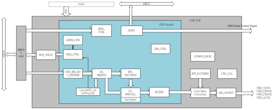
Figure 2021-4 OSD Functional Block
- RGST: This block will decode the control registers for OSD block
- HDR_CTRL: This block support header install and parser.
- ADDR_GEN: SBUS address generator.
- REQ_CTRL: SBUS request generator.
- DIS_CTRL: OSD timing generator.
- OSD_BM_RDY_DISTRIB: LB_BRIDGE pre-process.
- LB_BRIDGE: Line buffer bridge among LB/CP/BM_Decoder.
- BM_DECODER: This block supports bitmap decoder.
- CP_INSTALL: Color palette look up table install and index-color to direct-color transform.
- Line_buffer_xxx: Line buffer.
- SYSBUS_MON: Bus monitor.
- CRC_CAL: CRC checksum engine.
- INT_PATTERN: BIST internal pattern generator.
- Color Space Conversion: This block support color space conversion.
- BUS_WRAP: Generate pseudo MBUS grant to avoid critical path.
- DIS_OFFSET: Display offset block is frame base offset function.
...
21.7 GPOST
GPOST block is the wrapper for handling TGEN timing and Req/Valid junctions. It also provides Graph Path with simple image processing. The functions include below list.
- Contrast Adjustment
- Brightness Adjustment
- Hue and Saturation Adjustment
- Mask Function
...
21.8 DMIX
Display mixer(DMIX) supports mixing layers from OSD0~OSD3 and VPP0~VPP1 with display plane timing. DMIX output is to HD2SD/DVE. The main functions of DMIX are as below list.
...
The DMIX functional block diagram is shown in figure 2021-5.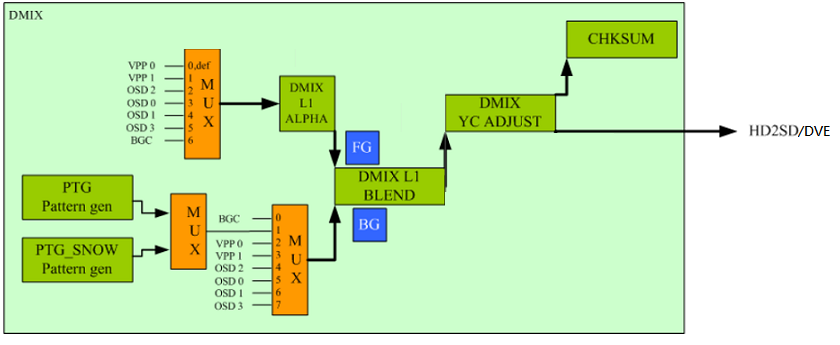
Figure 2021-5 DMIX Functional Block
- DMIX L1 ALPHA: This block is used to change the original alpha, the function can provide a fading effect.
- DMIX L1 BLEND: The blender is just to mix the foreground and background.
- DMIX YC ADJUST: This block is used for luma/chroma adjust.
- PTG: This pattern generator output internal color bar data.
- PTG_SNOW: This pattern generator output internal color snow data.
...
21.9 TGEN (Timing Generator)
TGEN(Timing Generator) is mainly responsible for generating of control timing for each module including field start, field end, field ID, display start pulse and pixel enable signal.
DTG, standing for Display Timing Generator, is the module that generates the control timing for modules dealing with display video formats. The Display Timing is generated according to the display video format. Display timing is the master timing of the whole system. If the display video format remains unchanged, display timing must be continuous. Even if the source video resolution changes, or if the configuration of display scaler changes.
The TGEN functional block diagram is shown in figure 2021-6.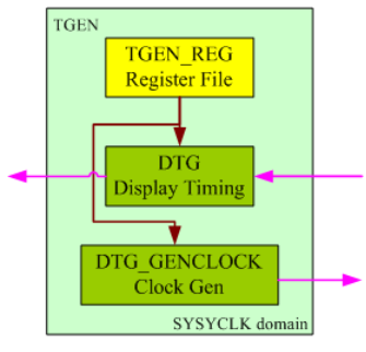
Figure 2021-6 TGEN Functional Block
...
21.10 DVE (Digital Video Encoder)
DVE(Digital Video Encoder) is a digital video encoder for HDMI Interfaces. The input data format is YUV444 and output data format is YUV444 36 bits with Separate Syncs.
Figure 2021-7 shows the DVE functional block diagram.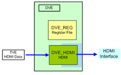
Figure 2021-7 DVE Functional Block
...
21.11 Registers Map
...
21.11.1 Registers Memory Map
De-interlace Data Fetch 0 (DDFCH0) Register Group
...
Address | Group No. | Register Name | Description |
|---|---|---|---|
0x9C007580 | G235.0 | Color bar mode | Color bar mode control |
0x9C007584 | G235.1 | Color bar V total | user mode V total |
0x9C007588 | G235.2 | Color bar V active | user mode V active |
0x9C00758C | G235.3 | Color bar V active start | user mode V active start |
0x9C007590 | G235.4 | Color bar H total | user mode H total |
0x9C007594 | G235.5 | Color bar H active | user mode H active |
0x9C007598 | G235.6 | DVE bit swap g0 | [BIT SW ON]bit swap group 0 |
0x9C00759C | G235.7 | DVE bit swap g1 | [BIT SW ON]bit swap group 1 |
0x9C0075A0 | G235.8 | DVE bit swap g2 | [BIT SW ON]bit swap group 2 |
0x9C0075A4 | G235.9 | DVE bit swap g3 | [BIT SW ON]bit swap group 3 |
0x9C0075A8 | G235.10 | DVE bit swap g4 | [BIT SW ON]bit swap group 4 |
0x9C0075AC | G235.11 | DVE bit swap g5 | [BIT SW ON]bit swap group 5 |
0x9C0075B0 | G235.12 | DVE bit swap g6 | [BIT SW ON]bit swap group 6 |
0x9C0075B4 | G235.13 | DVE bit swap g7 | [BIT SW ON]bit swap group 7 |
...
21.11.2 Registers Description
RGST Table Group 185 DDFCH0: De-interlace Data Fetch 0
185.0 DDFCH Latch Enable (ddfch0 latch en)
Address: 0x9C005C80
Reset: 0x0000 0001
...