21. DISPLAY
- edwin.chiu (Unlicensed)
- Michael Su (Unlicensed)
21.1 Introduction
The SP7021 video display function support video input source from camera, after data processed by CPU than output to HDMI. The video input can be MIPI_CSI or USB. SP7021 can support two channels MIPI_CSI camera. This module also supports directly raw data transfer to add efficiency. The Display Mixer function can mix one layer OSD and VPP data. The display output format support HDMI1.4 spec, HD resolution and YUV444 mode. The video display control registers locate at RGST Group 185~235 which memory map address are 0x9C005C80~0x9C0075FF.
21.2 Function Diagram
SP7021 video display function diagram is shown in Figure 21-1.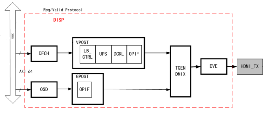
Figure 21-1 Video Display Functional Blocks
- DFCH: Data fetch block, this block will de-interlace and fetch data from DRAM.
- VPOST: VPOST is simple version VPP which can translate data YUV422 to YUV444 and Frame crop and padding.
- OSD: OSD (On-Screen-Display) is the hardware providing bitmap display layer overlaying over or under other video and graphics display.
- GPOST: GPOST block is the wrapper for handling TGEN timing and Req/Valid junctions.
- DMIX: Display mixer(DMIX) supports mixing layers from OSD and VPP with display plane timing.
- TGEN: TGEN(Timing Generator) is mainly responsible for generating control timing for each module including field start, field end, field ID, display start pulse and pixel enable signal.
- DVE: DVE is a encode engine for two digital formats. One is HDMI, another is V656.
21.3 Data Input Source
The video display block data source has two, one is MIPI_CSI camera, another is USB camera. The data format include below list.
- Data from MIPI_CSI to DRAM, than data processed by CPU to produce Raw / YUV /RGB format.
- Data from MIPI_CSI to DRAM, than data don't processed by CPU and directly display Raw data.
- Data from USB camera, than data processed by CPU to produce Raw / YUV /RGB format.
21.4 DFCH (Data Fetch)
DFCH block also can be named DDFCH (De-interlace Data Fetch) due to its de-interlace function. The main function is fetched data from DRAM. There may be several types of data sources, and various formats are internally transmitted to the corresponding subsequent IP processing (VPOST). The features include below list.
- Support AXI Protocol for command and data transfer.
- Video data source format supports YUV420, YUV422 and YUY2.
- Chroma upsample.
- Video data crop and decimation functions.
The DDFCH functional block diagram is shown in figure 21-2.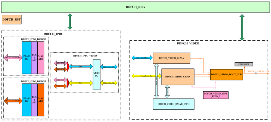
Figure 21-2 DDFCH Functional Blocks
- DDFCH_RST: Protecting AXI-handshaking from Vsyn reset. When Vsync pulse raised, DDFCH_RST resets DDFCH until AXI-handshaking stop.
- DDFCH_REG: Handshaking with RGST Bus.
- DDFCH_IPBG: Arbitrating Motion and Video commands to AXI port 0 or port 1.
- DDFCH_IPBG_BRIDGE: For one AXI port, arbitrating Video commands.
- DDFCH_IPBG_VIDEO: Transforming video command to YUY2 mode and MUX commands to one AXI port.
- DDFCH_VIDEO: DMA-read current interlace source and reference interlace source for de-interlacing.
- DDFCH_VIDEO_LUMA: DMA-read Current luma source.
- DDFCH_VIDEO_CRMA: DMA-read Current chroma source.
- DDFCH_VIDEO_DOUT: Chroma-upsampling and VC-1 range-mapping Current pixels.
- DDFCH_VIDEO_DMAR_INFO: Calculating DMA-read info for Current luma and chroma data. It offers that line_start_addr info, vertical pre-decimation info and cropping info.
- DDFCH_VIDEO_LINE_INFO: Offer chroma-upsampleing line info.
21.5 VPOST (Video Post)
The VPOST block is kernel of video processor. It accepts two input sources, one is DMA input with YUV422 32bits format, another one is DDFCH input with YUV422 16bits format. This block will output data to DMIX block with YUV444 / Alpha 8 bits format. The VPOST functional block diagram is shown in figure 21-3.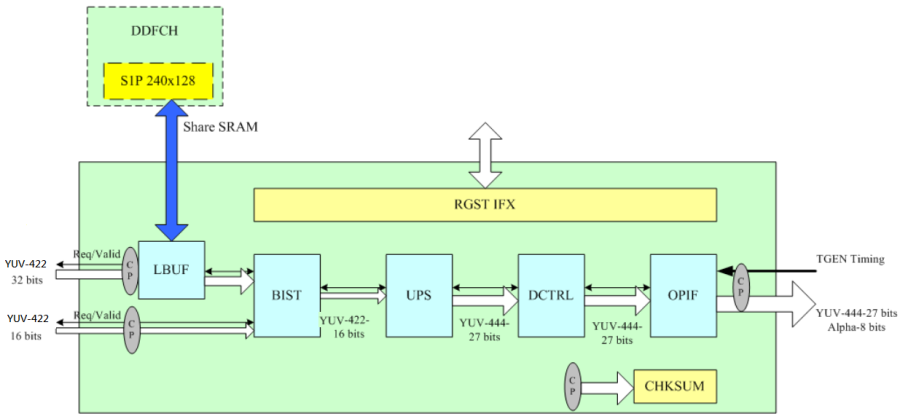
Figure 21-3 VPOST Functional Blocks
- RGST IFX: This block will decode the control registers for VPOST.
- LBUF: LBUF block do line buffer to avoid DMA data less than real time. The SRAM is shared with DDFCH block.
- BIST: There are two functions in BIST block, they are Path Selection and Internal Pattern. The Path Selection can select input signal come from DMA or DDFCH, where the DMA data is 32 bits and must be converted to 16 bits.
- UPS: Chroma up sample 422 to 444.
- DCTRL: This block support cropping and padding. Once the original image is different from the resolution of the output image, the crop/padding function is used for output without scaling.
- OPIF: Interface between Req/Valid protocol and TGEN timing protocol.
21.6 OSD (On Screen Display)
OSD is the hardware providing bitmap display layer overlaying over or under other video and graphics display. This hardware is controlled by firmware through the register-file interface. If OSD enabled, it will read a linked-list data structure from the main-memory and output is sent to GSCL to scaling for compressing or directly display. Application may use this hardware to show user-interface message visually. The data support following color format.
- 32-bit RGBA8888/ARGB8888
- 16-bit RGB565/ARGB1555/RGBA4444/ARGB4444/YUY2
- 8-bit color index mode with CLUT GBRA8888/YCbCrA8888/ARGB8888
The OSD functional block diagram is shown in figure 21-4.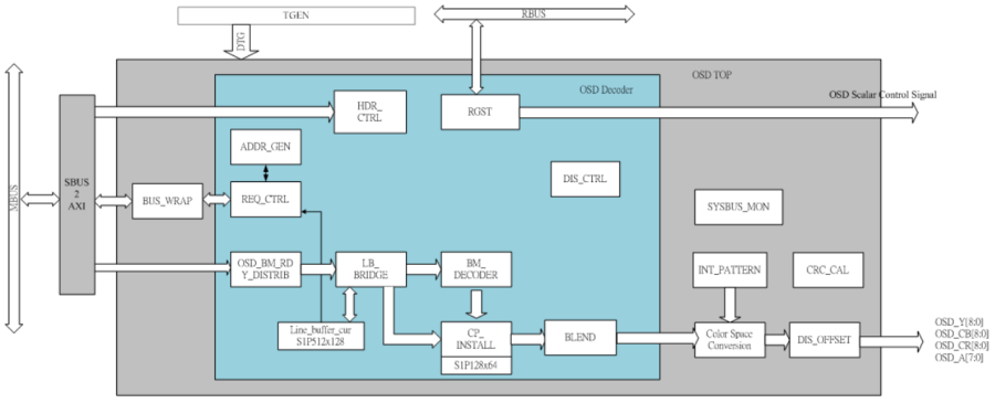
Figure 21-4 OSD Functional Block
- RGST: This block will decode the control registers for OSD block
- HDR_CTRL: This block support header install and parser.
- ADDR_GEN: SBUS address generator.
- REQ_CTRL: SBUS request generator.
- DIS_CTRL: OSD timing generator.
- OSD_BM_RDY_DISTRIB: LB_BRIDGE pre-process.
- LB_BRIDGE: Line buffer bridge among LB/CP/BM_Decoder.
- BM_DECODER: This block supports bitmap decoder.
- CP_INSTALL: Color palette look up table install and index-color to direct-color transform.
- Line_buffer_xxx: Line buffer.
- SYSBUS_MON: Bus monitor.
- CRC_CAL: CRC checksum engine.
- INT_PATTERN: BIST internal pattern generator.
- Color Space Conversion: This block support color space conversion.
- BUS_WRAP: Generate pseudo MBUS grant to avoid critical path.
- DIS_OFFSET: Display offset block is frame base offset function.
21.7 GPOST
GPOST block is the wrapper for handling TGEN timing and Req/Valid junctions. It also provides Graph Path with simple image processing. The functions include below list.
- Contrast Adjustment
- Brightness Adjustment
- Hue and Saturation Adjustment
- Mask Function
21.8 DMIX
Display mixer(DMIX) supports mixing layers from OSD0~OSD3 and VPP0~VPP1 with display plane timing. DMIX output is to HD2SD/DVE. The main functions of DMIX are as below list.
- Overlay
- Plane Alpha
- Blender
- All layers can be swap
- PTG (color bar with rotate function)
- Luma Adjustment (Constrast)
- Chroma Adjustment (Hue)
The DMIX functional block diagram is shown in figure 21-5.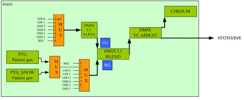
Figure 21-5 DMIX Functional Block
- DMIX L1 ALPHA: This block is used to change the original alpha, the function can provide a fading effect.
- DMIX L1 BLEND: The blender is just to mix the foreground and background.
- DMIX YC ADJUST: This block is used for luma/chroma adjust.
- PTG: This pattern generator output internal color bar data.
- PTG_SNOW: This pattern generator output internal color snow data.
21.9 TGEN (Timing Generator)
TGEN(Timing Generator) is mainly responsible for generating of control timing for each module including field start, field end, field ID, display start pulse and pixel enable signal.
DTG, standing for Display Timing Generator, is the module that generates the control timing for modules dealing with display video formats. The Display Timing is generated according to the display video format. Display timing is the master timing of the whole system. If the display video format remains unchanged, display timing must be continuous. Even if the source video resolution changes, or if the configuration of display scaler changes.
The TGEN functional block diagram is shown in figure 21-6.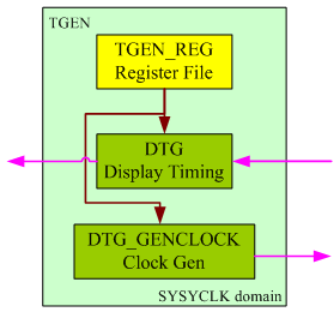
Figure 21-6 TGEN Functional Block
21.10 DVE (Digital Video Encoder)
DVE(Digital Video Encoder) is a digital video encoder for HDMI Interfaces. The input data format is YUV444 and output data format is YUV444 36 bits with Separate Syncs.
Figure 21-7 shows the DVE functional block diagram.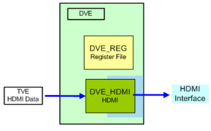
Figure 21-7 DVE Functional Block
21.11 Registers Map
21.11.1 Registers Memory Map
De-interlace Data Fetch 0 (DDFCH0) Register Group
Address | Group No. | Register Name | Description |
|---|---|---|---|
0x9C005C80 | G185.0 | ddfch0 latch en | DDFCH Latch Enable |
0x9C005C84 | G185.1 | ddfch0 mode option | Mode Option |
0x9C005C88 | G185.2 | ddfch0 enable | DDFCH Enable |
0x9C005C8C | G185.3 | ddfch0 urgent thd | DDFCH AXI Urgent Threshold |
0x9C005C90 | G185.4 | ddfch0 cmdq thd | DDFCH AXI Command Queue Threshold |
0x9C005C94 | G185.5 | G185ADDR5 | RESERVED |
0x9C005C98 | G185.6 | ddfch0 luma base addr 0 | Luma/YUY2 Base Address for Frame 0 |
0x9C005C9C | G185.7 | ddfch0 luma base addr 1 | Luma/YUY2 Base Address for Frame 1 |
0x9C005CA0 | G185.8 | ddfch0 luma base addr 2 | Luma/YUY2 Base Address for Frame 2 |
0x9C005CA4 | G185.9 | ddfch0 crma base addr 0 | Chroma Base Address for Frame 0 |
0x9C005CA8 | G185.10 | ddfch0 crma base addr 1 | Chroma Base Address for Frame 1 |
0x9C005CAC | G185.11 | ddfch0 crma base addr 2 | Chroma Base Address for Frame 2 |
0x9C005CB0 | G185.12 | G185ADDR12 | RESERVED |
0x9C005CB4 | G185.13 | G185ADDR13 | RESERVED |
0x9C005CB8 | G185.14 | G185ADDR14 | RESERVED |
0x9C005CBC | G185.15 | ddfch frame id | DDFCH Frame ID |
0x9C005CC0 | G185.16 | ddfch free run control | DDFCH Free-run Clock Control |
0x9C005CC4 | G185.17 | G185ADDR17 | RESERVED |
0x9C005CC8 | G185.18 | G185ADDR18 | RESERVED |
0x9C005CCC | G185.19 | G185ADDR19 | RESERVED |
0x9C005CD0 | G185.20 | ddfch0 vdo frame size | Line Pitch of Source in Video Frame Buffer |
0x9C005CD4 | G185.21 | ddfch0 vdo crop size | Video Crop Size |
0x9C005CD8 | G185.22 | ddfch0 vdo crop offset | Video Crop Offset |
0x9C005CDC | G185.23 | ddfch0 config 0 | Video Sideband Signal Config |
0x9C005CE0 | G185.24 | ddfch0 config 1 | Range Mapping Config |
0x9C005CE4 | G185.25 | G185ADDR25 | RESERVED |
0x9C005CE8 | G185.26 | ddfch0 chksum info | Check Sum |
0x9C005CEC | G185.27 | ddfch0 error flag info | DDFCH Error Flag |
0x9C005CF0 | G185.28 | ddfch0 bist | DDFCH BIST Mode and Output 422 YCbCr by Configuration |
0x9C005CF4 | G185.29 | ddfch0 axi ipbg info | DDFCH IPBG AXI Debug Information |
0x9C005CF8 | G185.30 | G185ADDR30 | RESERVED |
0x9C005CFC | G185.31 | ddfch0 others info | Others Debug Information |
On Screen Display Group0 (OSD0) Register Group 0
Address | Group No. | Register Name | Description |
|---|---|---|---|
0x9C006200 | G196.0 | osd ctrl | OSD Control Register |
0x9C006204 | G196.1 | osd en | OSD Enable |
0x9C006208 | G196.2 | osd base addr | OSD Base Address |
0x9C00620C | G196.3 | osd reserved 3 | OSD Reserved 3 |
0x9C006210 | G196.4 | osd reserved 4 | OSD Reserved 4 |
0x9C006214 | G196.5 | osd reserved 5 | OSD Reserved 5 |
0x9C006218 | G196.6 | osd bus monitor l | Debug register |
0x9C00621C | G196.7 | osd bus monitor h | Debug register |
0x9C006220 | G196.8 | osd req ctrl | OSD Request Control Register |
0x9C006224 | G196.9 | osd debug cmd lock | Debug register |
0x9C006228 | G196.10 | osd debug burst lock | Debug register |
0x9C00622C | G196.11 | osd debug xlen lock | Debug register |
0x9C006230 | G196.12 | osd debug ylen lock | Debug register |
0x9C006234 | G196.13 | osd debug queue lock | Debug register |
0x9C006238 | G196.14 | osd crc chksum | OSD field-updated CRC Checksum |
0x9C00623C | G196.15 | osd reserved 15 | OSD Reserved 15 |
0x9C006240 | G196.16 | osd hvld offset | Horizontal offset index |
0x9C006244 | G196.17 | osd hvld width | Horizon valid pixel number |
0x9C006248 | G196.18 | osd vvld offset | Vertical offset index |
0x9C00624C | G196.19 | osd vvld height | Vertical valid line nubmer |
0x9C006250 | G196.20 | osd data fetch ctrl | Memory Data Fetch Control |
0x9C006254 | G196.21 | osd bist ctrl | BIST Pattern |
0x9C006258 | G196.22 | osd non fetch 0 | OSD Non-fetching Region 0 |
0x9C00625C | G196.23 | osd non fetch 1 | OSD Non-fetching Region 1 |
0x9C006260 | G196.24 | osd non fetch 2 | OSD Non-fetching Region 2 |
0x9C006264 | G196.25 | osd non fetch 3 | OSD Non-fetching Region 3 |
0x9C006268 | G196.26 | osd bus status | Debug register |
0x9C00626C | G196.27 | osd 3d h offset | OSD 3D h offset |
0x9C006270 | G196.28 | osd reserved 28 | OSD Reserved 28 |
0x9C006274 | G196.29 | osd src decimation sel | SRC decimation selection |
0x9C006278 | G196.30 | osd bus time 0 | Debug register |
0x9C00627C | G196.31 | osd mbus time 1 | Debug register |
Video Post Processing (VPOST) Register Group
Address | Group No. | Register Name | Description |
|---|---|---|---|
0x9C006380 | G199.0 | ddfch0 latch en | DDFCH Latch Enable |
0x9C006384 | G199.1 | ddfch0 mode option | Mode Option |
0x9C006388 | G199.2 | ddfch0 enable | DDFCH Enable |
0x9C00638C | G199.3 | ddfch0 urgent thd | DDFCH AXI Urgent Threshold |
0x9C006390 | G199.4 | ddfch0 cmdq thd | DDFCH AXI Command Queue Threshold |
0x9C006394 | G199.5 | G185ADDR5 | RESERVED |
0x9C006398 | G199.6 | ddfch0 luma base addr 0 | Luma/YUY2 Base Address for Frame 0 |
0x9C00639C | G199.7 | ddfch0 luma base addr 1 | Luma/YUY2 Base Address for Frame 1 |
0x9C0063A0 | G199.8 | ddfch0 luma base addr 2 | Luma/YUY2 Base Address for Frame 2 |
0x9C0063A4 | G199.9 | ddfch0 crma base addr 0 | Chroma Base Address for Frame 0 |
0x9C0063A8 | G199.10 | ddfch0 crma base addr 1 | Chroma Base Address for Frame 1 |
0x9C0063AC | G199.11 | ddfch0 crma base addr 2 | Chroma Base Address for Frame 2 |
0x9C0063B0 | G199.12 | G185ADDR12 | RESERVED |
0x9C0063B4 | G199.13 | G185ADDR13 | RESERVED |
0x9C0063B8 | G199.14 | G185ADDR14 | RESERVED |
Graphic Post Processing (GPOST) Register Group 0
Address | Group No. | Register Name | Description |
|---|---|---|---|
0x9C006700 | G206.0 | gpost0 config | GPOST config register |
0x9C006704 | G206.1 | gpost0 mskl | Setting masked region |
0x9C006708 | G206.2 | gpost0 mskr | Setting masked region |
0x9C00670C | G206.3 | gpost0 mskt | Setting masked region |
0x9C006710 | G206.4 | gpost0 mskb | Setting masked region |
0x9C006714 | G206.5 | gpost0 bg1 | Background color YU |
0x9C006718 | G206.6 | gpost0 bg2 | Background color VA |
0x9C00671C | G206.7 | gpost0 contrast config | Contrast function enable |
0x9C006720 | G206.8 | gpost0 adj src | Contrast adjustment turning point |
0x9C006724 | G206.9 | gpost0 adj des | Contrast adjustment turning point |
0x9C006728 | G206.10 | gpost0 adj slope0 | Contrast adjustment slope |
0x9C00672C | G206.11 | gpost0 adj slope1 | Contrast adjustment slope |
0x9C006730 | G206.12 | gpost0 adj slope2 | GPOST Contrast adjustment slope |
0x9C006734 | G206.13 | gpost0 adj bound | Luma boundary value |
0x9C006738 | G206.14 | gpost0 bri value | Brightness value |
0x9C00673C | G206.15 | gpost0 hue sat en | Hue and saturation adjustment |
0x9C006740 | G206.16 | gpost0 chroma satsin | Chroma Adjust SATSIN Register |
0x9C006744 | G206.17 | gpost0 chroma satcos | Chroma Adjust SATCOS Register |
0x9C006748 | G206.18 | gpost0 master en | Master mode enable for setting start line and pixel of DMIX window |
0x9C00674C | G206.19 | gpost0 master horizontal | Setting start pixel of DMIX window |
0x9C006750 | G206.20 | gpost0 master vertical | Setting start line of DMIX window |
Timing Generator (TGEN) Register Group
Address | Group No. | Register Name | Description |
|---|---|---|---|
0x9C006A80 | G213.0 | tgen config | TGEN Config Register |
0x9C006A84 | G213.1 | tgen reset | TGEN Reset Register |
0x9C006A88 | G213.2 | user int1 config | User Interrupt 1 Config Register |
0x9C006A8C | G213.3 | user int2 config | User Interrupt 2 Config Register |
0x9C006A90 | G213.4 | dtg config | DTG Config Register |
0x9C006A94 | G213.5 | dtg clk conv thr | DTG colck conversion threshold |
0x9C006A98 | G213.6 | dtg delay field start lcnt | DTG delay field start linc count |
0x9C006A9C | G213.7 | dtg venc line rst cnt | DTG VENC Line Reset Control Register |
0x9C006AA0 | G213.8 | dtg total pixel | DTG Total Pixel Register |
0x9C006AA4 | G213.9 | dtg ds line start cd point | DTG DS LINE START CD Point Register |
0x9C006AA8 | G213.10 | dtg total line | DTG Total Line Register |
0x9C006AAC | G213.11 | dtg field end line | DTG Field End Line Register |
0x9C006AB0 | G213.12 | dtg start line | DTG ACTIVE START LINE |
0x9C006AB4 | G213.13 | dtg status1 | DTG Status Register 1 |
0x9C006AB8 | G213.14 | dtg status2 | DTG Status Register 2 |
0x9C006ABC | G213.15 | dtg status3 | DTG Status Register 3 |
0x9C006AC0 | G213.16 | dtg status4 | DTG Status Register 4dtg clk ratio |
0x9C006AC4 | G213.17 | dtg status5 | Reserved |
0x9C006AC8 | G213.18 | dtg clk ratio | DTG Clock Ratio |
0x9C006ACC | G213.19 | reserved | Reserved |
0x9C006AD0 | G213.20 | reserved | Reserved |
0x9C006AD4 | G213.21 | reserved | Reserved |
0x9C006AD8 | G213.22 | reserved | Reserved |
0x9C006ADC | G213.23 | dtg adjust1 | DTG Adjust Register 1 |
0x9C006AE0 | G213.24 | dtg adjust2 | DTG Adjust Register 2 |
0x9C006AE4 | G213.25 | dtg adjust3 | DTG Adjust Register 3 |
0x9C006AE8 | G213.26 | dtg adjust4 | DTG Adjust Register 4 |
0x9C006AEC | G213.27 | dtg adjust5 | DTG Adjust Register 5 |
0x9C006AF0 | G213.28 | reserved | Reserved |
0x9C006AF4 | G213.29 | source sel | Source select |
0x9C006AF8 | G213.30 | DTG FIELD START ADJ LCNT | Source select |
0x9C006AFC | G213.31 | reserved | Reserved |
Display Mixer 0 (DMIX0) Register Group
Address | Group No. | Register Name | Description |
|---|---|---|---|
0x9C006C80 | G217.0 | dmix config0 | DMIX Config Register 0 |
0x9C006C84 | G217.1 | dmix config1 | DMIX Config Register 1 |
0x9C006C88 | G217.2 | dmix config2 | DMIX Config Register 2 |
0x9C006C8C | G217.3 | dmix plane alpha | DMIX Plane Alpha Register |
0x9C006C90 | G217.4 | dmix plane alpha2 | DMIX Plane Alpha Register2 |
0x9C006C94 | G217.5 | dmix plane alpha3 | DMIX Plane Alpha Register3 |
0x9C006C98 | G217.6 | reserved | Reserved Register |
0x9C006C9C | G217.7 | dmix chksum | DMIX OUTPUT CHECK SUM |
0x9C006CA0 | G217.8 | dmix ptg config | DMIX PTG Config Register |
0x9C006CA4 | G217.9 | dmix ptg config2 | DMIX PTG Config Register |
0x9C006CA8 | G217.10 | dmix ptg config3 | DMIX PTG Config Register |
0x9C006CAC | G217.11 | dmix ptg config4 | DMIX PTG Config Register |
0x9C006CB0 | G217.12 | dmix ptg config5 | DMIX PTG Config Register |
0x9C006CB4 | G217.13 | dmix ptg config6 | DMIX PTG Config Register |
0x9C006CB8 | G217.14 | reserved | Reserved Register |
0x9C006CBC | G217.15 | reserved | Reserved Register |
0x9C006CC0 | G217.16 | dmix yc adjust | DMIX YC Adjust Register |
0x9C006CC4 | G217.17 | dmix luma cp1 | DMIX Luma Adjust Control Point 1 Register |
0x9C006CC8 | G217.18 | dmix luma cp2 | DMIX Luma Adjust Control Point 2 Register |
0x9C006CCC | G217.19 | dmix luma cp3 | DMIX Luma Adjust Control Point 3 Register |
0x9C006CD0 | G217.20 | dmix luma slope0 | DMIX Luma Adjust Slope 0 Register |
0x9C006CD4 | G217.21 | dmix luma slope1 | DMIX Luma Adjust Slope 1 Register |
0x9C006CD8 | G217.22 | dmix luma slope2 | DMIX Luma Adjust Slope 2 Register |
0x9C006CDC | G217.23 | dmix luma slope3 | DMIX Luma Adjust Slope 3 Register |
0x9C006CE0 | G217.24 | dmix chroma satcos | DMIX Chroma Adjust SATCOS Register |
0x9C006CE4 | G217.25 | dmix chroma satsin | DMIX Chroma Adjust SATSIN Register |
0x9C006CE8 | G217.26 | dmix pix en sel | DMIX PIX EN SEL |
0x9C006CEC | G217.27 | reserved | Reserved Register |
0x9C006CF0 | G217.28 | reserved | Reserved |
0x9C006CF4 | G217.29 | reserved | Reserved Register |
0x9C006CF8 | G217.30 | reserved | Reserved Register |
0x9C006CFC | G217.31 | reserved | Reserved |
Video Encoder (DVE) Register Group 0
Address | Group No. | Register Name | Description |
|---|---|---|---|
0x9C007500 | G234.0 | dve vsync start top | Top v-sync start by HDMI User Mode |
0x9C007504 | G234.1 | dve vsync start bot | Bottom v-sync start by HDMI User Mode |
0x9C007508 | G234.2 | dve vsync h point | V-sync status toggle at horizontal point by HDMI User Mode |
0x9C00750C | G234.3 | dve vsync pd cnt | V-sync witch line by HDMI User Mode |
0x9C007510 | G234.4 | dve hsync start | H-sync start by HDMI User Mode |
0x9C007514 | G234.5 | dve hsync pd cnt | H-sync witch pixel by HDMI User Mode |
0x9C007518 | G234.6 | dve hdmi mode 1 | HDMI Mode 1 Control |
0x9C00751C | G234.7 | dve v vld top start | Top vertical valid start by HDMI User Mode |
0x9C007520 | G234.8 | dve v vld top end | Top vertical valid end by HDMI User Mode |
0x9C007524 | G234.9 | dve v vld bot start | Bottom vertical valid start by HDMI User Mode |
0x9C007528 | G234.10 | dve v vld bot end | Bottom vertical valid end by HDMI User Mode |
0x9C00752C | G234.11 | dve de h start | Data enable horizontal start by HDMI User Mode |
0x9C007530 | G234.12 | dve de h end | Data enable horizontal end by HDMI User Mode |
0x9C007534 | G234.13 | dve mp tg line 0 length | Total pixel by HDMI User Mode |
0x9C007538 | G234.14 | dve mp tg frame 0 line | Total line by HDMI User Mode |
0x9C00753C | G234.15 | dve mp tg act 0 pix | Active pixel by HDMI User Mode |
0x9C007540 | G234.16 | dve hdmi mode 0 | HDMI Mode Control |
0x9C007544 | G234.17 | dve act 0 pix 656 | Active pixel by CCIR656 User Mode |
0x9C007548 | G234.18 | dve line 0 length 656 | Line pixel length by CCIR656 User Mode |
0x9C00754C | G234.19 | dve frame 0 line 656 | Active line number by CCIR656 User Mode |
0x9C007550 | G234.20 | dve noact end tl 656 | TOP blanking line end by CCIR656 User Mode |
0x9C007554 | G234.21 | dve act end tl 656 | TOP active line end by CCIR656 User Mode |
0x9C007558 | G234.22 | dve noact end bl 656 | Bottom blanking line end by CCIR656 User Mode |
0x9C00755C | G234.23 | dve act end bl 656 | Bottom active line end by CCIR656 User Mode |
0x9C007560 | G234.24 | dve ccir656 ctrl 0 | CCIR656 Control |
0x9C007564 | G234.25 | dve d656 y range | Value limiter of Luma |
0x9C007568 | G234.26 | dve d656 c range | Value limiter of Chroma |
0x9C00756C | G234.27 | reserved | |
0x9C007570 | G234.28 | reserved | |
0x9C007574 | G234.29 | dve hdmi sharp | Sharpness control for HDMI |
0x9C007578 | G234.30 | dve config1 | DVE Config1 Register |
0x9C00757C | G234.31 | dve checksum | DVE checksum |
Video Encoder (DVE) Register Group 1
Address | Group No. | Register Name | Description |
|---|---|---|---|
0x9C007580 | G235.0 | Color bar mode | Color bar mode control |
0x9C007584 | G235.1 | Color bar V total | user mode V total |
0x9C007588 | G235.2 | Color bar V active | user mode V active |
0x9C00758C | G235.3 | Color bar V active start | user mode V active start |
0x9C007590 | G235.4 | Color bar H total | user mode H total |
0x9C007594 | G235.5 | Color bar H active | user mode H active |
0x9C007598 | G235.6 | DVE bit swap g0 | [BIT SW ON]bit swap group 0 |
0x9C00759C | G235.7 | DVE bit swap g1 | [BIT SW ON]bit swap group 1 |
0x9C0075A0 | G235.8 | DVE bit swap g2 | [BIT SW ON]bit swap group 2 |
0x9C0075A4 | G235.9 | DVE bit swap g3 | [BIT SW ON]bit swap group 3 |
0x9C0075A8 | G235.10 | DVE bit swap g4 | [BIT SW ON]bit swap group 4 |
0x9C0075AC | G235.11 | DVE bit swap g5 | [BIT SW ON]bit swap group 5 |
0x9C0075B0 | G235.12 | DVE bit swap g6 | [BIT SW ON]bit swap group 6 |
0x9C0075B4 | G235.13 | DVE bit swap g7 | [BIT SW ON]bit swap group 7 |
21.11.2 Registers Description
RGST Table Group 185 DDFCH0: De-interlace Data Fetch 0
185.0 DDFCH Latch Enable (ddfch0 latch en)
Address: 0x9C005C80
Reset: 0x0000 0001
| Field Name | Bit | Access | Description |
| G185A0 Reserved0 | 31:1 | DC | RESERVED |
| atch en | 0 | RW | latch enable 0: direct mode 1: latch mode (default) |
185.1 Mode Option (ddfch0 mode option)
Address: 0x9C005C84
Reset: 0x0001 E000
| Field Name | Bit | Access | Description |
| G185A1 Reserved4 | 31:22 | DC | RESERVED |
| H265 EN | 21 | RW | DDFCH DRAM source is H265 0: source is NOT H265 (default) 1: source is H265 When DRAM source is H265, DRAM buffer is field base, otherwise buffer is frame base. |
| G185A1 Reserved3 | 20:19 | DC | RESERVED |
| chroma arb to axi | 18 | RW | chroma axi command go to axi port MA0 or MA1 0: MA0 (default) 1: MA1 |
| luma arb to axi | 17 | RW | luma axi command go to axi port MA0 or MA1 0: MA0 (default) 1: MA1 |
| G185A1 Reserved2 | 16:15 | DC | RESERVED |
| chroma irbg en | 14 | RW | chroma axi command A16B16 to A32B32 bridge enable 0: disable 1: enable (default) |
luma irbg en | 13 | RW | luma axi command A16B16 to A32B32 bridge enable |
G185A1 Reserved1 | 12 | DC | RESERVED |
yuy2 en | 11 | RW | previous/current/next data fetch yuy2 mode enable |
src 422 c | 10 | RW | source content option of current field data fetch (merge C/P/N) |
G185A1 Reserved0 | 9:0 | DC | RESERVED |
185.2 DDFCH Enable (ddfch0 enable)
Address: 0x9C005C88
Reset: 0x0000 00E0
Field Name | Bit | Access | Description |
G185A2 Reserved2 | 31:8 | DC | RESERVED |
c ug en | 7 | RW | video chroma axi urgent enable |
l ug en | 6 | RW | video luma axi urgent enable |
G185A2 Reserved1 | 5 | DC | RESERVED |
cu en | 4 | RW | current data fetch enable |
G185A2 Reserved0 | 3:0 | DC | RESERVED |
185.3 DDFCH AXI Urgent Threshold (ddfch0 urgent thd)
Address: 0x9C005C8C
Reset: 0x00D6 D6D6
Field Name | Bit | Access | Description |
| G185A3 Reserved1 | 31:24 | DC | RESERVED |
| c ug thd | 23:16 | RW | video chroma axi urgent threshold 0~240: when buffer > threshold, urgent flag will become high. |
| l ug thd | 15:8 | RW | video luma axi urgent threshold 0~240: when buffer > threshold, urgent flag will become high. |
| G185A3 Reserved0 | 7:0 | DC | RESERVED |
185.4 DDFCH AXI Command Queue Threshold (ddfch0 cmdq thd)
Address: 0x9C005C90
Reset: 0x0000 00FF
Field Name | Bit | Access | Description |
| G185A4 Reserved0 | 31:8 | DC | RESERVED |
| c cmdq thd | 7:4 | RW | video chroma axi command queue threshold it must be >= 1 |
| l cmdq thd | 3:0 | RW | video luma axi command queue threshold it must be >= 1 |
185.5 RESERVED (G185ADDR5)
Address: 0x9C005C94
Reset: 0x0
Field Name | Bit | Access | Description |
| G185A5 Reserved0 | 31:0 | DC | RESERVED |
185.6 Luma/YUY2 Base Address for Frame 0 (ddfch0 luma base addr 0)
Address: 0x9C005C98
Reset: 0x0
Field Name | Bit | Access | Description |
| G185A6 Reserved0 | 31:22 | DC | RESERVED |
| luma base addr 0 | 21:0 | RW | luma/yuy2 base addr for frame 0 this register supports: [1] yuy2 mode base address, unit is K-byte [2] Previous field base address when H265 EN ON, unit is K-byte [3] Frame base address when H265 EN OFF, unit is K-byte |
185.7 Luma/YUY2 Base Address for Frame 1 (ddfch0 luma base addr 1)
Address: 0x9C005C9C
Reset: 0x0
Field Name | Bit | Access | Description |
| G185A7 Reserved0 | 31:22 | DC | RESERVED |
| luma base addr 1 | 21:0 | RW | luma/yuy2 base addr for frame 1 this register supports: [1] yuy2 mode base address, unit is K-byte [2] Current field base address when H265 EN ON, unit is K-byte [3] Frame base address when H265 EN OFF, unit is K-byte |
185.8 Luma/YUY2 Base Address for Frame 2 (ddfch0 luma base addr 2)
Address: 0x9C005CA0
Reset: 0x0
Field Name | Bit | Access | Description |
| G185A8 Reserved0 | 31:22 | DC | RESERVED |
| luma base addr 2 | 21:0 | RW | luma/yuy2 base addr for frame 2 this register supports: [1] yuy2 mode base address, unit is K-byte [2] Next field base address when H265 EN ON, unit is K-byte [3] Frame base address when H265 EN OFF, unit is K-byte |
185.9 Chroma Base Address for Frame 0 (ddfch0 crma base addr 0)
Address: 0x9C005CA4
Reset: 0x0
Field Name | Bit | Access | Description |
| G185A9 Reserved0 | 31:22 | DC | RESERVED |
| crma base addr 0 | 21:0 | RW | chroma base addr for frame 0 this register supports: [1] Previous field base address when H265 EN ON, unit is K-byte [2] Frame base address when H265 EN OFF, unit is K-byte |
185.10 Chroma Base Address for Frame 1 (ddfch0 crma base addr 1)
Address: 0x9C005CA8
Reset: 0x0
Field Name | Bit | Access | Description |
| G185A10 Reserved0 | 31:22 | DC | RESERVED |
| crma base addr 1 | 21:0 | RW | chroma base addr for frame 1 this register supports: [1] Current field base address when H265 EN ON, unit is K-byte [2] Frame base address when H265 EN OFF, unit is K-byte |
185.11 Chroma Base Address for Frame 2 (ddfch0 crma base addr 2)
Address: 0x9C005CAC
Reset: 0x0
Field Name | Bit | Access | Description |
| G185A11 Reserved0 | 31:22 | DC | RESERVED |
| crma base addr 2 | 21:0 | RW | chroma base addr for frame 2 This register supports: [1] Next field base address when H265 EN ON, unit is K-byte [2] Frame base address when H265 EN OFF, unit is K-byte |
185.12 RESERVED (G185ADDR12)
Address: 0x9C005CB0
Reset: 0x0
Field Name | Bit | Access | Description |
| G185A12 Reserved0 | 31:0 | DC | RESERVED |
185.13 RESERVED (G185ADDR13)
Address: 0x9C005CB4
Reset: 0x0
Field Name | Bit | Access | Description |
| G185A13 Reserved0 | 31:0 | DC | RESERVED |
185.14 RESERVED (G185ADDR14)
Address: 0x9C005CB8
Reset: 0x0
Field Name | Bit | Access | Description |
| G185A14 Reserved0 | 31:0 | DC | RESERVED |
185.15 DDFCH Frame ID (ddfch frame id)
Address: 0x9C005CBC
Reset: 0x0
Field Name | Bit | Access | Description |
| G185A15 Reserved1 | 31:6 | DC | RESERVED |
| frm id c | 5:4 | RW | current field base on which frame others: frame 2 |
| G185A15 Reserved0 | 3:0 | DC | RESERVED |
185.16 DDFCH Free-run Clock Control (ddfch free run control)
Address: 0x9C005CC0
Reset: 0x0
Field Name | Bit | Access | Description |
| G185A16 Reserved1 | 31:7 | DC | RESERVED |
| GCLK DDFCH0 IPBG | 6 | RW | clock free-run or gating clock(power saving) 0:gating clock(power saving)(default) 1:free-run |
| GCLK DDFCH0 INFO | 5 | RW | clock free-run or gating clock(power saving) 0:gating clock(power saving)(default) 1:free-run |
| GCLK DDFCH0 CRMA | 4 | RW | clock free-run or gating clock(power saving) 0:gating clock(power saving)(default) 1:free-run |
| GCLK DDFCH0 LUMA | 3 | RW | RW clock free-run or gating clock(power saving) 0:gating clock(power saving)(default) 1:free-run |
| G185A16 Reserved0 | 2:1 | DC | RESERVED |
| GCLK DDFCH0 REG | 0 | RW | clock free-run or gating clock(power saving) 0:gating clock(power saving)(default) 1:free-run |
185.17 RESERVED (G185ADDR17)
Address: 0x9C005CC4
Reset: 0x0
Field Name | Bit | Access | Description |
| G185A17 Reserved0 | 31:0 | DC | RESERVED |
185.18 RESERVED (G185ADDR18)
Address: 0x9C005CC8
Reset: 0x0
Field Name | Bit | Access | Description |
| G185A18 Reserved0 | 31:0 | DC | RESERVED |
185.19 RESERVED (G185ADDR19)
Address: 0x9C005CCC
Reset: 0x0
Field Name | Bit | Access | Description |
| G185A19 Reserved0 | 31:0 | DC | RESERVED |
185.20 Line Pitch of Source in Video Frame Buffer (ddfch0 vdo frame size)
Address: 0x9C005CD0
Reset: 0x0
Field Name | Bit | Access | Description |
| G185A20 Reserved0 | 31:13 | DC | RESERVED |
| vdo f size | 12:0 | RW | line pitch of source in video frame buffer unit is byte EX: 8-bit per pixs, 720x480, if x size = 720, vdo f size = 768 (a little bigger than x size and align 128) |
185.21 Video Crop Size (ddfch0 vdo crop size)
Address: 0x9C005CD4
Reset: 0x0
Field Name | Bit | Access | Description |
G185A21 Reserved1 | 31:28 | DC | RESERVED |
vdo y size | 27:16 | RW | video crop line size |
G185A21 Reserved0 | 15:13 | DC | RESERVED |
| vdo x size | 12:0 | RW | video crop pixel size unit is byte 8 bit per pix, cropping and no HDCM : x size aligned 2 cropping and HDCM by2 : x size aligned 16 cropping and HDCM by4 : x size aligned 32 |
185.22 Video Crop Offset (ddfch0 vdo crop offset)
Address: 0x9C005CD8
Reset: 0x0
Field Name | Bit | Access | Description |
| G185A22 Reserved1 | 31:28 | DC | RESERVED |
| vdo y st | 27:16 | RW | video crop line start y st aligned 2 |
| G185A22 Reserved0 | 15:13 | DC | RESERVED |
| vdo x st | 12:0 | RW | video crop pixel start 8 bit per pix, cropping start from (x st, y st) = (0, 0) cropping and no HDCM : x st aligned 16 cropping and HDCM by2 : x st aligned 32 cropping and HDCM by4 : x st aligned 64 |
185.23 Video Sideband Signal Config (ddfch0 config 0)
Address: 0x9C005CDC
Reset: 0x0001 0000
Field Name | Bit | Access | Description |
| G185A23 Reserved5 | 31:30 | DC | RESERVED |
| cur y st shift | 29 | RW | For the case that chroma upsample at frame mode but output top/bottom field Note that y st shift is valid only at the case that frame mode and STEP=2 |
| G185A23 Reserved4 | 28:27 | DC | RESERVED |
crma repeat | 26 | RW | using chroma line repeat to upsample 420 to 422 of cur- rent field data fetch (merge C/P/N) |
G185A23 Reserved3 | 25:18 | DC | RESERVED |
step | 17:16 | RW | current data vertical decimation (merge C/P/N) |
G185A23 Reserved2 | 15:12 | DC | RESERVED |
dcm mode | 11 | RW | current data horizontal decimation mode (merge C/P/N) |
dcm en | 10 | RW | current data horizontal decimation enable (merge |
G185A23 Reserved1 | 9:6 | DC | RESERVED |
fid c | 5 | RW | current data fetch field id |
il c | 4 | RW | current data fetch frame/field |
G185A23 Reserved0 | 3:0 | DC | RESERVED |
185.24 Range Mapping Config (ddfch0 config 1)
Address: 0x9C005CE0
Reset: 0x0
Field Name | Bit | Access | Description |
| G185A24 Reserved4 | 31 | DC | RESERVED |
cu rm en c | 30 | RW | current data fetch chroma range map enable |
G185A24 Reserved3 | 29:27 | DC | RESERVED |
cu rm en l | 26 | RW | current data fetch luma range map enable |
G185A24 Reserved2 | 25:23 | DC | RESERVED |
cu rm c | 22:20 | RW | current data fetch chroma range map parameter |
G185A24 Reserved1 | 19:11 | DC | RESERVED |
cu rm l | 10:8 | RW | current data fetch luma range map parameter |
G185A24 Reserved0 | 7:0 | DC | RESERVED |
185.25 RESERVED (G185ADDR25)
Address: 0x9C005CE4
Reset: 0x0
Field Name | Bit | Access | Description |
| G185A25 Reserved0 | 31:0 | DC | RESERVED |
185.26 Check Sum (ddfch0 chksum info)
Address: 0x9C005CE8
Reset: 0x0
Field Name | Bit | Access | Description |
| G185A26 Reserved0 | 31:16 | DC | RESERVED |
| check sum | 15:0 | RO | check sum Always monitor CUR engine. |
185.27 DDFCH Error Flag (ddfch0 error flag info)
Address: 0x9C005CEC
Reset: 0x0
Field Name | Bit | Access | Description |
| G185A27 Reserved4 | 31:18 | DC | RESERVED |
| axi rresp ma1 status | 17:16 | RO | latch AXI read response error status in MA1 RGST write command: 0x1: clean error status others: reserved. RGST read command: 0x0 means OKAY. 0x1 means EXOKAY. 0x2 means SLVERR. 0x3 means DECERR. |
| G185A27 Reserved3 | 15:14 | DC | RESERVED |
| axi rresp ma0 status | 13:12 | RO | latch AXI read response error status in MA0 RGST write command: 0x1: clean error status others: reserved. RGST read command: 0x0 means OKAY. 0x1 means EXOKAY. 0x2 means SLVERR. 0x3 means DECERR. |
| G185A27 Reserved2 | 11 | DC | RESERVED |
| burst cnt ma1 error flag | 10 | OTHER | when axi MA1 doesnt have 32 bursts per cmd, error flag=1 RGST write command: 0: DO NOT clean error flag 1: clean error flag RGST read command: 0: error flag is NOT valid 1: error flag valid |
| burst cnt ma0 error flag | 9 | OTHER | when axi MA0 doesnt have 32 bursts per cmd, error flag=1 RGST write command: 0: DO NOT clean error flag 1: clean error flag RGST read command: 0: error flag is NOT valid 1: error flag valid |
| cur luma lb empty flag | 8 | OTHER | current luma line buffer empty in active line RGST write command: 0: DO NOT clean error flag 1: clean error flag RGST read command: 0: error flag is NOT valid 1: error flag valid |
| G185A27 Reserved1 | 7:6 | RO | RESERVED |
| cu er flag | 5 | OTHER | current luma data fetch incomplete frame RGST write command: 0: DO NOT clean error flag 1: clean error flag RGST read command: 0: error flag is NOT valid 1: error flag valid |
| G185A27 Reserved0 | 4:0 | DC | RESERVED |
185.28 DDFCH BIST Mode andOutput 422 YCbCr by Configuration (ddfch0 bist)
Address: 0x9C005CF0
Reset: 0x0
Field Name | Bit | Access | Description |
| bist cr | 31:24 | RW | bist mode background color chroma element Cr |
| bist cb | 23:16 | RW | bist mode background color chroma element Cb |
| bist y | 15:8 | RW | bist mode background color luma element Y |
| G185A28 Reserved | 17:6 | DC | RESERVED |
| bist pattern mode | 5:4 | RW | bist pattern mode According to video size |
| G185A28 Reserved0 | 3:2 | DC | RESERVED |
| bist pattern type | 1 | RW | bist mode pattern type CUR engine bist output data volume. |
| bist en | 0 | RW | bist mode enable 0: off (Disable) (default) 1: on |
185.29 DDFCH IPBG AXI Debug Information (ddfch0 axi ipbg info)
Address: 0x9C005CF4
Reset: 0x0
Field Name | Bit | Access | Description |
| G185A29 Reserved2 | 31:24 | DC | RESERVED |
| cnt aw cp depth ma1 | 23:22 | RO | monitor write cmd fifo in MA1 it should be zero at filed end |
| cnt ar cp depth ma1 | 21:20 | RO | monitor read cmd fifo in MA1 it should be zero at filed end |
| cnt aw cp depth ma0 | 19:18 | RO | monitor write cmd fifo in MA0 it should be zero at filed end |
| cnt ar cp depth ma0 | 17:16 | RO | monitor read cmd fifo in MA0 it should be zero at filed end |
| G185A29 Reserved1 | 15:13 | DC | RESERVED |
| arb cmdq num ma1 | 12:8 | RO | the residual command which axi port 1 didn't get yet it should be zero at filed end |
G185A29 Reserved0 | 7:5 | DC | RESERVED |
arb cmdq num ma0 | 4:0 | RO | the residual command which axi port 0 didn't get yet it should be zero at filed end |
185.30 RESERVED (G185ADDR30)
Address: 0x9C005CF8
Reset: 0x0
Field Name | Bit | Access | Description |
| G185A30 Reserved1 | 31:0 | DC | RESERVED |
185.31 Others Debug Information (ddfch0 others info)
Address: 0x9C005CFC
Reset: 0x0
Field Name | Bit | Access | Description |
| G185A31 Reserved1 | 31:20 | DC | RESERVED |
| MONITOR START LINE | 19:8 | RW | CUR luma line buffer monitor start line(when AXI ac- cept cmd), to monitor line buffer empty error use in error flag, G185.27[8] |
| G185A31 Reserved0 | 7:2 | DC | RESERVED |
| DDFCH VPOST CUR VALID | 1 | RO | monitor between DDFCH and VPOST CUR interface from DDFCH to VPOST |
| VPOST DDFCH CUR REQ | 0 | RO | monitor between DDFCH and VPOST CUR interface |
RGST Table Group 196 OSD0 G0
196.0 OSD Control Register (osd ctrl)
Address: 0x9C006200
Reset: 0x0000 0027
Field Name | Bit | Access | Description |
| reserved | 31:16 | RO | RESERVED |
| reserved | 15:13 | RW | RESERVED |
| OSD FLAG CLEAN | 12 | RW | OSD error flag cleaning This function can be switched on by changing polarity of this bit |
| reserved | 11 | RW | RESERVED |
| OSD COLOR RGB | 10 | RW | select output transparent RGB value 0: YUV Black Color. (default) 1: RGB Black Color. |
| reserved | 9 | RW | RESERVED |
| OSD NON FETCH EN | 8 | RW | Enable non-fetching region 0: Disable (default) 1: Enable |
| OSD CLUT FORMAT SEL | 7 | RW | CLUT format selection 0: YCbCrA8888/GBRA8888 (default) 1: ACrYCb8888/ARGB8888 |
| reserved | 6 | RW | RESERVED |
| OSD latch en | 5 | RW | updates configure only at field start 0: off(direct mode) 1: on(latch mode) (default) Note: Not support danamic switch. |
| OSD A32B32 EN | 4 | RW | Enable A32B32 fetching 0: Disable (A16B16)(default) 1: Enable (A32B32) |
| reserved | 3 | RW | RESERVED |
| REQ FIFO DEPTH | 2:0 | RW | Request fifo depth for DRAM request, 0: Not allowed 1 7: Allowed range for request fifo depth |
196.1 OSD Enable (osd en)
Address: 0x9C006204
Reset: 0x0
Field Name | Bit | Access | Description |
| reserved | 31:13 | RO | RESERVED |
| GCLK FORCE FREE | 12:4 | RW | Force gated clock to free run clock bit 05: For GCLK OSD DEHEADER G2 bit 06: For GCLK OSD DEHEADER G3 bit 07: For GCLK OSD DEHEADER G4 bit 08: For GCLK OSD DEHEADER G5 bit 09: For GCLK OSD DEHEADER G6 bit 10: For GCLK OSD DEHEADER G7 bit 11: For GCLK OSD DEHEADER G8 bit 12: For GCLK OSD DEHEADER G9 |
| reserved | 3:1 | RO | RESERVED |
| OSD en | 0 | RW | enable of OSD function 0: Disable (default) 1: Enable |
196.2 OSD Base Address (osd base addr)
Address: 0x9C006208
Reset: 0xFFFF FFE0
Field Name | Bit | Access | Description |
| OSD BASE ADDR | 31:5 | RW | Link pointer to the first display region. |
| reserved | 4:0 | RO | RESERVED |
196.3 OSD Reserved 3 (osd reserved 3)
Address: 0x9C00620C
Reset: 0x0
Field Name | Bit | Access | Description |
| reserved | 31:0 | RO | RESERVED |
196.4 OSD Reserved 4 (osd reserved 4)
Address: 0x9C006210
Reset: 0x0
Field Name | Bit | Access | Description |
| reserved | 31:0 | RO | RESERVED |
196.5 OSD Reserved 5 (osd reserved 5)
Address: 0x9C006214
Reset: 0x0
Field Name | Bit | Access | Description |
| reserved | 31:0 | RO | RESERVED |
196.6 Debug register (reserved)
Address: 0x9C006218
Reset: 0x0
Field Name | Bit | Access | Description |
| reserved | 31:0 | RO | RESERVED |
196.7 Debug register (reserved)
Address: 0x9C00621C
Reset: 0x0
Field Name | Bit | Access | Description |
| reserved | 31:0 | RO | RESERVED |
196.8 OSD Request Control Register (osd req ctrl)
Address: 0x9C006220
Reset: 0x0000 8020
Field Name | Bit | Access | Description |
| reserved | 31:16 | RO | RESERVED |
| OSD urg regu en | 15 | RW | osd vblank urgent regulator function enable |
| reserved | 14:9 | RO | RESERVED |
| OSD urg th | 8:0 | RW | osd fifo urgent threshold 0x1FF..0x100: always urgent 0x0: no urgent request other: urgent when the fifo-grant-count smaller than this value unit: 32bytes, bit[1:0] will be discarded |
196.9 Debug register (reserved)
Address: 0x9C006224
Reset: 0x0
Field Name | Bit | Access | Description |
| reserved | 31:16 | RO | RESERVED |
reserved | 15:0 | RW | RESERVED |
196.10 Debug register (reserved)
Address: 0x9C006228
Reset: 0x0
Field Name | Bit | Access | Description |
| reserved | 31:6 | RO | RESERVED |
| reserved | 5:0 | RW | RESERVED |
196.11 Debug register (reserved)
Address: 0x9C00622C
Reset: 0x0
Field Name | Bit | Access | Description |
| reserved | 31:13 | RO | RESERVED |
| reserved | 12:0 | RW | RESERVED |
196.12 Debug register (reserved)
Address: 0x9C006230
Reset: 0x0
Field Name | Bit | Access | Description |
| reserved | 31:12 | RO | RESERVED |
reserved | 11:0 | RW | RESERVED |
196.13 Debug register (osd debug queue lock)
Address: 0x9C006234
Reset: 0x0
Field Name | Bit | Access | Description |
| reserved | 31:3 | RO | RESERVED |
| QUEUE NUM LOCK CMD | 2:0 | RW | Set serial number of command queue to calculate GNT- DONE slowest cycle This reigster means serial number of command queue. Set- ting for ADDR.31 |
196.14 OSD field-updated CRC Checksum (osd crc chksum)
Address: 0x9C006238
Reset: 0x0
Field Name | Bit | Access | Description |
| reserved | 31:16 | RO | RESERVED |
| OSD crc chksum | 15:0 | RW | OSD field-updated CRC Checksum |
196.15 OSD Reserved 15 (osd reserved 15)
Address: 0x9C00623C
Reset: 0x0
Field Name | Bit | Access | Description |
| reserved | 31:0 | RO | RESERVED |
196.16 Horizontal offset index (osd hvld offset)
Address: 0x9C006240
Reset: 0x0
Field Name | Bit | Access | Description |
reserved | 31:13 | RO | RESERVED |
OSD HVLD OFFSET | 12:0 | RW | Horizontal offset index |
196.17 Horizon valid pixel number (osd hvld width)
Address: 0x9C006244
Reset: 0x0000 02D0
Field Name | Bit | Access | Description |
| reserved | 31:13 | RO | RESERVED |
| OSD HVLD VALID | 12:0 | RW | Horizon valid pixel number osd horizontal frame width setting 720: SD 1280: HD 1920: HD |
196.18 Vertical offset index (osd vvld offset)
Address: 0x9C006248
Reset: 0x0
Field Name | Bit | Access | Description |
| reserved | 31:12 | RO | RESERVED |
| OSD VVLD OFFSET | 11:0 | RW | Vertical offset index |
196.19 Vertical valid line nubmer (osd vvld height)
Address: 0x9C00624C
Reset: 0x01E0
Field Name | Bit | Access | Description |
| reserved | 31:12 | RO | RESERVED |
| OSD VVLD VALID | 11:0 | RW | Vertical valid line nubmer normally it should be total active line number of one frame 480: NTSC 576: PAL 720: 720HD 1080 1080HD |
196.20 Memory Data Fetch Control (osd data fetch ctrl)
Address: 0x9C006250
Reset: 0x0
Field Name | Bit | Access | Description |
| reserved | 31:16 | RO | RESERVED |
| RGN2RGN URG EN | 15 | RW | Region2Region urgent threshold enable 0:disable (default) 1:enable |
| reserved | 14:9 | RO | RESERVED |
| OSD R2R URG THRESH | 8:0 | RW | Region2Region urgent threshold unit:32 bytes |
196.21 BIST Pattern (osd bist ctrl)
Address: 0x9C006254
Reset: 0x0
Field Name | Bit | Access | Description |
| BIST reserved | 31:8 | RO | RESERVED |
| BIST EN | 7 | RW | BIST mode enable 0: Disable (default) 1: Enab |
| BIST Border | 6 | RW | Enable Border for BIST pattern 0: Disable (default) 1: Enab |
| BIST reserved | 5:0 | RO | RESERVED |
196.22 OSD Non-fetching Region 0 (osd non fetch 0)
Address: 0x9C006258
Reset: 0x0
Field Name | Bit | Access | Description |
| reserved | 31:28 | RO | RESERVED |
| OSD NON FETCH LEN0 | 27:16 | RW | Vertical length of non-fetching region 0 |
| reserved | 15:12 | RO | RESERVED |
| OSD NON FETCH ST0 | 11:0 | RW | Vertical start position of non-fetching region 0 |
196.23 OSD Non-fetching Region 1 (osd non fetch 1)
Address: 0x9C00625C
Reset: 0x0
Field Name | Bit | Access | Description |
| reserved | 31:28 | RO | RESERVED |
| OSD NON FETCH LEN1 | 27:16 | RW | Vertical length of non-fetching region 1 |
| reserved | 15:12 | RO | RESERVED |
| OSD NON FETCH ST1 | 11:0 | RW | Vertical start position of non-fetching region 1 |
196.24 OSD Non-fetching Region 2 (osd non fetch 2)
Address: 0x9C006260
Reset: 0x0
Field Name | Bit | Access | Description |
| reserved | 31:28 | RO | RESERVED |
| OSD NON FETCH LEN2 | 27:16 | RW | Vertical length of non-fetching region 2 |
| reserved | 15:12 | RO | RESERVED |
| OSD NON FETCH ST2 | 11:0 | RW | Vertical start position of non-fetching region 2 |
196.25 OSD Non-fetching Region 3 (osd non fetch 3)
Address: 0x9C006264
Reset: 0x0
Field Name | Bit | Access | Description |
| reserved | 31:28 | RO | RESERVED |
| OSD NON FETCH LEN3 | 27:16 | RW | Vertical length of non-fetching region 3 |
| reserved | 15:12 | RO | RESERVED |
| OSD NON FETCH ST3 | 11:0 | RW | Vertical start position of non-fetching region 3 |
196.26 Debug register (reserved)
Address: 0x9C006268
Reset: 0x0
Field Name | Bit | Access | Description |
| reserved | 31:14 | RO | RESERVED |
reserved | 13 | RUW | RESERVED |
reserved | 12 | RUW | RESERVED |
reserved | 11:10 | RO | RESERVED |
reserved | 9:0 | RUW | RESERVED |
196.27 OSD 3D h offset (osd 3d h offset)
Address: 0x9C00626C
Reset: 0x0
Field Name | Bit | Access | Description |
reserved | 31:8 | RO | RESERVED |
osd 3d h offset | 7:0 | RW | osd 3D h-offset |
196.28 OSD Reserved 28 (osd reserved 28)
Address: 0x9C006270
Reset: 0x0
Field Name | Bit | Access | Description |
| reserved | 31:0 | RO | RESERVED |
196.29 SRC decimation selection (osd src decimation sel)
Address: 0x9C006274
Reset: 0x0
Field Name | Bit | Access | Description |
| reserved | 31:4 | RO | RESERVED |
VINT SRC DECIMATION | 3:2 | RW | VINT src decimation |
HINT SRC DECIMATION | 1:0 | RW | HINT src decimation |
196.30 Debug register (reserved)
Address: 0x9C006278
Reset: 0x0
Field Name | Bit | Access | Description |
reserved | 31:16 | RO | RESERVED |
reserved | 15:0 | RUW | RESERVED |
196.31 Debug register (reserved)
Address: 0x9C00627C
Reset: 0x0
Field Name | Bit | Access | Description |
reserved | 31:16 | RO | RESERVED |
reserved | 15:0 | RUW | RESERVED |
RGST Table Group 199 VPOST: Video Post
199.0 VPOST Config Register 1 (vpost config1)
Address: 0x9C006380
Reset: 0x1000
Field Name | Bit | Access | Description |
| reserved | 15:13 | RO | RESERVED |
| VFP NONREQ | 12 | RW | VPOST input data selection 0:Disable 1:Enable (default) |
| reserved | 11 | RO | RESERVED |
| UP444 FILT SEL | 10:8 | RW | Chroma upsample filter 0x0: 8-tap filter(-4 24 -78 314 314 -78 24 -4) (default) 0x1: 4-tap filter(-1 5 5 -1) 0x2: repeat 0x3: VC-1 RESPIC 0x7: Real Video (RV) or MPEG-1 others : No Used |
| reserved | 7:5 | RO | RESERVED |
| DCTRL EN | 4 | RW | DCTRL enable 0:Bypass DCTRL path (default) 1:DCTRL enable |
| reserved | 3:1 | RO | RESERVED |
| PATH SELECTION | 0 | RW | VPOST input data selection 0:From DMA (default) 1:From DDFCH |
199.1 Input Frame Width Register (vpost i xlen)
Address: 0x9C006384
Reset: 0x02D0
Field Name | Bit | Access | Description |
| reserved | 15:13 | RO | RESERVED |
| I XLEN | 12:0 | RW | VPOST input pixel number Must be even number |
199.2 Input Frame Height Register (vpost i ylen)
Address: 0x9C006388
Reset: 0x01E0
Field Name | Bit | Access | Description |
| reserved | 15:12 | RO | RESERVED |
| I YLEN | 11:0 | RW | VPOST input line number |
199.3 VPOST start pixel of crop or padding frame (vpost i xstart)
Address: 0x9C00638C
Reset: 0x0
Field Name | Bit | Access | Description |
| reserved | 15:13 | RO | RESERVED |
| I XSTART | 12:0 | RW | VPOST start pixel of crop or padding frame |
199.4 VPOST start line of crop or padding frame (vpost i ystart)
Address: 0x9C006390
Reset: 0x0
Field Name | Bit | Access | Description |
| reserved | 15:12 | RO | RESERVED |
| I YSTART | 11:0 | RW | VPOST start line of crop or padding frame |
199.5 VPOST Output Active Pixel Register (vpost o xlen)
Address: 0x9C006394
Reset: 0x02D0
Field Name | Bit | Access | Description |
| reserved | 15:13 | RO | RESERVED |
| O XLEN | 12:0 | RW | VPOST output active pixel number Must be even number |
199.6 VPOST Output Active Line Register (vpost o ylen)
Address: 0x9C006398
Reset: 0x01E0
Field Name | Bit | Access | Description |
| reserved | 15:12 | RO | RESERVED |
| O YLEN | 11:0 | RW | VPOST output active line number |
199.7 Background Color Register 1 (vpost bgc 1)
Address: 0x9C00639C
Reset: 0x8010
Field Name | Bit | Access | Description | |
| BGC CB | 15:8 | RW | VPOST background color: Cb | |
BGC Y | 7:0 | RW | VPOSTVPOST background color: Y |
199.8 Background Color Register 2 (vpost bgc 2)
Address: 0x9C0063A0
Reset: 0x0080
Field Name | Bit | Access | Description |
| reserved | 15:8 | RO | RESERVED |
BGC CR | 7:0 | RW | VPOST background color: Cr |
199.9 VPOST Config Register 2 (vpost config2)
Address: 0x9C0063A4
Reset: 0x0
Field Name | Bit | Access | Description |
reserved | 15:9 | RO | RESERVED |
ERROR CLEAN | 8 | RW | Clean error message |
reserved | 7:6 | RO | RESERVED |
CHKSUM SEL | 5:4 | RW | Check point selection |
reserved | 3 | RO | RESERVED |
CHKSUM EN | 2 | RW | Check sum enable |
BIST MODE | 1 | RW | Internal pattern mode |
BIST EN | 0 | RW | Internal pattern enable |
199.10 VPOST User Mode Enable (vpost mas sla)
Address: 0x9C0063A8
Reset: 0x0
Field Name | Bit | Access | Description |
| reserved | 15:1 | RO | RESERVED |
| MAS SLA EN | 0 | RW | Used mode enable. If trigger this paramter, ADDR 9 and ADDR 10 would be set 0:Disable (default) 1:Enable |
199.11 VPOST Active Region Coordinate (vpost o act xstart)
Address: 0x9C0063AC
Reset: 0x0
Field Name | Bit | Access | Description |
| reserved | 15:13 | RO | RESERVED |
| O ACT XSTART | 12:0 | RW | Horizontal coordinate of active region in whole frame |
199.12 VPOST Active Region Coordinate (vpost o act ystart)
Address: 0x9C0063B0
Reset: 0x0
Field Name | Bit | Access | Description |
| reserved | 15:12 | RO | RESERVED |
| O ACT YSTART | 11:0 | RW | Vertical coordinate of active region in whole frame |
199.13 VPOST check sum result (vpost chksum out)
Address: 0x9C0063B4
Reset: 0x0
Field Name | Bit | Access | Description |
| CHKSUM OUT | 15:0 | RO | VPOST check sum result |
199.14 VPOST Error Message (vpost error message)
Address: 0x9C0063B8
Reset: 0x0
Field Name | Bit | Access | Description |
| reserved | 15:2 | RO | RESERVED |
| DISP DUMMY | 1 | RO | After field end pulse, the DISP still had request signal |
| DMA DUMMY | 0 | RO | After field end pulse, the DMA still had valid signal |
RGST Table Group 206 GPOST0
206.0 GPOST config register (gpost0 config)
Address: 0x9C006700
Reset: 0x0
Field Name | Bit | Access | Description |
| reserved | 15:1 | RO | RESERVED |
| MASK EN | 0 | RW | Mask function enable 0: Disable (default) 1: Enable |
206.1 Setting masked region (gpost0 mskl)
Address: 0x9C006704
Reset: 0x0
Field Name | Bit | Access | Description |
| reserved | 15:13 | RO | RESERVED |
| MASK WIN LEFT | 12:0 | RW | Setting left masked region |
206.2 Setting masked region (gpost0 mskr)
Address: 0x9C006708
Reset: 0x0
Field Name | Bit | Access | Description |
| reserved | 15:13 | RO | RESERVED |
| MASK WIN RIGHT | 12:0 | RW | Setting right masked region |
206.3 Setting masked region (gpost0 mskt)
Address: 0x9C00670C
Reset: 0x0
Field Name | Bit | Access | Description |
| reserved | 15:12 | RO | RESERVED |
| MASK WIN TOP | 11:0 | RW | Setting top masked region |
206.4 Setting masked region (gpost0 mskb)
Address: 0x9C006710
Reset: 0x0
Field Name | Bit | Access | Description |
| reserved | 15:12 | RO | RESERVED |
| MASK WIN BOT | 11:0 | RW | Setting bottom masked region |
206.5 Background color YU (gpost0 bg1)
Address: 0x9C006714
Reset: 0x0
Field Name | Bit | Access | Description |
| BCKGND CB | 15:8 | RW | RESERVED |
BCKGND Y | 7:0 | RW | Background color CB Background color Y |
206.6 Background color VA (gpost0 bg2)
Address: 0x9C006718
Reset: 0x0
Field Name | Bit | Access | Description |
| BCKGND A | 15:8 | RW | Background color Alpha |
BCKGND CR | 7:0 | RW | Background color CR |
206.7 Contrast function enable (gpost0 contrast config)
Address: 0x9C00671C
Reset: 0x0
Field Name | Bit | Access | Description |
| reserved | 15:8 | RO | RESERVED |
| NEW BOUND | 7:6 | RW | New luma boundary enable 0x0 : Disable (default) 0x1 : Only use new lower boundary value 0x2 : Only use new upper boundary value 0x3 : Use both new boundary value |
| ADJ BTB | 5 | RW | Fix linear mapping in blacker than black region (Y<=16) 0: affected by other ADJ Src/Des/slope registers (default) 1: bypass input luma to output when its value is under or equal to 16 |
| ADJ WTW | 4 | RW | Fix linear mapping in whiter than white region (Y>=235) 0: affected by other ADJ Src/Des/slope registers (default) 1: bypass input luma to output when its value is equal or over to 235 |
| reserved | 3:1 | RO | RESERVED |
| CONTRAST EN | 0 | RW | Contrast function enable 0: Disable (default) 1: Enable |
206.8 Contrast adjustment turning point (gpost0 adj src)
Address: 0x9C006720
Reset: 0x0
Field Name | Bit | Access | Description |
ADJ SRC Y2 | 15:8 | RW | Src Y2: select destination luma region1 |
ADJ SRC Y1 | 7:0 | RW | Src Y1: select original luma region0 |
206.9 Contrast adjustment turning point (gpost0 adj des)
Address: 0x9C006724
Reset: 0x0
Field Name | Bit | Access | Description |
| ADJ DES Y2 | 15:8 | RW | Des Y2: select destination luma region1 |
| ADJ DES Y1 | 7:0 | RW | Des Y1: select destination luma region0 |
206.10 Contrast adjustment slope (gpost0 adj slope0)
Address: 0x9C006728
Reset: 0x0100
Field Name | Bit | Access | Description |
| reserved | 15:10 | RO | RESERVED |
| SLOPE0 | 9:0 | RW | Contrast slope adjustment register |
206.11 Contrast adjustment slope (gpost0 adj slope1)
Address: 0x9C00672C
Reset: 0x0100
Field Name | Bit | Access | Description |
| reserved | 15:10 | RO | RESERVED |
| SLOPE1 | 9:0 | RW | Contrast slope adjustment register |
206.12 GPOST contrast adjustment slope (gpost0 adj slope2)
Address: 0x9C006730
Reset: 0x0100
Field Name | Bit | Access | Description |
| reserved | 15:10 | RO | RESERVED |
| SLOPE2 | 9:0 | RW | Contrast slope adjustment register |
206.13 Luma boundary value (gpost0 adj bound)
Address: 0x9C006734
Reset: 0x0
Field Name | Bit | Access | Description |
| UPPER BOUND | 15:8 | RW | Upper boundary for luma value |
LOWER BOUND | 7:0 | RW | Lower boundary for luma value |
206.14 Brightness value (gpost0 bri value)
Address: 0x9C006738
Reset: 0x0
Field Name | Bit | Access | Description |
| reserved | 15:8 | RO | RESERVED |
| BRI VALUE | 7:0 | RW | Add a luma value to picture, support 128 +127 (2's complement) |
206.15 Hue and saturation adjustment (gpost0 hue sat en)
Address: 0x9C00673C
Reset: 0x0
Field Name | Bit | Access | Description |
reserved | 15:2 | RO | RESERVED |
HUE SAT EN | 0 | RW | Hue and saturation adjustment enable |
206.16 Chroma Adjust SATSIN Register (gpost0 chroma satsin)
Address: 0x9C006740
Reset: 0x0
Field Name | Bit | Access | Description |
| reserved | 15:10 | RO | RESERVED |
| SATSIN | 9:0 | RW | Chroma adjustment SATSIN; in signed 2.8f format (2's complement) |
206.17 Chroma Adjust SATCOS Register (gpost0 chroma satcos)
Address: 0x9C006744
Reset: 0x0200
Field Name | Bit | Access | Description |
| reserved | 15:10 | RO | RESERVED |
| SATCOS | 9:0 | RW | Chroma adjustment SATCOS; in unsigned 1.9f format Cb' = Cb * SATCOS/512 + Cr * SATSIN/256 Cr ' = Cr * SATCOS/512 - Cb * SATSIN/256 |
206.18 Master mode enable for setting start line and pixel of DMIX window
(gpost0 master en)
Address: 0x9C006748
Reset: 0x0
Field Name | Bit | Access | Description |
| reserved | 15:1 | RO | RESERVED |
| MASTER EN | 0 | RW | Enable A19 and A20 for user setting start coordinate 0: Disable (default) 1: Enable |
206.19 Setting start pixel of DMIX window (gpost0 master horizontal)
Address: 0x9C00674C
Reset: 0x0
Field Name | Bit | Access | Description |
| reserved | 15:13 | RO | RESERVED |
| MASTER XSTART | 12:0 | RW | Setting start pixel of DMIX window |
206.20 Setting start line of DMIX window (gpost0 master vertical)
Address: 0x9C006750
Reset: 0x0
Field Name | Bit | Access | Description |
| reserved | 15:12 | RO | RESERVED |
| MASTER YSTART | 11:0 | RW | Setting start line of DMIX window |
RGST Table Group 213 TGEN: Timing Generator
213.0 TGEN Config Register (tgen config)
Address: 0x9C006A80
Reset: 0x0000 0000
Field Name | Bit | Access | Description |
reserved | 31:3 | RO | RESERVED |
INT LATCH CONFIG | 2 | RW | Latch user interrupt config |
DTG LATCH ADJUST | 1 | RW | Latch DTG adjust |
DTG LATCH CONFIG | 0 | RW | Latch DTG config |
213.1TGEN Reset Register (tgen reset)
Address:0x9C006A84
Reset: 0x0000 0000
Field Name | Bit | Access | Description |
| reserved | 31:10 | RO | RESERVED |
| SYNC SEL MODE | 9:8 | RW | Select Vsync mode 0x0,0x01: sync mode turn off (default) 0x2: sync rigidly mode 0x3: sync gradually mode |
| reserved | 7 | RO | RESERVED |
TGEN V SYNC SEL | 6:4 | RW | External VSYNC function 0x0,0x7: disable (default) 0x1: TGEN 0 TGEN V SYNC 0x2: TGEN 1 TGEN V SYNC 0x3: TGEN 2 TGEN V SYNC 0x4: TGEN 3 TGEN V SYNC 0x5: V656IN 0 TGEN V SYNC 0x6: V656IN 1 TGEN V SYNC |
reserved | 3:2 | RO | RESERVED |
DTG FIELD ID FLIP | 1 | WO | Write 1 to flip DTG field ID |
DTG RESET | 0 | WO | Write 1 to reset DTG timing |
213.2 User Interrupt 1 Config Register (user int1 config)
Address:0x9C006A88
Reset: 0x0000 0180
Field Name | Bit | Access | Description |
| reserved | 31:12 | RO | RESERVED |
| USER INT1 LINE CNT | 11:0 | RW | Line count to generate interrupt |
213.3 User Interrupt 2 Config Register (user int2 config)
Address: 0x9C006A8C
Reset: 0x0000 0190
Field Name | Bit | Access | Description |
| reserved | 31:12 | RO | RESERVED |
| USER INT2 LINE CNT | 11:0 | RW | Line count to generate interrupt |
213.4 DTG Config Register (dtg config)
Address: 0x9C006A90
Reset: 0x0000 0000
Field Name | Bit | Access | Description |
| reserved | 31:11 | RO | RESERVED |
| DTG FORMAT | 10:8 | DTG video format 0x0: 480P (default) 0x1: 576P 0x2: 720P 0x3: 1080P 0x6: 64x64 (360x100) 0x7: 64x64 (144x100) others: reserved | |
| reserved | 7:6 | RW | RESERVED |
| DTG FPS | 5:4 | RW | Frame rate 0x0: 59.94 Hz (default) 0x1: 50 Hz 0x2: 24 Hz or 23.98 Hz others: reserved |
| reserved | 3 | RW | RESERVED |
| DETECT TIMING ENABLE ON | 2 | RW | Detect DTG source clock count |
| DTG PIX EN SPLIT | 1 | RW | Force DTG PIX EN to be not contiguous 0: No action (default) 1: No action |
| DTG USER MODE | 0 | RW | User mode 0: normal mode (default) 1: user mode; the timing is setting by following guide DTG TOTAL PIXEL(8th reg) : TOTAL PIXEL DTG DS LINE START CD POINT(9th reg) : ACT PIXEL DTG TOTAL LINE(10th reg) : TOTAL LINE DTG FIELD END LINE(11th reg) : ACT LINE + N + 1 DTG ACTIVE START LINE(12th reg) : N EX1: for 1024 x 600 DTG TOTAL PIXEL(8th reg) : 1344 DTG DS LINE START CD POINT(9th reg) : 1024 DTG TOTAL LINE(10th reg) : 635 DTG FIELD END LINE(11th reg) : 600 + 24 + 1 DTG ACTIVE START LINE(12th reg) : 24 EX2: for 800x480 DTG TOTAL PIXEL(8th reg) : 928 DTG DS LINE START CD POINT(9th reg) : 800 DTG TOTAL LINE(10th reg) : 525 DTG FIELD END LINE(11th reg) : 480 + 20 + 1 DTG ACTIVE START LINE(12th reg) : 20 |
213.5 DTG colck conversion threshold (dtg clk conv thr)
Address: 0x9C006A94
Reset: 0x0000 0000
Field Name | Bit | Access | Description |
| reserved | 31:12 | RO | RESERVED |
| DTG CLK CONV THR | 11:0 | RW | DTG colck conversion threshold sync timing differ pixel |
213.6 DTG delay field start linc count (dtg delay field start lcnt)
Address: 0x9C006A98
Reset: 0x0000 0001
Field Name | Bit | Access | Description |
| reserved | 31:12 | RO | RESERVED |
| DTG VENC LINE RST CNT | 11:0 | RW | DTG line count to generate VENC line reset pulse |
213.7 DTG VENC Line Reset Control Register (dtg venc line rst cnt)
Address: 0x9C006A9C
Reset: 0x0000 0002
Field Name | Bit | Access | Description |
| reserved | 31:12 | RO | RESERVED |
| DTG VENC LINE RST CNT | 11:0 | RW | DTG line count to generate VENC line reset pulse |
213.8 DTG Total Pixel Register (dtg total pixel)
Address: 0x9C006AA0
Reset: 0x0000 035A
Field Name | Bit | Access | Description |
| reserved | 31:13 | RO | RESERVED |
| DTG TOTAL PIXEL | 12:0 | RW | DTG total pixel per line Validated only when DTG USER MODE is enabled |
213.9 DTG DS LINE START CD Point Register (dtg ds line start cd point)
Address: 0x9C006AA4
Reset: 0x0000 02D0
Field Name | Bit | Access | Description |
| reserved | 31:12 | RO | RESERVED |
| DTG DS LINE START CD POINT | 11:0 | RW | DTG DS LINE START countdown point Validated only when DTG USER MODE is enabled |
213.10 DTG Total Line Register (dtg total line)
Address: 0x9C006AA8
Reset: 0x0000 020D
Field Name | Bit | Access | Description |
| reserved | 31:12 | RO | RESERVED |
| DTG TOTAL LINE | 11:0 | RW | DTG total line per frame Validated only when DTG USER MODE is enabled |
213.11 DTG Field End Line Register (dtg field end line)
Address:0x9C006AAC
Reset: 0x0000 0205
Field Name | Bit | Access | Description |
| reserved | 31:12 | RO | RESERVED |
| DTG FIELD END LINE | 11:0 | RW | DTG field end line count When DTG USER MODE is enabled, this register controls the generation of DTG FIELD END |
213.12 DTG ACTIVE START LINE (dtg start line)
Address: 0x9C006AB0
Reset: 0x0000 0024
Field Name | Bit | Access | Description |
| reserved | 31:12 | RO | RESERVED |
| DTG ACTIVE START LINE | 11:0 | RW | DTG active start line |
213.13 DTG Status Register 1 (dtg status1)
Address: 0x9C006AB4
Reset: 0x0000 0000
Field Name | Bit | Access | Description |
| reserved | 31:13 | RO | RESERVED |
| DTG FIELD ID | 12 | RU | DTG field ID |
| DTG LINE CNT | 11:0 | RU | DTG line count Note:region 1 to total |
213.14 DTG Status Register 2 (dtg status2)
Address: 0x9C006AB8
Reset: 0x0000 0000
Field Name | Bit | Access | Description |
| reserved | 31:13 | RO | RESERVED |
| DTG PIX CNT | 12:0 | RU | DTG pixel count Note:region 1 to total |
213.15 DTG Status Register 3 (dtg status3)
Address: 0x9C006ABC
Reset: 0x0000 0000
Field Name | Bit | Access | Description |
| reserved | 31:16 | RO | RESERVED |
| DTG CLK MODE LAG | 15 | RU | DTG timing lag sync timing flag |
| DTG CLK MODE LEAD | 14 | RU | DTG timing lead sync timing flag |
| DTG CLK MODE NORM | 13 | RU | DTG timing and sync timing same |
| DTG SYNC ABNO ST | 12 | RU | STG abnormal reset status |
| DTG SYNC POINT LINE CNT | 11:0 | RU | DTG sync point line count |
213.16 DTG Status Register 4 (dtg status4)
Address: 0x9C006AC0
Reset: 0x0000 0000
Field Name | Bit | Access | Description |
| reserved | 31:13 | RO | RESERVED |
DTG SYNC POINT PIX CNT | 12:0 | RU | DTG sync point pixel count |
213.17 Reserved (dtg status5)
Address: 0x9C006AC4
Reset: 0x0000 0000
Field Name | Bit | Access | Description |
| reserved | 31:21 | RO | RESERVED |
| DETECT DISPSYS CYCLEN | 20:0 | RO | Detect display system clock cyclen Base on display system domain count display clock, display clock = (detect dispsys cyclen / format size)*display sysytem clock |
213.18 DTG Clock Ratio (dtg clk ratio)
Address: 0x9C006AC8
Reset: 0x002f 851F
Field Name | Bit | Access | Description |
| reserved | 31:28 | RO | RESERVED |
| DTG CLK RATIO | 27:0 | RW | DTG clock ratio |
213.19 Reserved (reserved)
Address: 0x9C006ACC
Reset: 0x0000 0000
Field Name | Bit | Access | Description |
reserved | 31:0 | RO | RESERVED |
213.20 Reserved (reserved)
Address: 0x9C006AD0
Reset: 0x0000 0000
Field Name | Bit | Access | Description |
reserved | 31:0 | RO | RESERVED |
213.21 Reserved (reserved)
Address: 0x9C006AD4
Reset: 0x0000 0000
Field Name | Bit | Access | Description |
reserved | 31:0 | RO | RESERVED |
213.22 Reserved (reserved)
Address: 0x9C006AD8
Reset: 0x0000 0000
Field Name | Bit | Access | Description |
reserved | 31:0 | RO | RESERVED |
213.23 DTG Adjust Register 1 (dtg adjust1)
Address:0x9C006ADC
Reset: 0x0000 100E
Field Name | Bit | Access | Description |
| reserved | 31:14 | RO | RESERVED |
| DTG ADJ VPP0 | 13:8 | RW | Adjustment to DTG VPP0 DS LINE START |
| reserved | 7:6 | RO | reserved |
| DTG ADJ VPP | 15:0 | RW | Adjustment to DTG VPP1 DS LINE START |
213.24 DTG Adjust Register 2 (dtg adjust2)
Address: 0x9C006AE0
Reset: 0x0000 0C0A
Field Name | Bit | Access | Description |
| reserved | 31:14 | RO | RESERVED |
| DTG ADJ OSD3 | 13:8 | RW | Adjustment to DTG OSD3 DS LINE START |
| reserved | 7:6 | RO | RESERVED |
| DTG ADJ OSD2 | 5:0 | RW | Adjustment to DTG OSD2 DS LINE START |
213.25 DTG Adjust Register 3 (dtg adjust3)
Address: 0x9C006AE4
Reset: 0x0000 0806
Field Name | Bit | Access | Description |
| reserved | 31:14 | RO | RESERVED |
DTG ADJ OSD1 | 13:8 | RW | Adjustment to DTG OSD1 DS LINE START |
reserved | 7:6 | RO | RESERVED |
DTG ADJ OSD0 | 5:0 | RW | Adjustment to DTG OSD0 DS LINE START |
213.26 DTG Adjust Register 4 (dtg adjust4)
Address: 0x9C006AE8
Reset: 0x0000 100E
Field Name | Bit | Access | Description |
| reserved | 31:14 | RO | RESERVED |
| DTG ADJ PTG | 13:8 | RW | Adjustment to DTG PTG DS LINE START |
| reserved | 7:6 | RO | RESERVED |
| DTG ADJ VPP2 | 5:0 | RW | Adjustment to DTG VPP2 DS LINE START |
213.27 DTG Adjust Register 5 (dtg adjust5)
Address: 0x9C006AEC
Reset: 0x0000 0101
Field Name | Bit | Access | Description |
| reserved | 31:14 | RO | RESERVED |
| DTG ADJ VENC OR DVE | 13:8 | RW | Adjustment to DTG VENC OR DVE DS LINE START |
| reserved | 7:6 | RO | RESERVED |
| DTG ADJ HD2SD | 5:0 | RW | Adjustment to DTG HD2SD DS LINE START |
213.28 Reserved (reserved)
Address: 0x9C006AF0
Reset: 0x0000 0000
Field Name | Bit | Access | Description |
| reserved | 31:0 | RO | RESERVED |
213.29 Source select (source sel)
Address: 0x9C006AF4
Reset: 0x0000 0000
Field Name | Bit | Access | Description |
| reserved | 31:14 | RO | RESERVED |
| OSD3 TGEN SEL | 13:12 | RW | OSD3 timing selector 0x0: select TGEN0 (default) 0x1: select TGEN1 0x2: select TGEN2 0x3: select TGEN3 |
| OSD2 TGEN SEL | 11:10 | RW | OSD2 timing selector 0x0: select TGEN0 (default) 0x1: select TGEN1 0x2: select TGEN2 0x3: select TGEN3 |
| OSD1 TGEN SEL | 9:8 | RW | OSD1 timing selector 0x0: select TGEN0 (default) 0x1: select TGEN1 0x2: select TGEN2 0x3: select TGEN3 |
| OSD0 TGEN SEL | 7:6 | RW | OSD0 timing selector 0x0: select TGEN0 (default) 0x1: select TGEN1 0x2: select TGEN2 0x3: select TGEN3 |
VPP2 TGEN SEL | 5:4 | RW | VPP2 timing selector |
VPP1 TGEN SEL | 3:2 | RW | VPP1 timing selector |
VPP0 TGEN SEL | 1:0 | RW | VPP0 timing selector |
213.30 Source select (DTG FIELD START ADJ LCNT)
Address: 0x9C006AF8
Reset: 0x0000 0001
Field Name | Bit | Access | Description |
| reserved | 31:12 | RO | RESERVED |
| DTG FIELD START ADJ LCNT | 11:0 | RW | DTG FIELD START ADJ LCNT FIELD START ADJ LCNT for VPP/OSD FIELD START ADJ |
213.31 Reserved (reserved)
Address: 0x9C006AFC
Reset: 0x0000 0000
Field Name | Bit | Access | Description |
reserved | 31:0 | RO | RESERVED |
RGST Table Group 217 DMIX0: Display Mixer 0
217.0 DMIX Config Register 0 (dmix config0)
Address: 0x9C006C80
Reset: 0x1070
Field Name | Bit | Access | Description |
| reserved | 15 | RW | RESERVED |
| L2 FG SEL | 14:12 | RW | L2 layer selection 0x0: L2 layer is VPP0 layer. 0x1: L2 layer is VPP1 layer. (default) 0x2: L2 layer is VPP2 layer. 0x3: L2 layer is OSD0 layer. 0x4: L2 layer is OSD1 layer. 0x5: L2 layer is OSD2 layer. 0x6: L2 layer is OSD3.layer. 0x7: L2 layer is PTG (color bar or border). |
| reserved | 11 | RW | RESERVED |
| L1 FG SEL | 10:8 | RW | L1 layer selection 0x0: L1 layer is VPP0 layer. (default) 0x1: L1 layer is VPP1 layer. 0x2: L1 layer is VPP2 layer. 0x3: L1 layer is OSD0 layer. 0x4: L1 layer is OSD1 layer. 0x5: L1 layer is OSD2 layer. 0x6: L1 layer is OSD3.layer. 0x7: L1 layer is PTG (color bar or border). |
| reserved | 7 | RW | RESERVED |
| BG SEL | 6:4 | RW | Background layer selection 0x0: Background layer is VPP0 layer. 0x1: Background layer is VPP1 layer. 0x2: Background layer is VPP2 layer. 0x3: Background layer is OSD0 layer. 0x4: Background layer is OSD1 layer. 0x5: Background layer is OSD2 layer. 0x6: Background layer is OSD3.layer. 0x7:Background layer is PTG (color bar or bor- der).(default) |
| reserved | 3:0 | RW | RESERVED |
217.1 DMIX Config Register 1 (dmix config1)
Address: 0x9C006C84
Reset: 0x0554
Field Name | Bit | Access | Description |
DMIX LATCH | 15 | RW | Latch DMIX config |
reserved | 14:12 | RW | RESERVED |
L6 MODE | 11:10 | RW | L6 layer mode |
L5 MODE | 9:8 | RW | L5 layer mode |
L4 MODE | 7:6 | RW | L4 layer mode |
L3 MODE | 5:4 | RW | L3 layer mode |
L2 MODE | 3:2 | RW | L2 layer mode |
| L1 MODE | 1:0 | RW | L1 layer mode 0x0: normal blending mode. 0x1: forced transparent(default). 0x2: forced opacity. others: reserved. |
217.2 DMIX Config Register 2 (dmix config2)
Address: 0x9C006C88
Reset: 0x3456
Field Name | Bit | Access | Description |
| reserved | 15 | RW | RESERVED |
| L6 FG SEL | 14:12 | RW | L6 layer selection 0x0: L6 layer is VPP0 layer. 0x1: L6 layer is VPP1 layer. 0x2: L6 layer is VPP2 layer. 0x3: L6 layer is OSD0 layer. (default) 0x4: L6 layer is OSD1 layer. 0x5: L6 layer is OSD2 layer. 0x6: L6 layer is OSD3.layer. 0x7: L6 layer is PTG (color bar or border). |
| reserved | 11 | RW | RESERVED |
| L5 FG SEL | 10:8 | RW | L5 layer selection 0x0: L5 layer is VPP0 layer. 0x1: L5 layer is VPP1 layer. 0x2: L5 layer is VPP2 layer. 0x3: L5 layer is OSD0 layer. 0x4: L5 layer is OSD1 layer. (default) 0x5: L5 layer is OSD2 layer. 0x6: L5 layer is OSD3.layer. 0x7: L5 layer is PTG (color bar or border). |
| reserved | 7 | RW | RESERVED |
L4 FG SEL | 6:4 | RW | L4 layer selection |
reserved | 3 | RW | RESERVED |
L3 FG SEL | 2:0 | RW | L3 layer selection |
217.3 DMIX Plane Alpha Register (dmix plane alpha)
Address: 0x9C006C8C
Reset: 0x0000
Field Name | Bit | Access | Description |
L1 PLANE ALPHA EN | 15 | RW | layer 1 plane alpha enable |
L1 PLANE ALPHA FIXED | 14 | RW | layer 1 fixed alpha |
L1 PLANE ALPHA | 13:8 | RW | layer 1 plane alpha |
L2 PLANE ALPHA EN | 7 | RW | layer 2 plane alpha enable |
L2 PLANE ALPHA FIXED | 6 | RW | layer 2 fixed alpha |
L2 PLANE ALPHA | 5:0 | RW | layer 2 plane alpha |
217.4 DMIX Plane Alpha Register 2 (dmix plane alpha2)
Address:0x9C006C90
Reset: 0x0000
Field Name | Bit | Access | Description |
L3 PLANE ALPHA EN | 15 | RW | layer 3 plane alpha enable |
L3 PLANE ALPHA FIXED | 14 | RW | layer 3 fixed alpha |
L3 PLANE ALPHA | 13:8 | RW | layer 3 plane alpha |
L4 PLANE ALPHA EN | 7 | RW | layer 4 plane alpha enable |
L4 PLANE ALPHA FIXED | 6 | RW | layer 4 fixed alpha |
L4 PLANE ALPHA | 5:0 | RW | layer 4 plane alpha |
217.5 DMIX Plane Alpha Register 3 (dmix plane alpha3)
Address: 0x9C006C94
Reset: 0x0000
Field Name | Bit | Access | Description |
L5 PLANE ALPHA EN | 15 | RW | layer 5 plane alpha enable |
L5 PLANE ALPHA FIXED | 14 | RW | layer 5 fixed alpha |
L5 PLANE ALPHA | 13:8 | RW | layer 5 plane alpha |
L6 PLANE ALPHA EN | 7 | RW | layer 6 plane alpha enable |
| L6 PLANE ALPHA FIXED | 6 | RW | layer 6 fixed alpha 0: pixel alpha is multiplied by plane alpha 1: pixel alpha is replaced by plane alpha. |
| L6 PLANE ALPHA | 5:0 | RW | layer 6 plane alpha |
217.6 Reserved Register (reserved)
Address: 0x9C006C98
Reset: 0x0000
Field Name | Bit | Access | Description |
| reserved | 15:0 | RO | RESERVED |
217.7 DMIX OUTPUT CHECK SUM (dmix chksum)
Address: 0x9C006C9C
Reset: 0x0
Field Name | Bit | Access | Description |
| DMIX TO CHKSUM | 15:0 | RO | DMIX OUTPUT CHECK SUM |
217.8 DMIX PTG Config Register (dmix ptg config)
Address: 0x9C006CA0
Reset: 0x2000
Field Name | Bit | Access | Description |
PTG ROTATE | 15 | RW | PTG COLOR BAR ROTATE |
PTG SOURCE SEL | 14 | RW | PTG COLOR BAR SNOWFLOWER SEL |
| PTG BORDER ON | 13 | RW | PTG BORDER PATTERN ON 0: colorbar 1: border (default) |
| reserved | 12:3 | RW | RESERVED |
| PTG BORDER PIX | 2:0 | RW | PTG BORDER PIXEL REGION |
217.9 DMIX PTG Config Register (dmix ptg config 2)
Address: 0x9C006CA4
Reset: 0x0000
Field Name | Bit | Access | Description |
reserved | 15:8 | RO | RESERVED |
PTG VTYPE | 7:4 | RW | PTG V DOT SIZE |
PTG HTYPE | 3:0 | RW | PTG H DOT SIZE |
217.10 DMIX PTG Config Register (dmix ptg config 3)
Address: 0x9C006CA8
Reset: 0x0000
Field Name | Bit | Access | Description |
| reserved | 15:10 | RO | RESERVED |
| PTG SEED2 | 9:8 | RW | PTG random seed 2 |
| PTG SEED1 | 7:0 | RW | PTG random seed 1 |
217.11 DMIX PTG Config Register (dmix ptg config 4)
Address: 0x9C006CAC
Reset: 0x0010
Field Name | Bit | Access | Description |
reserved | 15:9 | RO | RESERVED |
PTG Y USER MODE | 8 | RW | Snow Y data user mode |
PTG USER Y DATA | 7:0 | RW | Y data |
217.12 DMIX PTG Config Register (dmix ptg config 5)
Address: 0x9C006CB0
Reset: 0x0080
Field Name | Bit | Access | Description |
reserved | 15:9 | RO | RESERVED |
PTG CB USER MODE | 8 | RW | Snow Cb data user mode |
PTG USER CB DATA | 7:0 | RW | Cb data |
217.13 DMIX PTG Config Register (dmix ptg config 6)
Address: 0x9C006CB4
Reset: 0x0080
Field Name | Bit | Access | Description |
reserved | 15:9 | RO | RESERVED |
PTG CR USER MODE | 8 | RW | Snow Cr data user mode |
PTG USER CR DATA | 7:0 | RW | Cr data |
217.14 Reserved Register (reserved)
Address :0x9C006CB8
Reset: 0x0000
Field Name | Bit | Access | Description |
| reserved | 15:0 | RO | RESERVED |
217.15 Reserved Register (reserved)
Address: 0x9C006CBC
Reset: 0x0000
Field Name | Bit | Access | Description |
| reserved | 15:0 | RO | RESERVED |
217.16 DMIX YC Adjust Register (dmix yc adjust)
Address: 0x9C006CC0
Reset: 0x0000
Field Name | Bit | Access | Description |
reserved | 15:2 | RO | RESERVED |
LUMA ADJUST EN | 1 | RW | Luma adjustment enable |
CHROMA ADJUST EN | 0 | RW | Chroma adjustment enable |
217.17 DMIX Luma Adjust Control Point 1 Register (dmix luma cp1)
Address: 0x9C006CC4
Reset: 0x0000
Field Name | Bit | Access | Description |
LUMA CP1 DST | 15:8 | RW | Luma adjustment control point 1: destination luma |
LUMA CP1 SRC | 7:0 | RW | Luma adjustment control point 1: source luma |
217.18 DMIX Luma Adjust Control Point 2 Register (dmix luma cp2)
Address: 0x9C006CC8
Reset: 0x5060
Field Name | Bit | Access | Description |
| LUMA CP2 DST | 15:8 | RW | Luma adjustment control point 2: destination luma |
| LUMA CP2 SRC | 7:0 | RW | Luma adjustment control point 2: source luma |
217.19 DMIX Luma Adjust Control Point 3 Register (dmix luma cp3)
Address: 0x9C006CCC
Reset: 0xB0A0
Field Name | Bit | Access | Description |
| LUMA CP3 DST | 15:8 | RW | Luma adjustment control point 3: destination luma |
| LUMA CP3 SRC | 7:0 | RW | Luma adjustment control point 3: source luma |
217.20 DMIX Luma Adjust Slope 0 Register (dmix luma slope0)
Address: 0x9C006CD0
Reset: 0x0100
Field Name | Bit | Access | Description |
| reserved | 15:11 | RO | RESERVED |
| LUMA SLOPE0 | 10:0 | RW | Luma adjustment slope 0: slope between the origin (0,0) and control point 1; in unsigned 3.8f format If Y = [0, LUMA CP1 SRC], Y' = Y * LUMA SLOPE0 / 256 |
217.21 DMIX Luma Adjust Slope 1 Register (dmix luma slope1)
Address: 0x9C006CD4
Reset: 0x00D5
Field Name | Bit | Access | Description |
| reserved | 15:11 | RO | RESERVED |
| LUMA SLOPE1 | 10:0 | RW | Luma adjustment slope 1: slope between control point 1 and control point 2; in unsigned 3.8f format If Y= [LUMA CP1 SRC,LUMA CP2 SRC], Y'= LUMA CP1 DST+ (Y-LUMA CP1 SRC)*LUMA SLOPE1 / 256 |
217.22 DMIX Luma Adjust Slope 2 Register (dmix luma slope2)
Address: 0x9C006CD8
Reset: 0x0180
Field Name | Bit | Access | Description |
| reserved | 15:11 | RO | RESERVED |
| LUMA SLOPE2 | 10:0 | RW | Luma adjustment slope 2: slope between control point 2 and control point 3; in unsigned 3.8f format If Y= [LUMA CP2 SRC,LUMA CP3 SRC], Y'= LUMA CP2 DST+ (Y-LUMA CP2 SRC)*LUMA SLOPE2 / 256 |
217.23 DMIX Luma Adjust Slope 3 Register (dmix luma slope3)
Address: 0x9C006CDC
Reset: 0x00D5
Field Name | Bit | Access | Description |
| reserved | 15:11 | RO | RESERVED |
| LUMA SLOPE3 | 10:0 | RW | Luma adjustment slope 3: slope between control point 3 and the end point (256,256); in unsigned 3.8f format If Y = [LUMA CP3 SRC, 255], Y' = LUMA CP3 DST + (Y - LUMA CP3 SRC) * LUMA SLOPE3 / 256 |
217.24 DMIX Chroma Adjust SATCOS Register (dmix chroma satcos)
Address: 0x9C006CE0
Reset: 0x0200
Field Name | Bit | Access | Description |
| reserved | 15:10 | RO | RESERVED |
| SATCOS | 9:0 | RW | Chroma adjustment SATCOS; in unsigned 1.9f format Cb' = Cb * SATCOS/512 + Cr * SATSIN/256 Cr ' = Cr * SATCOS/512 - Cb * SATSIN/256 |
217.25 DMIX Chroma Adjust SATSIN Register (dmix chroma satsin)
Address: 0x9C006CE4
Reset: 0x0000
Field Name | Bit | Access | Description |
| reserved | 15:10 | RO | RESERVED |
| SATSIN | 9:0 | RW | Chroma adjustment SATSIN; in signed 2.8f format (2's complement) |
217.26 DMIX PIX EN SEL (dmix pix en sel)
Address: 0x9C006CE8
Reset: 0x0
Field Name | Bit | Access | Description |
| reserved | 15:3 | RO | RESERVED |
| DMIX PIX EN SEL | 2:0 | RW | Pixel enable source 0x0:VENC DMIX PIX EN (default) 0x1:VDACIF DMIX PIX EN 0x2:TCON0 DMIX PIX EN 0x3:TCON1 DMIX PIX EN 0x4:TCON2 DMIX PIX EN 0x5:TGEN DMIX PIX EN 0x6:DVE PIX EN |
217.27 Reserved Register (reserved)
Address: 0x9C006CEC
Reset: 0x0000
Field Name | Bit | Access | Description |
| reserved | 15:0 | RO | RESERVED |
217.28 Reserved Register (reserved)
Address: 0x9C006CF0
Reset: 0x0000
Field Name | Bit | Access | Description |
| reserved | 15:0 | RO | RESERVED |
217.29 Reserved Register (reserved)
Address: 0x9C006CF4
Reset: 0x0000
Field Name | Bit | Access | Description |
| reserved | 15:0 | RO | RESERVED |
217.30 Reserved Register (reserved)
Address: 0x9C006CF8
Reset: 0x0000
Field Name | Bit | Access | Description |
| reserved | 15:0 | RO | RESERVED |
217.31 Reserved Register (reserved)
Address: 0x9C006CFC
Reset: 0x0000
Field Name | Bit | Access | Description |
| reserved | 15:0 | RO | RESERVED |
RGST Table Group 234 Video Encoder Group0 : DVE Group0
234.0 Top v-sync start by HDMI User Mode (dve vsync start top)
Address: 0x9C007500
Reset: 0x0001
Field Name | Bit | Access | Description |
| reserved | 15:12 | RO | RESERVED |
| vsync start top s | 11:0 | RW | Top v-sync start - 1 |
234.1 Bottom v-sync start by HDMI User Mode (dve vsync start bot)
Address: 0x9C007504
Reset: 0x0107
Field Name | Bit | Access | Description |
| reserved | 15:12 | RO | RESERVED |
| vsync start bot s | 11:0 | RW | Bottom v-sync start - 1 |
234.2 V-sync status toggle athorizontal point by HDMI User Mode
(dve vsync h point)
Address: 0x9C007508
Reset: 0x026B
Field Name | Bit | Access | Description |
| reserved | 15:13 | RO | RESERVED |
| vsync h point s | 12:0 | RW | V-sync status toggle at horizontal point - 1 |
234.3 V-sync witch line by HDMI User Mode (dve vsync pd cnt)
Address: 0x9C00750C
Reset: 0x0002
Field Name | Bit | Access | Description |
| reserved | 15:4 | RO | RESERVED |
vsync pd cnt | 3:0 | RW | V-sync witch line - 1 |
234.4 H-sync start by HDMI User Mode (dve hsync start)
Address :0x9C007510
Reset: 0x05C5
Field Name | Bit | Access | Description |
| reserved | 15:13 | RO | RESERVED |
| hsync start s | 12:0 | RW | H-sync start - 1 |
234.5 H-sync witch pixel by HDMI User Mode (dve hsync pd cnt)
Address: 0x9C007514
Reset: 0x007B
Field Name | Bit | Access | Description |
| reserved | 15:8 | RO | RESERVED |
hsync pd cnt s | 7:0 | RW | H-sync witch pixel - 1 |
234.6 HDMI Mode 1 Control (dve hdmi mode 1)
Address: 0x9C007518
Reset: 0x0003
Field Name | Bit | Access | Description |
reserved | 15:2 | RO | RESERVED |
HDMI function EN | 1 | RW | HDMI functin enable |
vhsync polar s | 0 | RW | V-sync and H-sync |
234.7 Top vertical valid start by HDMI User Mode (dve v vld top start)
Address: 0x9C00751C
Reset: 0x0012
Field Name | Bit | Access | Description |
| reserved | 15:12 | RO | RESERVED |
| v vld top start s | 11:0 | RW | Top vertical valid start - 1 |
234.8 Top vertical valid end by HDMI User Mode (dve v vld top end)
Address: 0x9C007520
Reset: 0x0102
Field Name | Bit | Access | Description |
| reserved | 15:12 | RO | RESERVED |
| v vld top end s | 11:0 | RW | Top vertical valid end - 1 |
234.9 Bottom vertical valid start by HDMI User Mode (dve v vld bot start)
Address: 0x9C007524
Reset: 0x0119
Field Name | Bit | Access | Description |
| reserved | 15:12 | RO | RESERVED |
| v vld bot start | 11:0 | RW | Bottom vertical valid start - 1 |
234.10 Bottom vertical valid end by HDMI User Mode (dve v vld bot end)
Address: 0x9C007528
Reset: 0x0209
Field Name | Bit | Access | Description |
| reserved | 15:12 | RO | RESERVED |
| v vld bot end s | 11:0 | RW | Bottom vertical valid end - 1 |
234.11 Data enable horizontal start by HDMI User Mode (dve de h start)
Address: 0x9C00752C
Reset: 0x06B3
Field Name | Bit | Access | Description |
| reserved | 15:13 | RO | RESERVED |
| de h start s | 12:0 | RW | Data enable horizontal start - 1 |
234.12 Data enable horizontal end by HDMI User Mode (dve de h end)
Address: 0x9C007530
Reset: 0x059F
Field Name | Bit | Access | Description |
| reserved | 15:13 | RO | RESERVED |
| de h end s | 12:0 | RW | Data enable horizontal end - 1 |
234.13 Total pixel by HDMI User Mode (dve mp tg line 0 length)
Address: 0x9C007534
Reset: 0x06B3
Field Name | Bit | Access | Description |
| reserved | 15:13 | RO | RESERVED |
| mp tg line 0 length | 12:0 | RW | Total piexl - 1 |
234.14 Total line by HDMI User Mode (dve mp tg frame 0 line)
Address: 0x9C007538
Reset: 0x020C
Field Name | Bit | Access | Description |
| reserved | 15:12 | RO | RESERVED |
| mp tg frame 0 line | 11:0 | RW | Total line - 1 |
234.15 Active pixel by HDMI User Mode (dve mp tg act 0 pix)
Address: 0x9C00753C
Reset: 0x059F
Field Name | Bit | Access | Description |
| reserved | 15:13 | RO | RESERVED |
| mp tg act 0 pix | 12:0 | RW | Active pixel - 1 |
234.16 HDMI Mode Control (dve hdmi mode 0)
Address: 0x9C007540
Reset: 0x0001
Field Name | Bit | Access | Description |
FRAME PACK SYNC | 15 | RW | Frame packing Sync 0: Sync with FID (default) 1: Sync with FID |
FRAME PACK | 14 | RW | Frame packing mode 0: disable (default) 1: enable |
fid pol | 13 | RW | Polarity of Field ID 0: Inphase (default) 1: Reverse-Phase |
fps24 en | 12 | RW | Frame rate 24P mode Please see the description of format (bit11:9) |
format | 11:9 | RW | HDMI timing format select {fps24 en, std tv, pscan en, format} 1 0 1 0 1 X: 1080P24 1 1 0 1 1 X: 720P24 1 0 1 1 1 X: 720P24 0 1 0 0 0 0: 480I 0 0 1 0 0 0: 480P 0 1 0 0 0 1: 576I 0 0 1 0 0 1: 576P 0 1 0 0 1 0: 1080I60 0 0 1 0 1 0: 1080P60 0 1 0 0 1 1: 1080I50 0 0 1 0 1 1: 1080P50 0 1 0 1 1 0: 720P60 0 1 0 1 1 1: 720P50 0 0 1 1 1 1: 720P50 default: user mode other combination: Other standard frame rate output. Follow mp tg mode.format setting |
pscan en | 8 | RW | indicate pscan display mode Please see the description of format (bit11:9) |
std tv | 7 | RW | indicate interlaced display mode |
latch en | 6 | RW | Updated format latch |
ultra mode | 5:2 | RW | HDMI 4K2K timing select |
O HDMI ULTRA DEFINITION | 1 | RW | HDMI 4K2K timing select enable |
sel 444 mode | 0 | RW | hdmi interface 444 or 422 select |
234.17 Active pixel by CCIR656 User Mode (dve act 0 pix 656)
Address: 0x9C007544
Reset: 0x02CF
Field Name | Bit | Access | Description |
| reserved | 15:13 | RO | RESERVED |
| act 0 pix 656 | 12:0 | RW | Active pixel - 1 |
234.18 Line pixel length by CCIR656 User Mode (dve line 0 length 656)
Address: 0x9C007548
Reset: 0x0359
Field Name | Bit | Access | Description |
| reserved | 15:13 | RO | RESERVED |
| line 0 length 656 | 12:0 | RW | Line pixel length - 1 |
234.19 Active line number by CCIR656 User Mode (dve frame 0 line 656)
Address: 0x9C00754C
Reset: 0x020C
Field Name | Bit | Access | Description |
| reserved | 15:11 | RO | RESERVED |
| frame 0 line 656 s | 10:0 | RW | Active line number - 1 |
234.20 TOP blanking line end by CCIR656 User Mode (dve noact end tl 656)
Address: 0x9C007550
Reset: 0x000F
Field Name | Bit | Access | Description |
| reserved | 15:11 | RO | RESERVED |
| noact end tl 656 s | 10:0 | RW | TOP blanking line end - 1 |
234.21 TOP active line end by CCIR656 User Mode (dve act end tl 656)
Address: 0x9C007554
Reset: 0x0103
Field Name | Bit | Access | Description |
| reserved | 15:11 | RO | RESERVED |
| act end tl 656 s | 10:0 | RW | TOP active line end - 1 |
234.22 Bottom blanking line end by CCIR656 User Mode
(dve noact end bl 656)
Address: 0x9C007558
Reset: 0x0116
Field Name | Bit | Access | Description |
| reserved | 15:11 | RO | RESERVED |
| noact end bl 656 s | 10:0 | RW | Bottom blanking line end - 1 |
234.23 Bottom active line end by CCIR656 User Mode (dve act end bl 656)
Address: 0x9C00755C
Reset: 0x0209
Field Name | Bit | Access | Description |
| reserved | 15:11 | RO | RESERVED |
| act end bl 656 s | 10:0 | RW | Bottom active line end - 1 |
234.24 CCIR656 Control (dve ccir656 ctrl 0)
Address: 0x9C007560
Reset: 0x0120
Field Name | Bit | Access | Description |
CCIR656 FIELD ID FOLLOW | 15 | RW | 656 output fidle polarity follow fore IP |
HD1080 656 | 14 | RW | ITU656 HD1080 enable |
FPS24 656 | 13 | RW | ITU656 FPS24 enable |
FID 656 POL | 12 | RW | Polarity control for 656 field signal |
ORDER 656 INV | 11 | RW | Bit order inverse |
FORMAT 656 HD | 10 | RW | output HD656 |
CCIR656 DBRATE EN | 9 | RW | 4bits 656 output |
CCIR 656 NEG EN | 8 | RW | CCIR656 444 to 422 lowpass en |
CCIR656 CHKSUM EN | 7 | RW | CCIR656 CHKSUM Enable |
CCIR656 LATCH EN | 6 | RW | CCIR656 latch mode Enable |
CCIR656 GCLK EN | 5 | RW | CCIR656 GCLK Enable |
PR 656 YC SWAP | 4 | RW | Swap Y and C |
PR 656 C SWAP | 3 | RW | Swap Cb and Cr |
STD TV 656 | 2 | RW | CCIR656 interlaced mode enable |
PSCAN EN 656 | 1 | RW | CCIR656 pscan enable |
| FORMAT 656 | 0 | RW | CCIR656 format select {FPS24 656,STD TV 656,PSCAN EN 656,FOR- MAT 656 HD, HD1080 656, FORMAT 656} = {bit13 bit2 bit1 bit10 bit14 bit0} 0 1 0 0 0 0: 480I 0 0 1 0 0 0: 480P 0 1 0 0 0 1: 576I 0 0 1 0 0 1: 576P 0 0 1 1 0 0: 720P60 0 0 1 1 0 1: 720P50 1 0 1 1 0 0: 720P24 0 1 0 1 1 0: 1080I60 0 1 0 1 1 1: 1080I50 0 0 1 1 1 0: 1080P60 0 0 1 1 1 1: 1080P50 1 0 1 1 1 X: 1080P24 other combination: User ITU656 mode |
234.25 Value limiter of Luma (dve d656 y range)
Address: 0x9C007564
Reset: 0xEB10
Field Name | Bit | Access | Description |
| d656 y up bound | 15:8 | RW | Upper bound for the incoming luma data of DVE 656 |
| d656 y low bound | 7:0 | RW | Lower bound for the incoming luma data of DVE 656 |
234.26 Value limiter of Chroma (dve d656 c range)
Address: 0x9C007568
Reset: 0xF010
Field Name | Bit | Access | Description |
| d656 c up bound | 15:8 | RW | Upper bound for the incoming chroma data of DVE 656 |
| d656 c low bound | 7:0 | RW | Lower bound for the incoming chroma data of DVE 656 |
234.27 (reserved)
Address: 0x9C00756C
Reset: 0x0000
Field Name | Bit | Access | Description |
| reserved | 15:0 | RO | RESERVED |
234.28 (reserved)
Address: 0x9C007570
Reset: 0x0000
Field Name | Bit | Access | Description |
| reserved | 15:0 | RO | RESERVED |
234.29 Sharpness control for HDMI (dve hdmi sharp)
Address: 0x9C007574
Reset: 0x0001
Field Name | Bit | Access | Description |
| reserved | 15:9 | RO | RESERVED |
| hif shp llf wt | 8:7 | RW | sharpness luma low-pass weighting 0x0: mix (default) 0x1: — 0x2: — 0x3: max |
| reserved | 6 | RO | RESERVED |
| hif shp lhf wt | 5:4 | RW | sharpness luma highpass weighting 0x0: mix (default) 0x1: — 0x2: — 0x3: max |
| reserved | 3 | RO | RESERVED |
| hif shp mode | 2:1 | RW | sharpness mode select select 0x0: filter applied (default) 0x1: sharp use current pixel MSB 0x2: reverved 0x3: sharp use previous pixel MSB |
| hif shp dep | 0 | RW | data path depth select 0: 8-bits 1: 9-bits (default) |
234.30 DVE Config1 Register (dve config1)
Address: 0x9C007578
Reset: 0x1000
Field Name | Bit | Access | Description |
| reserved | 15:14 | RO | RESERVED |
| HDMI ERROR FLAG | 13:12 | DC | HDMI ERROR FLAG |
| reserved | 11:2 | RO | RESERVED |
| Field ID | 1 | RO | Internal Field ID Internal Field ID status for 3D Frame packing Left view or Right view control. |
| HDMI FRAME PACKING | 0 | RW | HDMI FRAME PACKING When set to 1, support FRAME PACKING. |
234.31DVE checksum (dve checksum)
Address: 0x9C00757C
Reset: 0x0000
Field Name | Bit | Access | Description |
| Checksum | 15:0 | RO | Checksum Please see CCIR656 CHKSUM EN description. |
RGST Table Group 235 Video Encoder Group1: DVE Group1
235.0Color bar mode control (Color bar mode)
Address: 0x9C007580
Reset: 0x0100
Field Name | Bit | Access | Description |
reserved | 15 | RO | RESERVED |
DVE BIT SW ON | 14 | RW | turn on DVE at TTL mode control bits swap funcion |
DVE TTL ON | 13 | RW | turn on DVE output TTL mode |
DVE 709 601 SEL | 12 | RW | DVE color space select |
DVE TTL HSYNC POL | 11 | RW | DVE at TTL mode control horizontal polarity inverse |
DVE TTL VSYNC POL | 10 | RW | DVE at TTL mode control vertical polarity inverse |
DVE TTL DCLK POL | 9 | RW | DVE at TTL mode control display clock polarity inverse |
DVE AFIFO DIS | 8 | RW | DVE AFIFO write disable |
Color bar format | 7:3 | RW | Internal format select |
Color bar pix en sel | 2 | RW | Source pix en is SD or HD for user mode |
Color bar dual port | 1 | RW | Dual port format select for user mode |
Color bar en | 0 | RW | Color bar enable |
235.1 user mode V total (Color bar V total)
Address: 0x9C007584
Reset: 0x020C
Field Name | Bit | Access | Description |
| reserved | 15:13 | RO | RESERVED |
| Color bar V total | 12:0 | RW | format V-total |
235.2 user mode V active (Color bar V active)
Address: 0x9C007588
Reset: 0x01DF
Field Name | Bit | Access | Description |
| reserved | 15:13 | RO | RESERVED |
| Color bar V active | 12:0 | RW | format V avtive |
235.3 user mode V active start (Color bar V active start)
Address: 0x9C00758C
Reset: 0x0011
Field Name | Bit | Access | Description |
| reserved | 15:13 | RO | RESERVED |
| Color bar V active start | 12:0 | RW | format V avtive start |
235.4 user mode H total (Color bar H total)
Address: 0x9C007590
Reset: 0x0359
Field Name | Bit | Access | Description |
| reserved | 15:13 | RO | RESERVED |
| Color bar H total | 12:0 | RW | format H total |
235.5 user mode H active (Color bar H active)
Address: 0x9C007594
Reset: 0x02CF
Field Name | Bit | Access | Description |
| reserved | 15:13 | RO | RESERVED |
| Color bar H active | 12:0 | RW | format H active |
235.6 [BIT SW ON]bit swap group 0 (DVE bit swap g0)
Address: 0x9C007598
Reset: 0x7FFF
Field Name | Bit | Access | Description |
| reserved | 15 | DC | RESERVED |
| DVE BIT SW B2 | 14:10 | RW | output DOUT[2] selection 0x0: DOUT[2] = DIN[0] 0x1: DOUT[2] = DIN[1] 0x2: DOUT[2] = DIN[2] 0x3: DOUT[2] = DIN[3] 0x4: DOUT[2] = DIN[4] ... 0xN: DOUT[2] = DIN[N] ... 0x17: DOUT[2] = DOUT[23] default: DOUT[2] = DIN[2] <Note1> DIN[23:0] = DOT1[7:0],DOT2[7:0],DOT3[7:0] DOT1-R,DOT2-G,DOT3-B = DOUT[23:0] |
DVE BIT SW B1 | 9:5 | RW | output DOUT[1] selection |
BIT SW B0 | 4:0 | RW | output DOUT[0] selection |
235.7 [BIT SW ON]bit swap group 1 (DVE bit swap g1)
Address: 0x9C00759C
Reset: 0x7FFF
Field Name | Bit | Access | Description |
| reserved | 15 | DC | RESERVED |
| DVE BIT SW B5 | 14:10 | RW | output DOUT[5] selection |
| DVE BIT SW B4 | 9:5 | RW | output DOUT[4] selection |
| DVE BIT SW B3 | 4:0 | RW | output DOUT[3] selection |
235.8 [BIT SW ON]bit swap group 2 (DVE bit swap g2)
Address: 0x9C0075A0
Reset: 0x7FFF
Field Name | Bit | Access | Description |
| reserved | 15 | DC | RESERVED |
| DVE BIT SW B8 | 14:10 | RW | output DOUT[8] selection |
| DVE BIT SW B7 | 9:5 | RW | output DOUT[7] selection |
| DVE BIT SW B6 | 4:0 | RW | output DOUT[6] selection |
235.9 [BIT SW ON]bit swap group 3 (DVE bit swap g3)
Address: 0x9C0075A4
Reset: 0x7FFF
Field Name | Bit | Access | Description |
| reserved | 15 | DC | RESERVED |
| DVE BIT SW B11 | 14:10 | RW | output DOUT[11] selection |
| DVE BIT SW B10 | 9:5 | RW | output DOUT[10] selection |
| DVE BIT SW B9 | 4:0 | RW | output DOUT[9] selection |
235.10 [BIT SW ON]bit swap group 4 (DVE bit swap g4)
Address: 0x9C0075A8
Reset: 0x7FFF
Field Name | Bit | Access | Description |
| reserved | 15 | DC | RESERVED |
DVE BIT SW B14 | 14:10 | RW | output DOUT[14] selection |
DVE BIT SW B13 | 9:5 | RW | output DOUT[13] selection |
DVE BIT SW B12 | 4:0 | RW | output DOUT[12] selection |
235.11 [BIT SW ON]bit swap group 5 (DVE bit swap g5)
Address: 0x9C0075AC
Reset: 0x7FFF
Field Name | Bit | Access | Description |
| reserved | 15 | DC | RESERVED |
| DVE BIT SW B17 | 14:10 | RW | output DOUT[17] selection |
| DVE BIT SW B16 | 9:5 | RW | output DOUT[16] selection |
| DVE BIT SW B15 | 4:0 | RW | output DOUT[15] selection |
235.12 [BIT SW ON]bit swap group 6 (DVE bit swap g6)
Address: 0x9C0075B0
Reset: 0x7FFF
Field Name | Bit | Access | Description |
| reserved | 15 | DC | RESERVED |
| DVE BIT SW B20 | 14:10 | RW | output DOUT[20] selection |
| DVE BIT SW B19 | 9:5 | RW | output DOUT[19] selection |
| DVE BIT SW B18 | 4:0 | RW | output DOUT[18] selection |
235.13 [BIT SW ON]bit swap group 7 (DVE bit swap g7)
Address: 0x9C0075B4
Reset: 0x7FFF
Field Name | Bit | Access | Description |
| reserved | 15 | DC | RESERVED |
| DVE BIT SW B23 | 14:10 | RW | output DOUT[23] selection |
| DVE BIT SW B22 | 9:5 | RW | output DOUT[22] selection |
| DVE BIT SW B21 | 4:0 | RW | output DOUT[21] selection |