...
SP7021 embedded 3 DC2DC modules, they are 3.3V to 0.9V, 3.3V to 1.2V and 3.3V to 1.5V. So SP7021 just need one single power supply that is 3.3V. The parameters can be set by Group5.23~31 registers.
7.6 Thermal sensor control
SP7021 embedded a thermal sensor which operation temperature range between -40°C ~125°C. The resolution is 1°C. The parameters can be set by Group5 registers.
For example, when MO_THERMAL_VBE_SEL=0x01(default), then read TCODE value from G5.12[10:0] and calculate chip temperature as below:
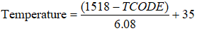
Unit is Celsius.
7.7 System Pinmux control
There are totally 64 pins can be set as Multiplex Peripheral Pins. Multiplex Peripheral Pins include ETH_SW, SDIO, PWM, Input Capture, SPI MASTER, SPI SLAVE, I2C MASTER, UART(1~4), TIMER, GPIO INT functions. This function can be controlled by Group2~3 registers. Please refer to chapter 5 for detail description of this function.
...
If user set Group1.1[5] as "1". the pin92~97 will become EMMC function interface.
7.
...
8 System GPIO control
There are totally 72 GPIO pins which are separated into 9 I/O ports, and each port contains 8 GPIO signals. The I/O driving capability for signals in GPIO0 is 16mA and 8mA for those in other GPIO ports. All 72 GPIO signals are Tri-state Output with Schmitt Trigger Input. The GPIO can be controlled by Group6~7 registers. Please refer to chapter 5 for detail description of this function.
7.9 Core Clock Divide Enable
...
There has a special mode to divide core clock to half. Core clock is generated by dividing pll clock, so set pll cleck to half, it will let core clock become half also. The control bit is CORECLK_DIV2_EN which map to 0x9EC0000C[10]. 0: Pll cleck, 1: Pll clock/2.
7.10 Registers Map
7.
...
10.1 Registers Memory Map
Address | Group No. | Register Name | Register Description |
0x9C000000 | G0.0 | mo stamp | Chip Revision Stamp ID Register |
0x9C000004 | G0.1 | mo clken0 | Clock Enable Register #0 |
0x9C000008 | G0.2 | mo clken1 | Clock Enable Register #1 |
0x9C00000C | G0.3 | mo clken2 | Clock Enable Register #2 |
0x9C000010 | G0.4 | mo clken3 | Clock Enable Register #3 |
0x9C000014 | G0.5 | mo clken4 | Clock Enable Register #4 |
0x9C000018 | G0.6 | mo clken5 | Clock Enable Register #5 |
0x9C00001C | G0.7 | mo clken6 | Clock Enable Register #6 |
0x9C000020 | G0.8 | mo clken7 | Clock Enable Register #7 |
0x9C000024 | G0.9 | mo clken8 | Clock Enable Register #8 |
0x9C000028 | G0.10 | mo clken9 | Clock Enable Register #9 |
0x9C00002C | G0.11 | mo gclken0 | Clock Gating Enable Register #0 |
0x9C000030 | G0.12 | mo gclken1 | Clock Gating Enable Register #1 |
0x9C000034 | G0.13 | mo gclken2 | Clock Gating Enable Register #2 |
0x9C000038 | G0.14 | mo gclken3 | Clock Gating Enable Register #3 |
0x9C00003C | G0.15 | mo gclken4 | Clock Gating Enable Register #4 |
0x9C000040 | G0.16 | mo gclken5 | Clock Gating Enable Register #5 |
0x9C000044 | G0.17 | mo gclken6 | Clock Gating Enable Register #6 |
0x9C000048 | G0.18 | mo gclken7 | Clock Gating Enable Register #7 |
0x9C00004C | G0.19 | mo gclken8 | Clock Gating Enable Register #8 |
0x9C000050 | G0.20 | mo gclken9 | Clock Gating Enable Register #9 |
0x9C000054 | G0.21 | mo reset0 | Hardware Reset Control Register #0 |
0x9C000058 | G0.22 | mo reset1 | Hardware Reset Control Register #1 |
0x9C00005C | G0.23 | mo reset2 | Hardware Reset Control Register #2 |
0x9C000060 | G0.24 | mo reset3 | Hardware Reset Control Register #3 |
0x9C000064 | G0.25 | mo reset4 | Hardware Reset Control Register #4 |
0x9C000068 | G0.26 | mo reset5 | Hardware Reset Control Register #5 |
0x9C00006C | G0.27 | mo reset6 | Hardware Reset Control Register #6 |
0x9C000070 | G0.28 | mo reset7 | Hardware Reset Control Register #7 |
0x9C000074 | G0.29 | mo reset8 | Hardware Reset Control Register #8 |
0x9C000078 | G0.30 | mo reset9 | Hardware Reset Control Register #9 |
0x9C00007C | G0.31 | mo sft cfg mode | Software Configure Hardware Mode |
...
Address | Group No. | Register Name | Register Description |
0x9C000380 | G7.0 | gpio in inv 0 | GPIO Input Invert Register #0 |
0x9C000384 | G7.1 | gpio in inv 1 | GPIO Input Invert Register #1 |
0x9C000388 | G7.2 | gpio in inv 2 | GPIO Input Invert Register #2 |
0x9C00038C | G7.3 | gpio in inv 3 | GPIO Input Invert Register #3 |
0x9C000390 | G7.4 | gpio in inv 4 | GPIO Input Invert Register #4 |
0x9C000394 | G7.5 | gpio in inv 5 | GPIO Input Invert Register #5 |
0x9C000398 | G7.6 | gpio in inv 6 | GPIO Input Invert Register #6 |
0x9C00039C | G7.7 | gpio in inv 7 | GPIO Input Invert Register #7 |
0x9C0003A0 | G7.8 | gpio out inv 0 | GPIO Output Invert Register #0 |
0x9C0003A4 | G7.9 | gpio out inv 1 | GPIO Output Invert Register #1 |
0x9C0003A8 | G7.10 | gpio out inv 2 | GPIO Output Invert Register #2 |
0x9C0003AC | G7.11 | gpio out inv 3 | GPIO Output Invert Register #3 |
0x9C0003B0 | G7.12 | gpio out inv 4 | GPIO Output Invert Register #4 |
0x9C0003B4 | G7.13 | gpio out inv 5 | GPIO Output Invert Register #5 |
0x9C0003B8 | G7.14 | gpio out inv 6 | GPIO Output Invert Register #6 |
0x9C0003BC | G7.15 | gpio out inv 7 | GPIO Output Invert Register #7 |
0x9C0003C0 | G7.16 | gpio od 0 | GPIO OD Register #0 |
0x9C0003C4 | G7.17 | gpio od 1 | GPIO OD Register #1 |
0x9C0003C8 | G7.18 | gpio od 2 | GPIO OD Register #2 |
0x9C0003CC | G7.19 | gpio od 3 | GPIO OD Register #3 |
0x9C0003D0 | G7.20 | gpio od 4 | GPIO OD Register #4 |
0x9C0003D4 | G7.21 | gpio od 5 | GPIO OD Register #5 |
0x9C0003D8 | G7.22 | gpio od 6 | GPIO OD Register #6 |
0x9C0003DC | G7.23 | gpio od 7 | GPIO OD Register #7 |
0x9C0003E0 | G7.24 | rsv | Reserved |
0x9C0003E4 | G7.25 | rsv | Reserved |
0x9C0003E8 | G7.26 | rsv | Reserved |
0x9C0003EC | G7.27 | rsv | Reserved |
0x9C0003F0 | G7.28 | rsv | Reserved |
0x9C0003F4 | G7.29 | rsv | Reserved |
0x9C0003F8 | G7.30 | rsv | Reserved |
0x9C0003FC | G7.31 | rsv | Reserved |
7.
...
10.2 Registers Description
RGST Table Group 0 MOON
0.0 Chip Revision Stamp ID Register (mo stamp)
Address: 0x9C000000
Reset: 0x0000 0B10
...
Field Name | Bit | Access | Description |
| Mask bit | 31:16 | RW | Write valid bit for each LSB 16 bits The 16 bits map to corresponding LSB 16bits. Write 1 to valid the corresponding bit writing. |
| MO THERMAL PD TSENS | 15 | RW | Power down Temperature sensor 0: power on |
| MO THERMAL M MODE EN | 14 | RW | Enable the manual mode to shift the output code TCODE[10:0] 0: from the REG_AVE_CODE[10:0] |
| MO THERMAL FS SRA | 13 | RW | SARADC conversion control 0: end conversion |
| MO THERMAL EN SAR | 12 | RW | SARADC enable 0: disable |
| MO THERMAL EN CAL | 11 | RW | Enable calibration function at specific temperature 0: disable |
| MO THERMAL DC SHIFT | 10:8 | RW | Shift the SARADC sample/hold DC voltage |
| MO THERMAL DAC EN | 7 | RW | Enable the DAC ramp counter test mode 0: disable |
| MO THERMAL DAC CAL EN | 6 | RW | DAC calibration mode enable 0: disable |
| Reserved | 5 | RW | Reserved |
| MO THERMAL CHOP EN | 0 | RW | TSEN chopper function 0: disable chopper function |
5.1 Thermal Control register #1 (mo5 thermal ctl 1)
Address: 0x9C000284
Reset: 0x0000 A14B
Field Name | Bit | Access | Description |
| Mask bit | 31:16 | RW | Write valid bit for each LSB 16 bits The 16 bits map to corresponding LSB 16bits. Write 1 to valid the corresponding bit writing. |
| Reserved | 15 | RW | RESERVED |
| MO THERMAL REG AVE CODE | 14:4 | RW | Enable the code average function 0: disable |
| MO THERMAL REG ADR | 3:0 | RW | The memory address |
...
Field Name | Bit | Access | Description |
| Mask bit | 31:16 | RW | Write valid bit for each LSB 16 bits The 16 bits map to corresponding LSB 16bits. Write 1 to valid the corresponding bit writing. |
| Reserved | 15 | RW | RESERVED |
| MO THERMAL TDEC | 14:12 | RW | Trimming VBE voltage |
| MO THERMAL RESERVE | 11:4 | RW | Reserve pin |
| MO THERMAL REG UD | 3 | RW | DAC test mode Up/down counter function |
| MO THERMAL REG AVE MODE | 2:1 | RW | Average function 0x0: 4 rimes |
| MO THERMAL REG AVE CODE EN | 0 | RW | Enable the code average function 0: disable |
5.3 Thermal Control register #3 (mo5 thermal ctl 3)
Address: 0x9C00028C
...
Field Name | Bit | Access | Description |
| Mask bit | 31:16 | RW | Write valid bit for each LSB 16 bits The 16 bits map to corresponding LSB 16bits. Write 1 to valid the corresponding bit writing. |
| Reserved | 15 | RW | RESERVED |
| MO THERMAL WR EN | 14 | RW | Enable the memory to write data 0: disable |
MO THERMAL WR DATA | 13:6 | RW | The memory input data |
MO THERMAL VBG SEL | 5:3 | RW | VBG voltage select |
MO THERMAL VBE SEL | 2:1 | RW | VBE voltage select 0x0: VBEX1 |
MO THERMAL TEST | 0 | RW | Enable SARADC test mode 0: SARADC input from TSEN |
5.4 TMDS L2SW Control Register (mo5 tmds l2sw ctl)
Address: 0x9C000290
Reset: 0x0000 0000
...
Field Name | Bit | Access | Description |
| Mask bit | 31:16 | RW | Write valid bit for each LSB 16 bits The 16 bits map to corresponding LSB 16bits. Write 1 to valid the corresponding bit writing. |
Reserved | 15:4 | RW | RESERVED |
MO CLKRMIITX1 INV | 3 | RW | Port1 RMII TXCLK invert 0: non invert |
MO CLKRMIITX0 INV | 2 | RW | Port0 RMII TXCLK invert 0: non invert |
MO CLKRMIIRX1 INV | 1 | RW | Port1 RMII RXCLK invert 0: non invert |
MO CLKRMIIRX0 INV | 0 | RW | Port0 RMII RXCLK invert 0: non invert |
5.6 I2C2BUS Control Register (mo5 I2C2BUS ctl)
Address: 0x9C000298
Reset: 0x0
Field Name | Bit | Access | Description |
| Mask bit | 31:16 | RW | Write valid bit for each LSB 16 bits The 16 bits map to corresponding LSB 16bits. Write 1 to valid the corresponding bit writing. |
Reserved | 15:8 | RW | RESERVED |
MO I2C2BUS INVERSE | 7 | RW | I2CBUS Byte inverse 0: normal(default) |
MO I2C2BUS FILER | 6:4 | RW | The filter of I2C input port SCL and SDA 0x0: 0 continuous same data input (default) |
MO DRAM B SIZE | 3:2 | RW | DRAM 1 Size Control 0x0: 128MB |
MO DRAM A SIZE | 1:0 | RW | DRAM 0 Size Control 0x0: 128MB |
5.7 PFCNT Register (pfcnt ctl)
Address: 0x9C00029C
...
Field Name | Bit | Access | Description |
| Mask bit | 31:16 | RW | Write valid bit for each LSB 16 bits The 16 bits map to corresponding LSB 16bits. Write 1 to valid the corresponding bit writing. |
| Reserved | 15 | RW | Reserved |
| MO PFCNT SENSOR INT CLR | 14 | RW | PFCNT SENSOR interrupt write 1 clear |
| MO RG PFCNT SENSE EN | 13 | RW | PFCNT SENSE enable 0: disable(default) |
| MO RG PFCNT FS | 12:10 | RW | PFCNT Macro Frequency Setting 0x0: 1T |
| MO RG PFCNT PD N | 9 | RW | PFCNT Macro Power Enable 0:Power down(default) |
| MO RG PFCNT RST N | 8 | RW | PFCNT Macro Reset Enable 0: Reset |
| MO RG PFCNT RSVI | 7:0 | RW | PFCNT Macro Reserved Input |
...
Field Name | Bit | Access | Description |
| Mask bit | 31:16 | RW | Write valid bit for each LSB 16 bits The 16 bits map to corresponding LSB 16bits. Write 1 to valid the corresponding bit writing. |
MO DC09 OPTION | 15 | RW | Spare register |
MO DC09 EN OCP | 14 | RW | Enable the current-limit detector function 0:Disable(Default) |
MO DC09 EN COMP | 13 | RW | Enable the comparator for temperature-limit, current-limit, power good and LVD 0:Disable(Default) |
MO DC09 EN TMP PROT | 12 | RW | Enable the temperature-limit protect function 0:Disable(Default) |
MO DC09 VREF OCP | 11:10 | RW | The current-limit trip point 0x0: 700mA |
Reserved | 9:7 | RW | RESERVED |
MO DC09 ENB DRVN | 6 | RW | Under-shoot protect 0:Enable |
Reserved | 5 | RW | RESERVED |
MO DC09 VREF SS | 4:3 | RW | Power ready reference voltage. 0x0: 0.844V(Default) |
MO DC09 EN OCP PROT | 2 | RW | Enable the comparator for temperature-limit, current-limit, power good and LVD 0:Disable(Default) |
Reserved | 1 | RW | RESERVED |
Reserved | 0 | RW | RESERVED |
...
Field Name | Bit | Access | Description |
| Mask bit | 31:16 | RW | Write valid bit for each LSB 16 bits The 16 bits map to corresponding LSB 16bits. Write 1 to valid the corresponding bit writing. |
| MO DC09 PWFM | 15 | RW | PWM or PFM select 0: PWM (default) |
| MO DC09 EN TMP | 14 | RW | Enable the temperature-limit detector function 0:Disable(Default) |
| MO DC09 PWMHYSEN | 13:11 | RW | Triangle wave generator comparator hysteresis window setting. 0x0:80mV(Default) |
| MO DC09 OCP HYS | 10:9 | RW | The hysteresis for current-limit trip point 0x0: 1.6%(Default) |
| MO DC09 N | 8:6 | RW | OSC frequency adjust, actual frequency variation is less then 20%. 0x0:429KHz (Default) |
| MO DC09 TMP HYS | 5:4 | RW | The hysteresis for thermal-limit trip point 0x0:5C (Default) |
| MO DC09 T TMP | 3:2 | RW | The thermal-shutdown trip point 0x0:125C(Default.) |
| MO DC09 VREF LVD | 1:0 | RW | Low voltage reference voltage. 0x0:0.706V |
5.25 DC 0.9V Control Register #2 (DC09 CTL 2)
Address: 0x9C0002E4
Reset: 0x0
Field Name | Bit | Access | Description |
| Mask bit | 31:16 | RW | Write valid bit for each LSB 16 bits The 16 bits map to corresponding LSB 16bits. Write 1 to valid the corresponding bit writing. |
| Reserved | 15:10 | RW | RESERVED |
DC09 LVD OUT | 9 | RO | Indicate the output voltage are low voltage or not. (control by VREF LVD[1:0]) 0:no low voltage |
DC09 READY | 8 | RO | Indicate the output voltage are power good or not. (control by VREF SS[1:0]) 0:not power good |
DC09 TMP OUT | 7 | RO | Indicate the output voltage are over-temperature or not. (control by T TMP[1:0]) 0:no over-temperature |
DC09 OCP OUT | 6 | RO | Indicate the output voltage are over-current or not. (control by VREF OCP[1:0]) 0:no over-current |
MO DC09 TRLVLADJ | 5:3 | RW | Reference voltage of Duty in PFM. 0x0:1.3458V(Default.) |
MO DC09 SFTHYSEN | 2:0 | RW | Soft-start comparator hysteresis window setting. |
5.26 DC 1.2V Control Register #0 (DC12 CTL 0)
Address: 0x9C0002E8
Reset: 0x0
Field Name | Bit | Access | Description |
| Mask bit | 31:16 | RW | Write valid bit for each LSB 16 bits The 16 bits map to corresponding LSB 16bits. Write 1 to valid the corresponding bit writing. |
| MO DC12 OPTION | 15 | RW | Spare register |
| MO DC12 EN OCP | 14 | RW | Enable the current-limit detector function 0:Disable(Default) |
| MO DC12 EN COMP | 13 | RW | Enable the comparator for temperature-limit, current-limit, power good and LVD 0:Disable(Default) |
| MO DC12 EN TMP PROT | 12 | RW | Enable the temperature-limit protect function 0:Disable(Default) |
| MO DC12 VREF OCP | 11:10 | RW | The current-limit trip point 0x0: 700mA |
Reserved | 9:7 | RW | RESERVED |
MO DC12 ENB DRVN | 6 | RW | Under-shoot protect 0:Enable |
MO DC12 ENB DRVP | 5 | RW | Over-shoot protect: 0:Enable |
MO DC12 VREF SS | 4:3 | RW | Power ready reference voltage. 0x0: 0.844V(Default.) |
MO DC12 EN OCP PROT | 2 | RW | Enable the comparator for temperature-limit, current-limit, power good and LVD 0:Disable(Default.) |
Reserved | 1 | RW | RESERVED |
Reserved | 0 | RW | RESERVED |
...
Field Name | Bit | Access | Description |
| Mask bit | 31:16 | RW | Write valid bit for each LSB 16 bits The 16 bits map to corresponding LSB 16bits. Write 1 to valid the corresponding bit writing. |
| MO DC12 PWFM | 15 | RW | PWM or PFM select 0: PWM (default) |
| MO DC12 EN TMP | 14 | RW | Enable the temperature-limit detector function 0:Disable(Default.) |
| MO DC12 PWMHYSEN | 13:11 | RW | Triangle wave generator comparator hysteresis window setting. 0x0:80mV(Default) |
MO DC12 OCP HYS | 10:9 | RW | The hysteresis for current-limit trip point 0x0: 1.6%(Default.) |
MO DC12 N | 8:6 | RW | OSC frequency adjust, actual frequency variation is less then 20%. 0x0:429KHz (Default) |
MO DC12 TMP HYS | 5:4 | RW | The hysteresis for thermal-limit trip point 0x0:5C (Default) |
MO DC12 T TMP | 3:2 | RW | The thermal-shutdown trip point 0x0:125C(Default.) |
MO DC12 VREF LVD | 1:0 | RW | Low voltage reference voltage. 0x0:0.706V |
5.28 DC 1.2V Control Register #2 (DC12 CTL 2)
Address: 0x9C0002F0
Reset: 0x0
Field Name | Bit | Access | Description |
| Mask bit | 31:16 | RW | Write valid bit for each LSB 16 bits The 16 bits map to corresponding LSB 16bits. Write 1 to valid the corresponding bit writing. |
| Reserved | 15:10 | RW | RESERVED |
| DC12 LVD OUT | 9 | RW | Indicate the output voltage are low voltage or not (control by VREF LVD[1:0]). 0:no low voltage |
| DC12 READY | 8 | RW | Indicate the output voltage are power good or not. (control by VREF SS[1:0]) 0:not power good |
| DC12 TMP OUT | 7 | RW | Indicate the output voltage are over-temperature or not. (control by T TMP[1:0]) 0:no over-temperature |
| DC12 OCP OUT | 6 | RW | Indicate the output voltage are over-current or not. (control by VREF OCP[1:0]) 0:no over-current |
MO DC12 TRLVLADJ | 5:3 | RW | Reference voltage of Duty in PFM. 0x0:1.3458V(Default.) |
MO DC12 SFTHYSEN | 2:0 | RW | Soft-start comparator hysteresis window setting. 0x0:80mV(Default) |
5.29 DC 1.5V Control Register #0 (DC15 CTL 0)
Address: 0x9C0002F4
Reset: 0x0
Field Name | Bit | Access | Description |
| Mask bit | 31:16 | RW | Write valid bit for each LSB 16 bits The 16 bits map to corresponding LSB 16bits. Write 1 to valid the corresponding bit writing. |
| MO DC15 OPTION | 15 | RW | Spare register |
| Reserved | 14:10 | RW | RESERVED |
| Reserved | 9:7 | RW | RESERVED |
MO DC15 ENB DRVN | 6 | RW | Under-shoot protect 0:Enable |
MO DC15 ENB DRVP | 5 | RW | Over-shoot protect: 0:Enable |
MO DC15 VREF SS | 4:3 | RW | Power ready reference voltage. 0x0: 0.844V(Default.) |
Reserved | 2 | RW | RESERVED |
Reserved | 1 | RW | RESERVED |
Reserved | 0 | RW | RESERVED |
...
Field Name | Bit | Access | Description |
| Mask bit | 31:16 | RWRW | Write valid bit for each LSB 16 bits The 16 bits map to corresponding LSB 16bits. Write 1 to valid the corresponding bit writing. |
| MO DC15 PWFM | 15 | RW | PWM or PFM select 0: PWM (default) |
| Reserved | 14 | RW | RESERVED |
| MO DC15 PWMHYSEN | 13:11 | RW | Triangle wave generator comparator hysteresis window setting. 0x0:80mV(Default) |
| Reserved | 10:9 | RW | RESERVED |
| MO DC15 N | 8:6 | RW | OSC frequency adjust, actual frequency variation is less then20%. 0x0:429KHz (Default) |
| Reserved | 5:4 | RW | RESERVED |
| MO DC15 T TMP | 3:2 | RW | The thermal-shutdown trip point 0x0:125C(Default.) |
| MO DC15 VREF LVD | 1:0 | RW | Low voltage reference voltage. 0x0:0.706V |
5.31 DC 1.5V Control Register #2 (DC15 CTL 2)
Address: 0x9C0002FC
...
Field Name | Bit | Access | Description |
| Mask bit | 31:16 | RW | Write valid bit for each LSB 16 bits The 16 bits map to corresponding LSB 16bits. Write 1 to valid the corresponding bit writing. |
| Reserved | 15:8 | RW | RESERVED |
DC15 LVD OUT | 7 | RW | Indicate the output voltage are low voltage or not (control by VREF LVD[1:0]). 0:no low voltage |
DC15 READY | 6 | RW | Indicate the output voltage are power good or not. (control by VREF SS[1:0]) 0:not power good |
MO DC15 TRLVLADJ | 5:3 | RW | Reference voltage of Duty in PFM. 0x0:1.3458V(Default.) |
MO DC15 SFTHYSEN | 2:0 | RW | Soft-start comparator hysteresis window setting. 0x0:80mV(Default) |
RGST Table Group 6 GPIOXT
6.0 GPIO Control Source Selection Register #0 (gpio ctl sel 0)
Address: 0x9C000300
Reset: 0xFFFF FFFF
...