...
SP7021 embedded 3 DC2DC modules, they are 3.3V to 0.9V, 3.3V to 1.2V and 3.3V to 1.5V. So SP7021 just need one single power supply that is 3.3V. The parameters can be set by Group5.23~31 registers.
7.6 Thermal sensor control
SP7021 embedded a thermal sensor which operation temperature range between -40°C ~125°C. The resolution is 1°C. The parameters can be set by Group5 registers.
For example, when MO_THERMAL_VBE_SEL=0x01(default), then read TCODE value from G5.12[10:0] and calculate chip temperature as below:
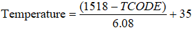
Unit is Celsius.
7.7 System Pinmux control
There are totally 64 pins can be set as Multiplex Peripheral Pins. Multiplex Peripheral Pins include ETH_SW, SDIO, PWM, Input Capture, SPI MASTER, SPI SLAVE, I2C MASTER, UART(1~4), TIMER, GPIO INT functions. This function can be controlled by Group2~3 registers. Please refer to chapter 5 for detail description of this function.
...
If user set Group1.1[5] as "1". the pin92~97 will become EMMC function interface.
7.
...
8 System GPIO control
There are totally 72 GPIO pins which are separated into 9 I/O ports, and each port contains 8 GPIO signals. The I/O driving capability for signals in GPIO0 is 16mA and 8mA for those in other GPIO ports. All 72 GPIO signals are Tri-state Output with Schmitt Trigger Input. The GPIO can be controlled by Group6~7 registers. Please refer to chapter 5 for detail description of this function.
7.
...
9 Registers Map
7.
...
9.1 Registers Memory Map
Address | Group No. | Register Name | Register Description |
0x9C000000 | G0.0 | mo stamp | Chip Revision Stamp ID Register |
0x9C000004 | G0.1 | mo clken0 | Clock Enable Register #0 |
0x9C000008 | G0.2 | mo clken1 | Clock Enable Register #1 |
0x9C00000C | G0.3 | mo clken2 | Clock Enable Register #2 |
0x9C000010 | G0.4 | mo clken3 | Clock Enable Register #3 |
0x9C000014 | G0.5 | mo clken4 | Clock Enable Register #4 |
0x9C000018 | G0.6 | mo clken5 | Clock Enable Register #5 |
0x9C00001C | G0.7 | mo clken6 | Clock Enable Register #6 |
0x9C000020 | G0.8 | mo clken7 | Clock Enable Register #7 |
0x9C000024 | G0.9 | mo clken8 | Clock Enable Register #8 |
0x9C000028 | G0.10 | mo clken9 | Clock Enable Register #9 |
0x9C00002C | G0.11 | mo gclken0 | Clock Gating Enable Register #0 |
0x9C000030 | G0.12 | mo gclken1 | Clock Gating Enable Register #1 |
0x9C000034 | G0.13 | mo gclken2 | Clock Gating Enable Register #2 |
0x9C000038 | G0.14 | mo gclken3 | Clock Gating Enable Register #3 |
0x9C00003C | G0.15 | mo gclken4 | Clock Gating Enable Register #4 |
0x9C000040 | G0.16 | mo gclken5 | Clock Gating Enable Register #5 |
0x9C000044 | G0.17 | mo gclken6 | Clock Gating Enable Register #6 |
0x9C000048 | G0.18 | mo gclken7 | Clock Gating Enable Register #7 |
0x9C00004C | G0.19 | mo gclken8 | Clock Gating Enable Register #8 |
0x9C000050 | G0.20 | mo gclken9 | Clock Gating Enable Register #9 |
0x9C000054 | G0.21 | mo reset0 | Hardware Reset Control Register #0 |
0x9C000058 | G0.22 | mo reset1 | Hardware Reset Control Register #1 |
0x9C00005C | G0.23 | mo reset2 | Hardware Reset Control Register #2 |
0x9C000060 | G0.24 | mo reset3 | Hardware Reset Control Register #3 |
0x9C000064 | G0.25 | mo reset4 | Hardware Reset Control Register #4 |
0x9C000068 | G0.26 | mo reset5 | Hardware Reset Control Register #5 |
0x9C00006C | G0.27 | mo reset6 | Hardware Reset Control Register #6 |
0x9C000070 | G0.28 | mo reset7 | Hardware Reset Control Register #7 |
0x9C000074 | G0.29 | mo reset8 | Hardware Reset Control Register #8 |
0x9C000078 | G0.30 | mo reset9 | Hardware Reset Control Register #9 |
0x9C00007C | G0.31 | mo sft cfg mode | Software Configure Hardware Mode |
...
Address | Group No. | Register Name | Register Description |
0x9C000380 | G7.0 | gpio in inv 0 | GPIO Input Invert Register #0 |
0x9C000384 | G7.1 | gpio in inv 1 | GPIO Input Invert Register #1 |
0x9C000388 | G7.2 | gpio in inv 2 | GPIO Input Invert Register #2 |
0x9C00038C | G7.3 | gpio in inv 3 | GPIO Input Invert Register #3 |
0x9C000390 | G7.4 | gpio in inv 4 | GPIO Input Invert Register #4 |
0x9C000394 | G7.5 | gpio in inv 5 | GPIO Input Invert Register #5 |
0x9C000398 | G7.6 | gpio in inv 6 | GPIO Input Invert Register #6 |
0x9C00039C | G7.7 | gpio in inv 7 | GPIO Input Invert Register #7 |
0x9C0003A0 | G7.8 | gpio out inv 0 | GPIO Output Invert Register #0 |
0x9C0003A4 | G7.9 | gpio out inv 1 | GPIO Output Invert Register #1 |
0x9C0003A8 | G7.10 | gpio out inv 2 | GPIO Output Invert Register #2 |
0x9C0003AC | G7.11 | gpio out inv 3 | GPIO Output Invert Register #3 |
0x9C0003B0 | G7.12 | gpio out inv 4 | GPIO Output Invert Register #4 |
0x9C0003B4 | G7.13 | gpio out inv 5 | GPIO Output Invert Register #5 |
0x9C0003B8 | G7.14 | gpio out inv 6 | GPIO Output Invert Register #6 |
0x9C0003BC | G7.15 | gpio out inv 7 | GPIO Output Invert Register #7 |
0x9C0003C0 | G7.16 | gpio od 0 | GPIO OD Register #0 |
0x9C0003C4 | G7.17 | gpio od 1 | GPIO OD Register #1 |
0x9C0003C8 | G7.18 | gpio od 2 | GPIO OD Register #2 |
0x9C0003CC | G7.19 | gpio od 3 | GPIO OD Register #3 |
0x9C0003D0 | G7.20 | gpio od 4 | GPIO OD Register #4 |
0x9C0003D4 | G7.21 | gpio od 5 | GPIO OD Register #5 |
0x9C0003D8 | G7.22 | gpio od 6 | GPIO OD Register #6 |
0x9C0003DC | G7.23 | gpio od 7 | GPIO OD Register #7 |
0x9C0003E0 | G7.24 | rsv | Reserved |
0x9C0003E4 | G7.25 | rsv | Reserved |
0x9C0003E8 | G7.26 | rsv | Reserved |
0x9C0003EC | G7.27 | rsv | Reserved |
0x9C0003F0 | G7.28 | rsv | Reserved |
0x9C0003F4 | G7.29 | rsv | Reserved |
0x9C0003F8 | G7.30 | rsv | Reserved |
0x9C0003FC | G7.31 | rsv | Reserved |
7.
...
9.2 Registers Description
RGST Table Group 0 MOON
0.0 Chip Revision Stamp ID Register (mo stamp)
Address: 0x9C000000
Reset: 0x0000 0B10
...