15.1 Introduction
The SP7021 utilizes system in package (SIP) technology to provide an internal buffer SDARM within the package. The SP7021 supports 1Gb and 4Gb of internal SDRAMs. The SDRAM is DDR3 (Double Data Rate 3) 1066max type and uses a 16-bit data interface. 16-bit and 8-bit data interfaces are both supported. It supports DFI2.1 to DRAM controller with DFI and PHY clock ratio is 1:2 and 1:1. The DRAM memory map area locates at address 0x00000000~0x1FFFFFFF which have 512MB size. The control registers address locates at 0x9C001900~0x9C001AFF.
15.2 Function Diagram
The SP7021 DRAM controller used uMCTL2 IP and the function diagram is shown in Figure 15-1. The uMCTL2 receives transactions from the SoC core. These transactions are queued internally and scheduled for access in order to the SDRAM while satisfying the SDRAM protocol timing requirements, transaction priorities, and dependencies between the transactions. The uMCTL2 issues commands on the DFI interface to the PHY module, which launches and captures data to and from the SDRAM.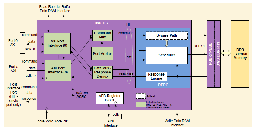
Figure 15-1 DRAM Controller Functional Blocks
The uMCTL2 contains the following main architectural components
- The AXI Port Interface (XPI) block: This block provides the interface to the application ports. It provides bus protocol handling, data buffering and reordering for read data, data bus size conversion (upsizing or downsizing), and memory burst address alignment. Read data is stored in a SRAM, read re-order buffer and returned in order, to the AXI ports. The SRAM may be instantiated as embedded memory external to the uMCTL2 or implemented as flops within the uMCTL2.
- The Port Arbiter (PA) block: This block provides latency sensitive, priority based arbitration between the addresses issued by the XPIs (by the ports).
- The DDR Controller (DDRC) block: This block contains a logical CAM (Content Addressable Memory), which can be synthesized using standard cells. This holds information on the commands, which is used by the scheduling algorithms to optimally schedule commands to be sent to the PHY, based on priority, bank/rank status and DDR timing constraints. A bypass path is also provided (optionally).
- The APB Register Block: This block contains the software accessible registers.
The DDR PHY is designed to connect the DRAM (dynamic random access memory) controller and DDR (Double Data Rate) 3 DRAM device. It contains the DDR PHY Control Unit (DPCU) and the Analog part (APHY). The interface between DRAM controller and the DDR PHY is compliant with DFI 2.1(DDR PHY Interface) protocol. The DDR PHY includes APHY initialization, data training, DRAM initialization, hardware VT compensation, and hardware auto timing update functionalities, as is used to enhance the whole DRAM system and to become robust and reliable. Figure 15-2 shows a DDR PHY block diagram.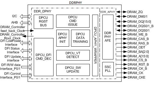
Figure 15-2 DDR PHY Block Diagram
- DPCU_DFI_CMD_DEC: This module is used to decode DFI commands from DRAM controller for DRAM device.
- DPCU_APHY_INIT: DPCU_APHY_INIT controls the initial flow for analog part (APHY).
- DPCU_DATA_TRAINING: This is the crucial part of DDRPHY, and it is used to do data training, which is the process to acquire optimal timing between signals for DRAM write/read transactions.
- DPCU_CMD_ISSUE: This module works like a lite DRAM controller. It can generate DRAM commands and the timing between those commands is guaranteed to meet DRAM specification.
- DPCU_VT_DETECT: Since process, voltage and temperature can deviate the delay of delay cells, this module is used to compensate those non-ideal effects.
- DPCU_SW_UPDATE: If the system need to change some settings of delay cells by software, this module can update those settings in a suitable period.
- DPCU_RGST_BUS: The communication interface between CPU and DDRPHY.
- DPCU_APHY_WRAPPER: The interface between DPCU and APHY.
- DDR_APHY: Analog part of DDRPHY which provide the interface with DDR device.
15.3 DRAM Bus Signals Dynamic Swap in DDRPHY pins
Although SP7021 will SIP DDR3 inside the chip, for compatible more commercial DDR3 KGD, SP7021 can adjust pad location for more easier bonding through registers setting. The control registers are Group50.27~31.
For example, Group50.29 register bit[31:27] can select which DRAM signals ouput to DRAM_A3 pin.
| A3 SWAP | 31:27 | RW | control DRAM A3 swap |
select one DRAM BUS signal to through DRAM A3 pin; | |||
default value is 0xc, represent DRAM A3 signal through | |||
DRAM A3 pin; | |||
0x0: select DRAM CKE signal through DRAM A3 pin; | |||
0x1: select DRAM ODT signal through DRAM A3 pin; | |||
0x2: select DRAM CS N signal through DRAM A3 pin; | |||
0x3: select DRAM RAS N signal through DRAM A3 pin; | |||
0x4: select DRAM CAS N signal through DRAM A3 pin; | |||
0x5: select DRAM WE N signal through DRAM A3 pin; | |||
0x6: select DRAM BA0 signal through DRAM A3 pin; | |||
0x7: select DRAM BA1 signal through DRAM A3 pin; | |||
0x8: select DRAM BA2 signal through DRAM A3 pin; | |||
0x9: select DRAM A0 signal through DRAM A3 pin; | |||
0xa: select DRAM A1 signal through DRAM A3 pin; | |||
0xb: select DRAM A2 signal through DRAM A3 pin; | |||
0xc: select DRAM A3 signal through DRAM A3 pin; | |||
0xd: select DRAM A4 signal through DRAM A3 pin; | |||
0xe: select DRAM A5 signal through DRAM A3 pin; | |||
0xf: select DRAM A6 signal through DRAM A3 pin; | |||
0x10: select DRAM A7 signal through DRAM A3 pin; | |||
0x11: select DRAM A8 signal through DRAM A3 pin; | |||
0x12: select DRAM A9 signal through DRAM A3 pin; | |||
0x13: select DRAM A10 signal through DRAM A3 pin; | |||
0x14: select DRAM A11 signal through DRAM A3 pin; | |||
0x15: select DRAM A12 signal through DRAM A3 pin; | |||
0x16: select DRAM A13 signal through DRAM A3 pin; | |||
0x17: select DRAM A14 signal through DRAM A3 pin; | |||
0x18: select DRAM A15 signal through DRAM A3 pin; |
15.4 Registers Map
RGST Table Group 50DDR PHY-A Control Unit G1
50.0 DPCU Global Setting (dpcu glo set)
Address: 0x9C001900
Reset: 0x5432 AA21
| Field Name | Bit | Access | Description |
| DPCU RI QS LATE WIN SEL | 31:30 | RW | RDQSG late window selection |
| DPCU RI QS EARLY WIN SEL | 29:28 | RW | RDQSG early window selection |
| RESERVED | 27 | RO | reserved |
| DPCU RI SIP MODE | 26 | RW | SIP/non-SIP mode selection |
| RESERVED | 25:22 | RO | reserved |
| DX SERDES EN | 21:20 | RW | Date serdes enable [20]: 1'b1 = DX0 enable [21]: 1'b1 = DX1 enable [22]: 1'b1 = DX2 enable (reserved) [23]: 1'b1 = DX3 enable (reserved) |
| DPCU RI QS GATE EXTEN | 19 | RW | RDQS gate extention |
RF MODE EN | 18 | RW | DFI Interface signal transfer mode |
RGST AI PZQ IO DIS | 17 | RW | disable IO during PZQ calibration |
|
|
|
|
|
|
|
|
|
|
|
|
|
|
|
|
DIS VT CALIB | 4 | RW | Disable VT dynamic calibration function |
RESERVED | 3 | RO | reserved |
|
|
|
|
RESERVED | 1 | RW | reserved |
|
|
|
|
50.1 DPCU Initial control (dpcu init ctrl)
Address: 0x9C001904
Reset: 0x0000 0012
| Field Name | Bit | Access | Description |
| RESERVED | 31:16 | RO | reserved |
| RGST AI PZQ INIT BYPASS | 15 | RW | Bypass DPCU do PZQ initial sequence |
| RGST AI DDL INIT BYPASS | 14 | RW | Bypass DPCU do DDL initial sequence |
| RGST AI SSCPLL INIT BYPASS | 13 | RW | Bypass DPCU do SSCPLL initial sequence |
| RGST AI CTCAL INIT | 12 | RW | Bypass DPCU do CTCAL initial sequence |
| RGST AI PZQ INIT EN | 11 | RW | Enable DPCU do PZQ initial sequence. Self clean |
| RGST AI DDL INIT EN | 10 | RW | Enable DPCU do DDL initial sequence. Self clean |
| RGST AI SSCPLL INIT EN | 9 | RW | Enable DPCU do SSCPLL initial sequence. Self clean |
| RGST AI CTCAL INIT EN | 8 | RW | Enable DPCU do CTCAL initial sequence. Self clean |
| RESERVED | 7:6 | RO | |
| RGST AI RST SW FORCE | 5 | RW | force AI RST as 1 |
| RGST AI RST SYNC EN | 4 | RW | Enable DPCU AI switch MEM RST SYNC source 0 : always from Global reset 1 : enable (default) |
| RESERVED | 3 | RO | |
| RGST AI APHY INIT START | 2 | RW | DPCU AI start to do initial sequence. Self clear when DPCU AI finish. |
| RGST AI APHY INIT RST B | 1 | RW | DPCU AI SW reset. If this signal assert, all of the DPCU APHY INIT status will enter reset state. (active low) |
| RGST AW APHY SW CTRL | 0 | RW | APHY INIT flow from SW or DPCU 0 : initial signals are controlled by DPCU (default) 1 : initial signals are controlled by SW |
50.2 DPCU Initial status (dpcu init status)
Address: 0x9C001908
Reset: 0x0
| Field Name | Bit | Access | Description |
| RESERVED | 31:20 | RO | reserve |
APHY INIT ERROR INFO | 19:16 | RO | APHY initial error information |
APHY INIT STATE | 15:12 | RO | Debug information. Current DPCU AI main FSM value |
|
|
|
|
|
|
|
|
|
|
|
|
|
|
|
|
|
|
|
|
|
|
|
|
|
|
|
|
|
|
|
|
|
|
|
|
|
|
|
|
|
|
|
|
50.3 DPCU APHY Counter (dpcu aphy cnter)
Address: 0x9C00190C
Reset: 0x0005 0910
Field Name | Bit | Access | Description |
| RESERVED | 31:25 | RO | reserved |
DPCU RST TIMMER | 24:20 | RW | no specific function at V2.0. |
| DPCU INI TIMMER | 19:0 | RW | APHY Initial Timmer. Inclusive of PZQ, SSCPLL and DLL. |
50.4 DPCU DDL Calibration Global Setting (dpcu ddl calib set)
Address: 0x9C001910
Reset: 0x00F0 F0F3
| Field Name | Bit | Access | Description |
| RESERVED | 31:28 | RO | reserved |
| DPCU DDL CAL OFF TIME | 27:20 | RW | Number of clock cycles that the calibration data is closed |
| DPCU DDL CAL ON TIME | 19:12 | RW | Number of clock cycles that the calibration data is opened |
| DPCU DDL GCK EN TIME | 11:4 | RW | Number of clock cycles that the calibration clock is turned on |
| RESERVED | 3:2 | RO | reserved |
| DPCU DDL AVG NUM | 1:0 | RW | repeat number of DDL calibartion. |
50.5 DPCU SSCPLL setting - 1 (dpcu sscpll ctrl1)
Address: 0x9C001914
Reset: 0x0
Field Name | Bit | Access | Description |
| RESERVED | 31:28 | RO | reserved |
DPCU RI SSCPLL GAIN | 27:19 | RW | |
| DPCU RI SSCPLL SDM RST SEL | 18:17 | RW | |
| DPCU RI SSCPLL LOW BOUND | 16:0 | RW |
50.6 DPCU SSCPLL setting - 2 (dpcu sscpll ctrl2)
Address: 0x9C001918
Reset: 0x0
| Field Name | Bit | Access | Description |
| RESERVED | 31:20 | RO | reserved |
| DPCU RI SSCPLL EN MIXPHASE | 19 | RW | |
| DPCU RI SSCPLL SDM MODE | 18:17 | RW | |
| DPCU RI SSCPLL UP BOUND | 16:0 | RW |
50.7 DPCU Global reserved (reserved)
Address: 0x9C00191C
Reset: 0x0
| Field Name | Bit | Access | Description |
| RESERVED | 31:0 | RO | reserved |
50.8 APHY - Global (dpcu aphy glo)
Address: 0x9C001920
Reset: 0x00F0 0850
| Field Name | Bit | Access | Description |
| RESERVED | 31:24 | RO | |
| DPCU RI DX PDN | 23:20 | RW | Power down BPSD delay cell of DataSerDes 0 : power down 1 : enable (default) |
| DPCU RI DX PD | 19:16 | RW | Power down PSD and BDD delay cell of DataSerDes. 0 : enable (default) 1 : power down |
| RESERVED | 15:13 | RO | |
| DPCU RI AC SCAN SEL | 12 | RW | AC scan in data selection |
| DPCU RI QS DET RST N | 11 | RW | Reset RDQSG PSD early and late detection 0 : reset 1 : operation (default) |
| DPCU RI QS GLITCH MASK AON | 10 | RW | Always enable RDQSG glitch free mask 0 : control by DPCU (default) 1 : always on |
| RESERVED | 9:7 | RO | |
| DPCU RI AC PDN | 6 | RW | Power down BPSD delay cell of ACSerDes 0 : power down 1 : enable (default) |
| DPCU RI AC PD | 5 | RW | Power down PSD and BDD delay cell of ACSerDes. 0 : enable (default) 1 : power down |
| DPCU RI ACK PDN | 4 | RW | Power down BPSD delay cell of AC CK SerDes 0 : power down 1 : enable (default) |
| DPCU RI ACK PD | 3 | RW | Power down PSD and BDD delay cell of AC CK SerDes. 0 : enable (default) 1 : power down |
| DPCU RI APHY ACK RST B | 2 | RW | ACKSerDes SW reset(active low) |
| DPCU RI APHY AC RST B | 1 | RW | ACSerDes SW reset(active low) |
| DPCU RI APHY DX RST B | 0 | RW | All DataSerDes SW reset (active low) |
50.9 APHY MACRO Status Output 0 (dpcu aphy macro0)
Address: 0x9C001924
Reset: 0x0
Field Name | Bit | Access | Description |
| RESERVED | 31:30 | RO | reserved |
APHY RO CTCAL DDR R | 29:20 | RO | code value of ddr programmable delay line |
| APHY RO CTCAL DLL | 19:14 | RO | Delay line code output of DLL |
| APHY RO CTCAL JUST LWIN | 13 | RO | |
| APHY RO CTCAL JUST | 12 | RO | |
| APHY RO CTCAL LOTEST DPHY | 11 | RO | dphy clock low testing result |
| APHY RO CTCAL HITEST DPHY | 10 | RO | dphy clock high testing result |
| APHY RO CTCAL LATE | 9 | RO | Old CTCAL late |
| APHY RO CTCAL EARLY | 8 | RO | Old CTCAL early |
| APHY RO CTCAL COUNTER | 7:4 | RO | reserved |
| APHY RO CTCAL DLL LOCK | 3 | RO | Old CTCAL ddl lock |
| APHY RO CTCAL CALIB FAIL | 2 | RO | Old CTCAL calibration fail |
| APHY RO CTCAL CALIB DONE | 1 | RO | Old CTCAL calibration done |
| APHY MPLL LOCK OUT | 0 | RO | MPLL lock out signal |
50.10 APHY MACRO Status Output 1 (dpcu aphy macro1)
Address: 0x9C001928
Reset: 0x0
| Field Name | Bit | Access | Description |
| RESERVED | 31:24 | RO | reserved |
APHY RO PZQ ZCTRL | 23:8 | RO | Status of calibration result (coarse adjust): APHY RO PZQ ZCTRL[3:0] select the pull-down output impedance APHY RO PZQ ZCTRL[7:4] select the pull-up output impedance APHY RO PZQ ZCTRL[11:8] select the pull-down ODT impedance APHY RO PZQ ZCTRL[15:12] select the pull-up ODT Impedance |
APHY RO PZQ ZLSB | 7:4 | RO | Status of calibration result (fine adjust): |
|
|
|
|
|
|
|
|
|
|
|
|
50.11 APHY - MPLL 0 (dpcu aphy mpll0)
Address: 0x9C00192C
Reset: 0x0084 01C2
| Field Name | Bit | Access | Description |
| RESERVED | 31:24 | RO | |
| DPCU RI SSCPLL XTAL SELECT | 23 | RW | |
| DPCU RI SSCPLL REF TEST | 22 | RW | |
| DPCU RI MPLL BYPASS DCC | 21 | RW | |
| DPCU RI MPLL EN VDDCDCCAP | 20 | RW | |
| RESERVED | 19 | RO | |
| DPCU RI MPLL LDO DCC | 18 | RW | Enable the LDO 1V circuit for DCC 1.0V power |
| DPCU RI MPLL LDO TEST | 17 | RW | Test the LDO output voltage |
| DPCU RI MPLL VBG TEST | 16 | RW | Select Bandgap reference voltage test mode 0 : Normal mode (default) 1 : TEST mode |
| DPCU RI MPLL CNT SELECT | 15 | RW | Select the PLL loop lock cycle number 0 : 4096 (default) 1 : 2048 |
| DPCU RI MPLL G2 MODE | 14 | RW | Enable output pin x2x1 90, x2x1 180 and x2x1 270 |
| DPCU RI MPLL DTO MUX SEL | 13:12 | RW | Select output test signal 0x0 : sofg gnd, sofg gnd (default) 0x1 : phyclk, clkout test ck 0x2 : byp clkin, byp clkin 0x3 : test lock fb, test lock ref |
| DPCU RI MPLL TEST MODE | 11 | RW | Enable the test mode |
| DPCU RI MPLL BYP MODE | 10 | RW | MPLL bypass mode control 0 : Normal mode (default) 1 : Bypass mode |
| DPCU RI MPLL FC MODE | 9 | RW | HDR CLK full cycle mode 0 : inverse (default) 1 : inphase |
| DPCU RI MPLL PDN LOCK | 8 | RW | MPLL lock logic control 0 : power down 1 : operation (default) |
| DPCU RI MPLL PDN | 7 | RW | Power down signal 0 : disable PLL (power down) 1 : enable PLL (default) |
| DPCU RI MPLL PDN BGR | 6 | RW | Power down Bandgap reference. 0 : power down 1 : normal operation (default) |
| DPCU RI MPLL CAL MODE | 5 | RW | DX Calibration mode |
| DPCU RI MPLL RESET SEL | 4 | RW | MPLL reset path selection 0 : reset source is intercal lock detector (default) 1 : reset from DPCU |
| DPCU RI MPLL SSC TEST | 3 | RW | Rom code Test mode setting 0 : normal operation mode (default) 1 : external rom code test mode |
| DPCU RI MPLL SSCEN | 2 | RW | ssc enable control |
| DPCU RI MPLL DIV RST N | 1 | RW | MPLL divider soft reset (Low active) |
| DPCU RI MPLL RST N | 0 | RW | reset signal for SSCPLL loop |
50.12 APHY - MPLL 1 (dpcu aphy mpll1)
Address: 0x9C001930
Reset: 0x004E 5627
| Field Name | Bit | Access | Description |
| RESERVED | 31 | RO | |
| DPCU RI MPLL SP | 30:29 | RW | ssc spread rate setting |
| DPCU RI MPLL RES SEL | 28:26 | RW | Select Bandgap reference interior Res. |
| DPCU RI MPLL EMA | 25:23 | RW | Rom code option setting |
| DPCU RI MPLL ICP | 22:20 | RW | Charge Pump Current selection 0x0 : 1uA 0x1 : 2uA 0x2 : 5uA 0x3 : 10uA 0x4 : 15uA (default) 0x5 : 20uA 0x6 : 30uA 0x7 : 40uA |
| DPCU RI MPLL G | 19:18 | RW | VCO gain select |
| DPCU RI MPLL RES | 17:16 | RW | LPF resistor selection 0x0 : 4k 0x1 : 7k 0x2 : 10k (default) 0x3 : 15k |
| DPCU RI MPLL CS | 15:14 | RW | LPF Cs capacitor select |
| DPCU RI MPLL CP | 13:12 | RW | LPF Cp capacitor select |
| DPCU RI MPLL DIV S | 11:8 | RW | ssc flag divider setting |
| RESERVED | 7 | RO | |
| DPCU RI MPLL DIV | 6:0 | RW | feedback divider setting |
50.13 APHY - CTCAL 0 (dpcu aphy ctcal0)
Address: 0x9C001934
Reset: 0x0000 30EC
| Field Name | Bit | Access | Description |
| RESERVED | 31:30 | RO | reserved |
| DPCU RI CTCAL DDR W | 29:20 | RW | code input of ddr programmable delay line during man- ual mode |
| RESERVED | 19:18 | RO | reserved |
| DPCU RI CTCAL DIV SEL | 17:16 | RW | Select the divider output 0x0 : div 64 (default) 0x1 : div 16 0x2 : div 8 0x3 : div 2 |
| DPCU RI CTCAL DLY SEL | 15:14 | RW | Select the comparison precision of testing mode 0x0 : +-30ps (default) 0x1 : +-50ps 0x2 : +-70ps 0x3 : +-90ps |
| DPCU RI CTCAL JUST SEL | 13 | RW | Select the locking level of DLL 0 : DLL is considered as locked if consecutive 4 just are received. 1 : DLL is considered as locked if consecutive 2 just are received (default) |
| DPCU RI CTCAL AVG SEL | 12 | RW | Select the averaging level of DLL 0 : an up/down signal is send to the counter if consecutive 8 fast/slow is received. 1 : a fast/slow signal is send to counter if consecutive 4 fast/slow is received. (default) |
| RESERVED | 11 | RO | reserved |
| DPCU RI CTCAL TMODE SRC SEL | 10 | RW | Select the input source of testing mode 0 : phy clock, sdr clock, ddr clock for phy delay line, sdr delay line, ddr delay line, respectively (default) 1 : phy clk for three delay lines. |
| DPCU RI CTCAL TMODE | 9 | RW | urn on/off testing mode. If turn on testing mode, the testing module will compare the phase difference of three delay lines and the results are stored in the regis- ters of Rego hitest phy, Rego hitest sdr, Rego hitest ddr, Rego lotest phy, Rego lotest sdr, Rego lotest ddr. 0 : turn off (default) 1 : turn on |
| DPCU RI CTCAL OSC MODE | 8 | RW | Turn on/off oscillation mode. During oscillation mode, three delay lines are shorted to form a oscillator with os- cillation frequency of 12MHz to 1.1GHz 0 : turn off (default) 1 : turn on |
| DPCU RI CTCAL DDL GATING | 7 | RW | Gating the phy, sdr, ddr and control clock delay line 0 : gating 1 : no gating (default) |
| DPCU RI CTCAL CCLK GATING | 6 | RW | Gating the clock of CTCAL 0 : gating 1 : no gating (default) |
| DPCU RI CTCAL DCLK GATING | 5 | RW | Gating the clock of DLL 0 : gating 1 : no gating (default) |
| DPCU RI CTCAL IDLE EN | 4 | RW | Enable idle mode, if enable, the DLL will be clocked at a slower clock rate if DLL is lock 0 : enable (default) 1 : disable |
| DPCU RI CTCAL RECAL EN | 3 | RW | Enable/disable re-calibration. The calibration logic cali- brates each delay line 0 : 1 time 1 : at most 3 times (default) |
| DPCU RI CTCAL AC EN | 2 | RW | Enable atuo-centering of DLL. 0 : disable 1 : enable (default) |
| DPCU RI CTCAL FCMODE | 1 | RW | Inverting the incoming aphy clock of DLL 0 : inverting (default) 1 : not inverting |
| DPCU RI CTCAL CALIB START | 0 | RW | Start calibration. Active high, self clean |
50.14 APHY - CTCAL 1 (dpcu aphy ctcal1)
Address: 0x9C001938
Reset: 0x0000 07D0
| Field Name | Bit | Access | Description |
| RESERVED | 31:28 | RO | reserved |
| DPCU RI CTCAL PROBE SEL | 27:25 | RW | Select the probe0 output 0x0 : sdrin (default) 0x1 : ddrout 0x2 : phyin 0x3 : dphy |
| DPCU RI CTCAL PROBE MODE | 24 | RW | Turn on/off probing mode. If turn off probing mode, the inputs of probe0 and probe1 are tied to low. 0 : turn off (default) 1 : turn on |
| DPCU RI CTCAL MDONE | 23 | RW | Force the flag of rego calib done assert |
| DPCU RI CTCAL MMODE MAX DLY | 22 | RW | Select the delay of delay lines if regi mmode dly ctrl=1 0 : null delay (default) 1 : longest delay |
| DPCU RI CTCAL MMODE DLY CTL | 21 | RW | select the 30-bit delay lines code is controlled separately , or is tied to the same state during manual mode 0 : 30-bit delay lines code is controlled separately. (default) 1 : 30-bit delay lines code is tied to the same state |
| DPCU RI CTCAL MMODE | 20 | RW | Enable/disable manual mode of DLL. The code value of DLL delay line is controlled by DLL or user. 0 : code value of DLL delay line is controlled by DLL (de- fault) 1 : code value of DLL delay line is controlled by user |
| RESERVED | 19:18 | RO | reserved |
| DPCU RI CTCAL DLL BYP MODE | 17 | RW | Enable/disable bypass mode of DLL. Controller clock is either go through delay line of DLL or just pass out. 0 : disable (default) 1 : enable |
| DPCU RI CTCAL DLL OSC SEL | 16:15 | RW | Select the oscillator output 0x0 : div 128 (default) 0x1 : div 512 0x2 : div 1024 0x3 : div 2048 |
| DPCU RI CTCAL DLL OSC MODE | 14 | RW | Turn on/off oscillation mode. During oscillation mode, the delay line of DLL is shorted to form a oscillator. 0 : turn off (default) 1 : turn on |
| DPCU RI CTCAL DLL MSTART | 13 | RW | Manually start DLL 0 : DLL is start if CTCAL calibration finish (default) 1 : Manually start DLL |
| DPCU RI CTCAL DLL MMODE | 12 | RW | Enable/disable manual mode of DLL. The code value of DLL delay line is controlled by DLL or user. 0 : code value of DLL delay line is controlled by DLL (de- fault) 1 : code value of DLL delay line is controlled by user |
| DPCU RI CTCAL DLL | 11:6 | RW | Delay line code input of DLL during manual mode |
| DPCU RI CTCAL DLL WIN | 5:4 | RW | Choose the window of DLL phase comparator during 0x0 : no window 0x1 : 90ps (default) 0x2 : 180ps 0x3 : not used |
| RESERVED | 3 | RO | reserved |
| DPCU RI CTCAL FDLL | 2:1 | RW | Choose the update rate of DLL 0x0 : 270kHz (default) 0x1 : 60kHz 0x2 : 15 kHz 0x3 : 4 kHz |
| DPCU RI CTCAL DLL EN | 0 | RW | Enable/disable DLL. If DLL is disable, the code value of DLL delay line will be hold regardless of the phase rela- tionship detected by DLL 0 : disable (default) 1 : enable |
50.15 reserved (reserved)
Address: 0x9C00193C
Reset: 0x0000 0416
| Field Name | Bit | Access | Description |
| RESERVED | 31:21 | RO | |
| DPCU RI CTCAL RESERVED | 20:13 | RW | |
| DPCU RI CTCAL JUST LWIN SEL | 12:10 | RW | Select the window of rego just Lwin TT corner: 0x0: +/-80ps 0x1: +/-150ps (default) 0x2: +/-215ps SS corner: 0x0: +/-115ps 0x1: +/-215ps (default) 0x2: +/-280ps FF corner: 0x0: +/-55ps 0x1: +/-110ps (default) 0x2: +/-160ps (0x0 for 2133MHz, 0x2 for 648MHz) |
| DPCU RI CTCAL FCTCAL | 9:8 | RW | Choose the update rate of New CTCAL 0x0 : 27MHz (default) 0x1 : 13.5MHz 0x2 : 6.75MHz 0x3 : 3.375MHz |
| RESERVED | 7:5 | RO | reserved |
| DPCU RI CTCAL NEW FCMODE | 4 | RW | Inverting the incoming dphy clock of New CTCAL 0: inverting 1: not inverting (default) |
| DPCU RI CTCAL SEL | 3 | RW | Select CTCAL New/Old design. 0: Old (default) 1: New |
| DPCU RI CTCAL NEW CCLK GATING | 2 | RW | Select the averaging level of New CTCAL 0: an up/down signal is send to the counter if consecutive 8 early/late is received. 1: an up/down signal is send to counter if consecutive 4 early/late is received. (default) |
| DPCU RI CTCAL NEW AVG SEL | 1 | RW | Choose the update rate of DLL 0x0 : 270kHz 0x1 : 60kHz (default) 0x2 : 15 kHz 0x3 : 4 kHz |
| DPCU RI CTCAL NEW EN | 0 | RW | Enable/disable DLL. If DLL is disable, the code value of DLL delay line will be hold regardless of the phase rela- tionship detected by DLL 0 : disable (default) 1 : enable |
50.16 APHY - DIVIDER (dpcu aphy div)
Address: 0x9C001940
Reset: 0x0
| Field Name | Bit | Access | Description |
| RESERVED | 31:12 | RO | reserved |
| DPCU RI DIV ACK SDR DLY | 11:10 | RW | SDR hold time extension delay select value |
| DPCU RI DIV ACK PHY DLY | 9:8 | RW | PHY hold time extension delay select value |
| DPCU RI DIV AC SDR DLY | 7:6 | RW | SDR hold time extension delay select value |
| DPCU RI DIV AC PHY DLY | 5:4 | RW | PHY hold time extension delay select value |
| RESERVED | 3:1 | RO | reserved |
| DPCU RI DIV RST N | 0 | RW | DIVIDER reset (active low) |
50.17 APHY - DDL Static DLY Value (dpcu aphy ddl value)
Address: 0x9C001944
Reset: 0x0
| Field Name | Bit | Access | Description |
| RESERVED | 31:22 | RO | reserved |
DPCU RI ACK BDD DLY | 21:16 | RW | address and command bit deskew delay |
|
|
|
|
|
|
|
|
|
|
|
|
|
|
|
|
50.18 APHY - IOPAD 0 PZQ (dpcu aphy iopad0)
Address: 0x9C001948
Reset: 0x0166 0001
| Field Name | Bit | Access | Description |
| DPCU RI PZQ RESERVED | 31:28 | RW | reserved register setting for ZQ |
| RESERVED | 27:26 | RO | reserved |
| DPCU RI PZQ AVG CODEBYP | 25 | RW | |
| DPCU RI PZQ ZQ RES SEL | 24:17 | RW | Selected value of resister (240 ohm) 0x00 to 0x1f : 178ohm to 322ohm |
| RESERVED | 16:13 | RO | reserved |
| DPCU RI PZQ ZCAL SET | 12:11 | RW | Used in test mode to select which type to calibration: 0x0 : select pull-down output impedance (default) 0x1 : select pull-up output impedance 0x2 : select pull-down ODT impedance 0x3 : select pull-up ODT impedance |
| DPCU RI PZQ CLK SEL | 10 | RW | Clock select: 0 : 27MHz clock (default) 1 : 13.5MHz clock |
| DPCU RI PZQ ATPG MODE | 9 | RW | Enable test mode 0 : normal mode. (default) 1 : enable test mode |
| DPCU RI PZQ DPHY CAL EN | 8 | RW | Select D-PHY control Calibration or Self control calibra- tion (it will not be supported at V2.0 version) |
| DPCU RI PZQ ZQ OFF | 7 | RW | In test mode, register setting to disable all DC current paths. 0 : enable PZQ (default) 1 : disable all DC current. |
| DPCU RI PZQ CAL TRIG | 6 | RW | When setting it from '0' to '1', ZQ calibration will be restarted. |
| DPCU RI PZQ REG CAL TRIG | 5 | RW | When setting it from '0' to '1', ZQ calibration will be restarted. |
| DPCU RI PZQ ZQ INTR TRIM | 4 | RW | For internal resistor (240ohm) trim. 0 : disable trim, and normal work. (default) 1 : Power down PZQ cell to enable trim the value of inter- nal resister. |
| DPCU RI PZQ ZQ INTR EN | 3 | RW | Enable internal resistor 240ohm 0 : disable trim, and normal work. (default) 1 : Power down PZQ cell to enable trim the value of inter- nal resister. |
| DPCU RI PZQ AVG EN | 2 | RW | Enable the average function ZQ Controller, when SELF calibration was chosen. After setting this bit, the PZQ will calibration 4 times, and get the average result of ZIOH[63:0] 0 : disable average function, only one calibration will be done if SELF calibration is chosen. (default) 1 : Enable average function, if SELF calibration is chosen. |
| DPCU RI PZQ ZQ PD | 1 | RW | POWER down ZQ PAD |
| DPCU RI PZQ RST N | 0 | RW | When power on, auto ZQ calibration. 0 : disable 1 : enable (default) |
50.19 APHY - IOPAD 1 PZQ VREF (dpcu aphy iopad1)
Address: 0x9C00194C
Reset: 0x0212 521B
| Field Name | Bit | Access | Description |
| RESERVED | 31:30 | RO | reserved |
DPCU RI VREF MUX | 29 | RW | Select external VREF or internal VREF. |
DPCU RI PZQ OVRD DATA | 28:9 | RW | Impedance Over-Ride Data: Data used to directly drive the impedance control. |
DPCU RI PZQ OVRD EN | 8 | RW | Impedance Direct calibration Enable |
DPCU RI PZQ ZPROG | 7:0 | RW | DDRIO impedance setting |
50.20 APHY - IOPAD 2 ADDR and CMD (dpcu aphy iopad2)
Address: 0x9C001950
Reset: 0x02B0 AAD0
| Field Name | Bit | Access | Description |
| RESERVED | 31:26 | RO | |
| DPCU RI CS PD RCV | 25 | RW | Power down DDRIO reciver of chip select PAD |
| DPCU RI CS PD DRV | 24 | RW | Power down DDRIO driver of chip select PAD |
| DPCU RI RST PD RCV | 23 | RW | Power down DDRIO reciver of RESET PAD |
| DPCU RI RST PD DRV | 22 | RW | Power down DDRIO driver of RESET PAD |
| DPCU RI RST OE | 21 | RW | ouput enable control of RESET PAD |
DPCU RI CKE PD RCV | 20 | RW | Power down DDRIO reciver of clock enable PAD |
|
|
|
|
|
|
|
|
|
|
|
|
|
|
|
|
|
|
|
|
|
|
|
|
|
|
|
|
|
|
|
|
|
|
|
|
|
|
| |
|
|
|
|
|
|
|
|
|
|
|
|
|
|
|
|
|
|
|
|
|
|
|
|
| DPCU RI IO LB SEL | 3:1 | RW | DDRIO loopback selection |
|
|
|
|
50.21 APHY - IOPAD 3 DX (dpcu aphy iopad3)
Address: 0x9C001954
Reset: 0x0000 C400
| Field Name | Bit | Access | Description |
| RESERVED | 31:18 | RO | reserved |
| DPCU RI DX RTT SEL | 17 | RW | RTT value selection |
| DPCU RI DX ODT SEL | 16 | RW | ODT mode selection |
| DPCU RI DX DQS N RES | 15:12 | RW | IO impedance of DQS N IO |
| DPCU RI DX DQS RES | 11:8 | RW | IO impedance of DQS IO |
| RESERVED | 7 | RO | reserved |
| DPCU DX IO ODT SEL | 6 | RW | DX IO ODT SEL , 1:RGST, 0:HW |
| ALL DX DQSR PD | 5 | RW | Power down DDRIO reciver of all DX DQSR DDRIO |
| ALL DX PD RCV | 4 | RW | Power down DDRIO reciver of all DX DDRIO |
| ALL DX PD DRV | 3 | RW | Power down DDRIO driver of all DX DDRIO |
| ALL DX DQS ODT | 2 | RW | This bit controls all of the DXSerDes' DQS ODT |
| ALL DX DQ ODT | 1 | RW | This bit controls all of the DXSerDes' ODT |
| ALL DX IO MODE | 0 | RW | This bit controls all of the DXSerDes' io mode |
50.22 APHY - IOPAD 4 reserved (dpcu aphy iopad4)
Address: 0x9C001958
Reset: 0x0
| Field Name | Bit | Access | Description |
| RESERVED | 31:0 | RO | reserved |
50.23 APHY - DEBUG mode (dpcu aphy debug mode)
Address: 0x9C00195C
Reset: 0x0
| Field Name | Bit | Access | Description |
| RESERVED | 31:15 | RO | reserved |
| DPCU RI RBS SEL | 14 | RW | RBS out select 0 : fix bit select (bit-0) (default) 1 : random bit select |
| DPCU RI RBS EN | 13 | RW | RBS function enable 0 : power down (default) 1 : enable |
| DPCU RI PTG PD | 12 | RW | PTG function power down 0 : enable PTG clock (default) 1 : disable PTG clock (ddr clk) |
| DPCU RI IO TEN | 11 | RW | IO source selection 0 : normal W/R path (default) 1 : RBS out |
| DPCU RI PSD TEN | 10 | RW | Enable PTG output 0 : power down (default) 1 : enable |
| DPCU RI SSTL TEST SJ | 9 | RW | DDRIO test enable |
| DPCU RI SSTL TEST OJ | 8 | RW | Output enable in DDRIO test mode |
| DPCU RI SSTL TEST DJ | 7 | RW | Test data in DDRIO test mode |
| DPCU RI MPLL DTO IOM | 6:5 | RW | MPLL test io mode enable |
| DPCU RI MPLL DTO OE | 4:3 | RW | MPLL test output enable |
| DPCU RI MPLL DTO SEL | 2 | RW | MPLL test output type selection |
| DPCU RI SSTL DOUT SEL | 1 | RW | Selection SSTL IO output MUX selection |
| DPCU RI APHY DBG MODE | 0 | RW | Enable HARD MACRO Debug mode 0 : disable debug mode (default) 1 : enable debug mode |
50.24 APHY - OSC mode (dpcu aphy osc mode)
Address: 0x9C001960
Reset: 0x0000 000C
Field Name | Bit | Access | Description |
RESERVED | 31:6 | RO | reserved |
| DPCU RI DC OSC DIV | 5:4 | RW | DDL OSC frequency divider |
| DPCU RI DC OSC WLSEL | 3:2 | RW | DDL OSC PSD selection |
| DPCU RI DC OSC EN | 1 | RW | DDL OSC enable |
|
|
|
|
50.25 APHY - DUMMY ports (dpcu aphy dummy port)
Address: 0x9C001964
Reset: 0x0
| Field Name | Bit | Access | Description |
| APHY RO APHY DUMMY PO | 31:16 | RO | DUMMY PO |
| DPCU RI APHY DUMMY PI | 15:0 | RW | DUMMY PI |
50.26 reserved (reserved)
Address: 0x9C001968
Reset: 0x0000 0441
| Field Name | Bit | Access | Description |
| RESERVED | 31:22 | RO | reserved |
| DPCU RI SYNCPLL RESERVE | 21:18 | RW | |
| DPCU RI SYNCPLL BACKDLY SEL | 17:16 | RW | |
| DPCU RI SYNCPLL INDLY SEL | 15:14 | RW | |
| DPCU RI SYNCPLL LOCK INV | 13 | RW | |
| DPCU RI SYNCPLL DIV SEL | 12 | RW | |
| DPCU RI SYNCPLL G[1:0] | 11:10 | RW | |
| DPCU RI SYNCPLL LPF RES | 9 | RW | |
| DPCU RI SYNCPLL LPF CS | 8 | RW | |
| DPCU RI SYNCPLL LPF CP | 7 | RW | |
| DPCU RI SYNCPLL ICP[2:0] | 6:4 | RW | |
| DPCU RI SYNCPLL LOOP EN | 3 | RW | |
| DPCU RI SYNCPLL BYPASS PLL | 2 | RW | |
| DPCU RI SYNCPLL TESTMODE | 1 | RW | |
| DPCU RI SYNCPLL PWRDN | 0 | RW | reserved |
50.27 reserved (reserved)
Address: 0x9C00196C
Reset: 0x0000 0001
| Field Name | Bit | Access | Description |
| RESERVED | 31:21 | RO | reserved |
| CKE SWAP | 20:16 | RW | control DRAM CKE swap select one DRAM BUS signal to through DRAM CKE pin; default value is 0x0, represent DRAM CKE signal through DRAM CKE pin; 0x0: select DRAM CKE signal through DRAM CKE pin; 0x1: select DRAM ODT signal through DRAM CKE pin; 0x2: select DRAM CS N signal through DRAM CKE pin; 0x3: select DRAM RAS N signal through DRAM CKE pin; 0x4: select DRAM CAS N signal through DRAM CKE pin; 0x5: select DRAM WE N signal through DRAM CKE pin; 0x6: select DRAM BA0 signal through DRAM CKE pin; 0x7: select DRAM BA1 signal through DRAM CKE pin; 0x8: select DRAM BA2 signal through DRAM CKE pin; 0x9: select DRAM A0 signal through DRAM CKE pin; 0xa: select DRAM A1 signal through DRAM CKE pin; 0xb: select DRAM A2 signal through DRAM CKE pin; 0xc: select DRAM A3 signal through DRAM CKE pin; 0xd: select DRAM A4 signal through DRAM CKE pin; 0xe: select DRAM A5 signal through DRAM CKE pin; 0xf: select DRAM A6 signal through DRAM CKE pin; 0x10: select DRAM A7 signal through DRAM CKE pin; 0x11: select DRAM A8 signal through DRAM CKE pin; 0x12: select DRAM A9 signal through DRAM CKE pin; 0x13: select DRAM A10 signal through DRAM CKE pin; 0x14: select DRAM A11 signal through DRAM CKE pin; 0x15: select DRAM A12 signal through DRAM CKE pin; 0x16: select DRAM A13 signal through DRAM CKE pin; 0x17: select DRAM A14 signal through DRAM CKE pin; 0x18: select DRAM A15 signal through DRAM CKE pin; |
| RESERVED | 15:9 | RO | reserved |
| SW PIN SWAP EN | 8 | RW | SoftWare config DRAM Bus pin swap enable 0 : disable (default) 1 : enable |
| SYS RGST DFI LOWPOWER IF EN | 7 | RW | DFI LOWPOWER interface enable 0 : disable (default) 1 : enable |
| SYS RGST DFI STATUS IF EN | 6 | RW | DFI STATUS interface enable 0 : disable (default) 1 : enable |
| SYS RGST DFI PHYUPDATE SEL | 5 | RW | DFI PHYUPDATE interface sel 0 : PSD REQ + AREF, not need control back ACK (default) 1 : DFI std update method PSD REQ |
| SYS RGST DFI CTRLUPDATE IF EN | 4 | RW | DFI CTRLUPDATE interface enable 0 : disable (default) 1 : enable |
| RESERVED | 3:2 | RO | reserved |
| DFI FREQ RATIO | 1:0 | RW | DFI frequency ratio indicator 0x0 : 1:1 MC: PHY frequency ratio(matched frequency 0x1 : 1:2 MC: PHY frequency ratio 0x2 : reserved 0x3 : reserved |
50.28 reserved (reserved)
Address: 0x9C001970
Reset: 0x0C52 0C41
| Field Name | Bit | Access | Description |
| RESERVED | 31:30 | RO | reserved |
| BA0 SWAP | 29:25 | RW | control DRAM BA0 swap |
select one DRAM BUS signal to through DRAM BA0 pin; | |||
default value is 0x6, represent DRAM BA0 signal through | |||
DRAM BA0 pin; | |||
0x0: select DRAM CKE signal through DRAM BA0 pin; | |||
0x1: select DRAM ODT signal through DRAM BA0 pin; | |||
0x2: select DRAM CS N signal through DRAM BA0 pin; | |||
0x3: select DRAM RAS N signal through DRAM BA0 pin; | |||
0x4: select DRAM CAS N signal through DRAM BA0 pin; | |||
0x5: select DRAM WE N signal through DRAM BA0 pin; | |||
0x6: select DRAM BA0 signal through DRAM BA0 pin; | |||
0x7: select DRAM BA1 signal through DRAM BA0 pin; | |||
0x8: select DRAM BA2 signal through DRAM BA0 pin; | |||
0x9: select DRAM A0 signal through DRAM BA0 pin; | |||
0xa: select DRAM A1 signal through DRAM BA0 pin; | |||
0xb: select DRAM A2 signal through DRAM BA0 pin; | |||
0xc: select DRAM A3 signal through DRAM BA0 pin; | |||
0xd: select DRAM A4 signal through DRAM BA0 pin; | |||
0xe: select DRAM A5 signal through DRAM BA0 pin; | |||
0xf: select DRAM A6 signal through DRAM BA0 pin; | |||
0x10: select DRAM A7 signal through DRAM BA0 pin; | |||
0x11: select DRAM A8 signal through DRAM BA0 pin; | |||
0x12: select DRAM A9 signal through DRAM BA0 pin; | |||
0x13: select DRAM A10 signal through DRAM BA0 pin; | |||
0x14: select DRAM A11 signal through DRAM BA0 pin; | |||
0x15: select DRAM A12 signal through DRAM BA0 pin; | |||
0x16: select DRAM A13 signal through DRAM BA0 pin; | |||
0x17: select DRAM A14 signal through DRAM BA0 pin; | |||
0x18: select DRAM A15 signal through DRAM BA0 pin; | |||
| WE N SWAP | 24:20 | RW | control DRAM WE N swap select one DRAM BUS signal to through DRAM WE N pin; default value is 0x5, represent DRAM WE N signal through DRAM WE N pin; 0x0: select DRAM CKE signal through DRAM WE N pin; 0x1: select DRAM ODT signal through DRAM WE N pin; 0x2: select DRAM CS N signal through DRAM WE N pin; |
| CAS N SWAP | 19:15 | RW | control DRAM CAS N swap select one DRAM BUS signal to through DRAM CAS N pin; default value is 0x4, represent DRAM CAS N signal through DRAM CAS N pin; 0x0: select DRAM CKE signal through DRAM CAS N pin; |
| RAS N SWAP | 14:10 | RW | control DRAM RAS N swap select one DRAM BUS signal to through DRAM RAS N pin; default value is 0x3, represent DRAM RAS N signal through DRAM RAS N pin; 0x0: select DRAM CKE signal through DRAM RAS N pin; |
| CS N SWAP | 9:5 | RW | control DRAM CS N swap select one DRAM BUS signal to through DRAM CS N pin; default value is 0x2, represent DRAM CS N signal through DRAM CS N pin; 0x0: select DRAM CKE signal through DRAM CS N pin; 0x1: select DRAM ODT signal through DRAM CS N pin; 0x2: select DRAM CS N signal through DRAM CS N pin; 0x3:select DRAM RAS N signal through DRAM CS N pin 0x4:select DRAM CAS N signal through DRAM CS N pin 0x5:select DRAM WE N signal through DRAM CS N pin 0x6: select DRAM BA0 signal through DRAM CS N pin; |
| ODT SWAP | 4:0 | RW | control DRAM ODT swap select one DRAM BUS signal to through DRAM ODT pin; default value is 0x1, represent DRAM ODT signal through DRAM ODT pin; 0x0: select DRAM CKE signal through DRAM ODT pin; 0x1: select DRAM ODT signal through DRAM ODT pin; 0x2: select DRAM CS N signal through DRAM ODT pin; 0x3:select DRAM RAS N signal through DRAM ODT pin 0x4:select DRAM CAS N signal through DRAM ODT pin 0x5: select DRAM WE N signal through DRAM ODT pin; 0x6: select DRAM BA0 signal through DRAM ODT pin; 0x7: select DRAM BA1 signal through DRAM ODT pin; 0x8: select DRAM BA2 signal through DRAM ODT pin; 0x9: select DRAM A0 signal through DRAM ODT pin; 0xa: select DRAM A1 signal through DRAM ODT pin; 0xb: select DRAM A2 signal through DRAM ODT pin; 0xc: select DRAM A3 signal through DRAM ODT pin; 0xd: select DRAM A4 signal through DRAM ODT pin; 0xe: select DRAM A5 signal through DRAM ODT pin; 0xf: select DRAM A6 signal through DRAM ODT pin; 0x10: select DRAM A7 signal through DRAM ODT pin; 0x11: select DRAM A8 signal through DRAM ODT pin; 0x12: select DRAM A9 signal through DRAM ODT pin; 0x13: select DRAM A10 signal through DRAM ODT pin; 0x14: select DRAM A11 signal through DRAM ODT pin; 0x15: select DRAM A12 signal through DRAM ODT pin; 0x16: select DRAM A13 signal through DRAM ODT pin; 0x17: select DRAM A14 signal through DRAM ODT pin; 0x18: select DRAM A15 signal through DRAM ODT pin; |
50.29 reserved (reserved)
Address: 0x9C001974
Reset: 0x62D4 941D
Field NameBitAccessDescription
| Field Name | Bit | Access | Description |
| A3 SWAP | 31:27 | RW | control DRAM A3 swap |
select one DRAM BUS signal to through DRAM A3 pin; | |||
default value is 0xc, represent DRAM A3 signal through | |||
DRAM A3 pin; | |||
0x0: select DRAM CKE signal through DRAM A3 pin; | |||
0x1: select DRAM ODT signal through DRAM A3 pin; | |||
0x2: select DRAM CS N signal through DRAM A3 pin; | |||
0x3: select DRAM RAS N signal through DRAM A3 pin; | |||
0x4: select DRAM CAS N signal through DRAM A3 pin; | |||
0x5: select DRAM WE N signal through DRAM A3 pin; | |||
0x6: select DRAM BA0 signal through DRAM A3 pin; | |||
0x7: select DRAM BA1 signal through DRAM A3 pin; | |||
0x8: select DRAM BA2 signal through DRAM A3 pin; | |||
0x9: select DRAM A0 signal through DRAM A3 pin; | |||
0xa: select DRAM A1 signal through DRAM A3 pin; | |||
0xb: select DRAM A2 signal through DRAM A3 pin; | |||
0xc: select DRAM A3 signal through DRAM A3 pin; | |||
0xd: select DRAM A4 signal through DRAM A3 pin; | |||
0xe: select DRAM A5 signal through DRAM A3 pin; | |||
0xf: select DRAM A6 signal through DRAM A3 pin; | |||
0x10: select DRAM A7 signal through DRAM A3 pin; | |||
0x11: select DRAM A8 signal through DRAM A3 pin; | |||
0x12: select DRAM A9 signal through DRAM A3 pin; | |||
0x13: select DRAM A10 signal through DRAM A3 pin; | |||
0x14: select DRAM A11 signal through DRAM A3 pin; | |||
0x15: select DRAM A12 signal through DRAM A3 pin; | |||
0x16: select DRAM A13 signal through DRAM A3 pin; | |||
0x17: select DRAM A14 signal through DRAM A3 pin; | |||
0x18: select DRAM A15 signal through DRAM A3 pin; |
| A2 SWAP | 26:22 | RW | control DRAM A2 swap |
select one DRAM BUS signal to through DRAM A2 pin; | |||
default value is 0xb, represent DRAM A2 signal through | |||
DRAM A2 pin; | |||
0x0: select DRAM CKE signal through DRAM A2 pin; | |||
0x1: select DRAM ODT signal through DRAM A2 pin; | |||
0x2: select DRAM CS N signal through DRAM A2 pin; | |||
0x3: select DRAM RAS N signal through DRAM A2 pin; | |||
0x4: select DRAM CAS N signal through DRAM A2 pin; | |||
0x5: select DRAM WE N signal through DRAM A2 pin; | |||
0x6: select DRAM BA0 signal through DRAM A2 pin; | |||
0x7: select DRAM BA1 signal through DRAM A2 pin; | |||
0x8: select DRAM BA2 signal through DRAM A2 pin; | |||
0x9: select DRAM A0 signal through DRAM A2 pin; | |||
0xa: select DRAM A1 signal through DRAM A2 pin; | |||
0xb: select DRAM A2 signal through DRAM A2 pin; | |||
0xc: select DRAM A3 signal through DRAM A2 pin; | |||
0xd: select DRAM A4 signal through DRAM A2 pin; | |||
0xe: select DRAM A5 signal through DRAM A2 pin; | |||
0xf: select DRAM A6 signal through DRAM A2 pin; | |||
0x10: select DRAM A7 signal through DRAM A2 pin; | |||
0x11: select DRAM A8 signal through DRAM A2 pin; | |||
0x12: select DRAM A9 signal through DRAM A2 pin; | |||
0x13: select DRAM A10 signal through DRAM A2 pin; | |||
0x14: select DRAM A11 signal through DRAM A2 pin; | |||
0x15: select DRAM A12 signal through DRAM A2 pin; | |||
0x16: select DRAM A13 signal through DRAM A2 pin; | |||
0x17: select DRAM A14 signal through DRAM A2 pin; | |||
0x18: select DRAM A15 signal through DRAM A2 pin; |
| A1 SWAP | 21:17 | RW | control DRAM A1 swap |
select one DRAM BUS signal to through DRAM A1 pin; | |||
default value is 0xa, represent DRAM A1 signal through | |||
DRAM A1 pin; | |||
0x0: select DRAM CKE signal through DRAM A1 pin; | |||
0x1: select DRAM ODT signal through DRAM A1 pin; | |||
0x2: select DRAM CS N signal through DRAM A1 pin; | |||
0x3: select DRAM RAS N signal through DRAM A1 pin; | |||
0x4: select DRAM CAS N signal through DRAM A1 pin; | |||
0x5: select DRAM WE N signal through DRAM A1 pin; | |||
0x6: select DRAM BA0 signal through DRAM A1 pin; | |||
0x7: select DRAM BA1 signal through DRAM A1 pin; | |||
0x8: select DRAM BA2 signal through DRAM A1 pin; | |||
0x9: select DRAM A0 signal through DRAM A1 pin; | |||
0xa: select DRAM A1 signal through DRAM A1 pin; | |||
0xb: select DRAM A2 signal through DRAM A1 pin; | |||
0xc: select DRAM A3 signal through DRAM A1 pin; | |||
0xd: select DRAM A4 signal through DRAM A1 pin; | |||
0xe: select DRAM A5 signal through DRAM A1 pin; | |||
0xf: select DRAM A6 signal through DRAM A1 pin; | |||
0x10: select DRAM A7 signal through DRAM A1 pin; | |||
0x11: select DRAM A8 signal through DRAM A1 pin; | |||
0x12: select DRAM A9 signal through DRAM A1 pin; | |||
0x13: select DRAM A10 signal through DRAM A1 pin; | |||
0x14: select DRAM A11 signal through DRAM A1 pin; | |||
0x15: select DRAM A12 signal through DRAM A1 pin; | |||
0x16: select DRAM A13 signal through DRAM A1 pin; | |||
0x17: select DRAM A14 signal through DRAM A1 pin; | |||
0x18: select DRAM A15 signal through DRAM A1 pin; |
| A0 SWAP | 16:12 | RW | control DRAM A0 swap |
select one DRAM BUS signal to through DRAM A0 pin; | |||
default value is 0x9, represent DRAM A0 signal through | |||
DRAM A0 pin; | |||
0x0: select DRAM CKE signal through DRAM A0 pin; | |||
0x1: select DRAM ODT signal through DRAM A0 pin; | |||
0x2: select DRAM CS N signal through DRAM A0 pin; | |||
0x3: select DRAM RAS N signal through DRAM A0 pin; | |||
0x4: select DRAM CAS N signal through DRAM A0 pin; | |||
0x5: select DRAM WE N signal through DRAM A0 pin; | |||
0x6: select DRAM BA0 signal through DRAM A0 pin; | |||
0x7: select DRAM BA1 signal through DRAM A0 pin; | |||
0x8: select DRAM BA2 signal through DRAM A0 pin; | |||
0x9: select DRAM A0 signal through DRAM A0 pin; | |||
0xa: select DRAM A1 signal through DRAM A0 pin; | |||
0xb: select DRAM A2 signal through DRAM A0 pin; | |||
0xc: select DRAM A3 signal through DRAM A0 pin; | |||
0xd: select DRAM A4 signal through DRAM A0 pin; | |||
0xe: select DRAM A5 signal through DRAM A0 pin; | |||
0xf: select DRAM A6 signal through DRAM A0 pin; | |||
0x10: select DRAM A7 signal through DRAM A0 pin; | |||
0x11: select DRAM A8 signal through DRAM A0 pin; | |||
0x12: select DRAM A9 signal through DRAM A0 pin; | |||
0x13: select DRAM A10 signal through DRAM A0 pin; | |||
0x14: select DRAM A11 signal through DRAM A0 pin; | |||
0x15: select DRAM A12 signal through DRAM A0 pin; | |||
0x16: select DRAM A13 signal through DRAM A0 pin; | |||
0x17: select DRAM A14 signal through DRAM A0 pin; | |||
0x18: select DRAM A15 signal through DRAM A0 pin; |
| BA2 SWAP | 11:7 | RW | control DRAM BA2 swap |
select one DRAM BUS signal to through DRAM BA2 pin; | |||
default value is 0x8, represent DRAM BA2 signal through | |||
DRAM BA2 pin; | |||
0x0: select DRAM CKE signal through DRAM BA2 pin; | |||
0x1: select DRAM ODT signal through DRAM BA2 pin; | |||
0x2: select DRAM CS N signal through DRAM BA2 pin; | |||
0x3: select DRAM RAS N signal through DRAM BA2 pin; | |||
0x4: select DRAM CAS N signal through DRAM BA2 pin; | |||
0x5: select DRAM WE N signal through DRAM BA2 pin; | |||
0x6: select DRAM BA0 signal through DRAM BA2 pin; | |||
0x7: select DRAM BA1 signal through DRAM BA2 pin; | |||
0x8: select DRAM BA2 signal through DRAM BA2 pin; | |||
0x9: select DRAM A0 signal through DRAM BA2 pin; | |||
0xa: select DRAM A1 signal through DRAM BA2 pin; | |||
0xb: select DRAM A2 signal through DRAM BA2 pin; | |||
0xc: select DRAM A3 signal through DRAM BA2 pin; | |||
0xd: select DRAM A4 signal through DRAM BA2 pin; | |||
0xe: select DRAM A5 signal through DRAM BA2 pin; | |||
0xf: select DRAM A6 signal through DRAM BA2 pin; | |||
0x10: select DRAM A7 signal through DRAM BA2 pin; | |||
0x11: select DRAM A8 signal through DRAM BA2 pin; | |||
0x12: select DRAM A9 signal through DRAM BA2 pin; | |||
0x13: select DRAM A10 signal through DRAM BA2 pin; | |||
0x14: select DRAM A11 signal through DRAM BA2 pin; | |||
0x15: select DRAM A12 signal through DRAM BA2 pin; | |||
0x16: select DRAM A13 signal through DRAM BA2 pin; | |||
0x17: select DRAM A14 signal through DRAM BA2 pin; | |||
0x18: select DRAM A15 signal through DRAM BA2 pin; |
BA1 SWAP | 6:2 | RW | control DRAM BA1 swap default value is 0x7, represent DRAM BA1 signal through DRAM BA1 pin; |
RESERVED | 1 | RO | reserved |
|
|
|
|
50.30 reserved (reserved)
Address: 0x9C001978
Reset: 0x2518 3DCD
| Field Name | Bit | Access | Description |
| RESERVED | 31:30 | RO | reserved |
A9 SWAP | 29:25 | RW | control DRAM A9 swap |
select one DRAM BUS signal to through DRAM A9 pin; | |||
default value is 0x12, represent DRAM A9 signal through | |||
DRAM A9 pin; | |||
0x0: select DRAM CKE signal through DRAM A9 pin; | |||
0x1: select DRAM ODT signal through DRAM A9 pin; | |||
0x2: select DRAM CS N signal through DRAM A9 pin; | |||
0x3: select DRAM RAS N signal through DRAM A9 pin; | |||
0x4: select DRAM CAS N signal through DRAM A9 pin; | |||
0x5: select DRAM WE N signal through DRAM A9 pin; | |||
0x6: select DRAM BA0 signal through DRAM A9 pin; | |||
0x7: select DRAM BA1 signal through DRAM A9 pin; | |||
0x8: select DRAM BA2 signal through DRAM A9 pin; | |||
0x9: select DRAM A0 signal through DRAM A9 pin; | |||
0xa: select DRAM A1 signal through DRAM A9 pin; | |||
0xb: select DRAM A2 signal through DRAM A9 pin; | |||
0xc: select DRAM A3 signal through DRAM A9 pin; | |||
0xd: select DRAM A4 signal through DRAM A9 pin; | |||
0xe: select DRAM A5 signal through DRAM A9 pin; | |||
0xf: select DRAM A6 signal through DRAM A9 pin; | |||
0x10: select DRAM A7 signal through DRAM A9 pin; | |||
0x11: select DRAM A8 signal through DRAM A9 pin; | |||
0x12: select DRAM A9 signal through DRAM A9 pin; | |||
0x13: select DRAM A10 signal through DRAM A9 pin; | |||
0x14: select DRAM A11 signal through DRAM A9 pin; | |||
0x15: select DRAM A12 signal through DRAM A9 pin; | |||
0x16: select DRAM A13 signal through DRAM A9 pin; | |||
0x17: select DRAM A14 signal through DRAM A9 pin; | |||
0x18: select DRAM A15 signal through DRAM A9 pin; |
| A8 SWAP | 24:20 | RW | control DRAM A8 swap |
select one DRAM BUS signal to through DRAM A8 pin; | |||
default value is 0x11, represent DRAM A8 signal through | |||
DRAM A8 pin; | |||
0x0: select DRAM CKE signal through DRAM A8 pin; | |||
0x1: select DRAM ODT signal through DRAM A8 pin; | |||
0x2: select DRAM CS N signal through DRAM A8 pin; | |||
0x3: select DRAM RAS N signal through DRAM A8 pin; | |||
0x4: select DRAM CAS N signal through DRAM A8 pin; | |||
0x5: select DRAM WE N signal through DRAM A8 pin; | |||
0x6: select DRAM BA0 signal through DRAM A8 pin; | |||
0x7: select DRAM BA1 signal through DRAM A8 pin; | |||
0x8: select DRAM BA2 signal through DRAM A8 pin; | |||
0x9: select DRAM A0 signal through DRAM A8 pin; | |||
0xa: select DRAM A1 signal through DRAM A8 pin; | |||
0xb: select DRAM A2 signal through DRAM A8 pin; | |||
0xc: select DRAM A3 signal through DRAM A8 pin; | |||
0xd: select DRAM A4 signal through DRAM A8 pin; | |||
0xe: select DRAM A5 signal through DRAM A8 pin; | |||
0xf: select DRAM A6 signal through DRAM A8 pin; | |||
0x10: select DRAM A7 signal through DRAM A8 pin; | |||
0x11: select DRAM A8 signal through DRAM A8 pin; | |||
0x12: select DRAM A9 signal through DRAM A8 pin; | |||
0x13: select DRAM A10 signal through DRAM A8 pin; | |||
0x14: select DRAM A11 signal through DRAM A8 pin; | |||
0x15: select DRAM A12 signal through DRAM A8 pin; | |||
0x16: select DRAM A13 signal through DRAM A8 pin; | |||
0x17: select DRAM A14 signal through DRAM A8 pin; | |||
0x18: select DRAM A15 signal through DRAM A8 pin; |
| A7 SWAP | 19:15 | RW | control DRAM A7 swap |
select one DRAM BUS signal to through DRAM A7 pin; | |||
default value is 0x10, represent DRAM A7 signal through | |||
DRAM A7 pin; | |||
0x0: select DRAM CKE signal through DRAM A7 pin; | |||
0x1: select DRAM ODT signal through DRAM A7 pin; | |||
0x2: select DRAM CS N signal through DRAM A7 pin; | |||
0x3: select DRAM RAS N signal through DRAM A7 pin; | |||
0x4: select DRAM CAS N signal through DRAM A7 pin; | |||
0x5: select DRAM WE N signal through DRAM A7 pin; | |||
0x6: select DRAM BA0 signal through DRAM A7 pin; | |||
0x7: select DRAM BA1 signal through DRAM A7 pin; | |||
0x8: select DRAM BA2 signal through DRAM A7 pin; | |||
0x9: select DRAM A0 signal through DRAM A7 pin; | |||
0xa: select DRAM A1 signal through DRAM A7 pin; | |||
0xb: select DRAM A2 signal through DRAM A7 pin; | |||
0xc: select DRAM A3 signal through DRAM A7 pin; | |||
0xd: select DRAM A4 signal through DRAM A7 pin; | |||
0xe: select DRAM A5 signal through DRAM A7 pin; | |||
0xf: select DRAM A6 signal through DRAM A7 pin; | |||
0x10: select DRAM A7 signal through DRAM A7 pin; | |||
0x11: select DRAM A8 signal through DRAM A7 pin; | |||
0x12: select DRAM A9 signal through DRAM A7 pin; | |||
0x13: select DRAM A10 signal through DRAM A7 pin; | |||
0x14: select DRAM A11 signal through DRAM A7 pin; | |||
0x15: select DRAM A12 signal through DRAM A7 pin; | |||
0x16: select DRAM A13 signal through DRAM A7 pin; | |||
0x17: select DRAM A14 signal through DRAM A7 pin; | |||
0x18: select DRAM A15 signal through DRAM A7 pin; |
| A6 SWAP | 14:10 | RW | control DRAM A6 swap |
select one DRAM BUS signal to through DRAM A6 pin; | |||
default value is 0xf, represent DRAM A6 signal through | |||
DRAM A6 pin; | |||
0x0: select DRAM CKE signal through DRAM A6 pin; | |||
0x1: select DRAM ODT signal through DRAM A6 pin; | |||
0x2: select DRAM CS N signal through DRAM A6 pin; | |||
0x3: select DRAM RAS N signal through DRAM A6 pin; | |||
0x4: select DRAM CAS N signal through DRAM A6 pin; | |||
0x5: select DRAM WE N signal through DRAM A6 pin; | |||
0x6: select DRAM BA0 signal through DRAM A6 pin; | |||
0x7: select DRAM BA1 signal through DRAM A6 pin; | |||
0x8: select DRAM BA2 signal through DRAM A6 pin; | |||
0x9: select DRAM A0 signal through DRAM A6 pin; | |||
0xa: select DRAM A1 signal through DRAM A6 pin; | |||
0xb: select DRAM A2 signal through DRAM A6 pin; | |||
0xc: select DRAM A3 signal through DRAM A6 pin; | |||
0xd: select DRAM A4 signal through DRAM A6 pin; | |||
0xe: select DRAM A5 signal through DRAM A6 pin; | |||
0xf: select DRAM A6 signal through DRAM A6 pin; | |||
0x10: select DRAM A7 signal through DRAM A6 pin; | |||
0x11: select DRAM A8 signal through DRAM A6 pin; | |||
0x12: select DRAM A9 signal through DRAM A6 pin; | |||
0x13: select DRAM A10 signal through DRAM A6 pin; | |||
0x14: select DRAM A11 signal through DRAM A6 pin; | |||
0x15: select DRAM A12 signal through DRAM A6 pin; | |||
0x16: select DRAM A13 signal through DRAM A6 pin; | |||
0x17: select DRAM A14 signal through DRAM A6 pin; | |||
0x18: select DRAM A15 signal through DRAM A6 pin; |
| A5 SWAP | 9:5 | RW | control DRAM A5 swap |
select one DRAM BUS signal to through DRAM A5 pin; | |||
default value is 0xe, represent DRAM A5 signal through | |||
DRAM A5 pin; | |||
0x0: select DRAM CKE signal through DRAM A5 pin; | |||
0x1: select DRAM ODT signal through DRAM A5 pin; | |||
0x2: select DRAM CS N signal through DRAM A5 pin; | |||
0x3: select DRAM RAS N signal through DRAM A5 pin; | |||
0x4: select DRAM CAS N signal through DRAM A5 pin; | |||
0x5: select DRAM WE N signal through DRAM A5 pin; | |||
0x6: select DRAM BA0 signal through DRAM A5 pin; | |||
0x7: select DRAM BA1 signal through DRAM A5 pin; | |||
0x8: select DRAM BA2 signal through DRAM A5 pin; | |||
0x9: select DRAM A0 signal through DRAM A5 pin; | |||
0xa: select DRAM A1 signal through DRAM A5 pin; | |||
0xb: select DRAM A2 signal through DRAM A5 pin; | |||
0xc: select DRAM A3 signal through DRAM A5 pin; | |||
0xd: select DRAM A4 signal through DRAM A5 pin; | |||
0xe: select DRAM A5 signal through DRAM A5 pin; | |||
0xf: select DRAM A6 signal through DRAM A5 pin; | |||
0x10: select DRAM A7 signal through DRAM A5 pin; | |||
0x11: select DRAM A8 signal through DRAM A5 pin; | |||
0x12: select DRAM A9 signal through DRAM A5 pin; | |||
0x13: select DRAM A10 signal through DRAM A5 pin; | |||
0x14: select DRAM A11 signal through DRAM A5 pin; | |||
0x15: select DRAM A12 signal through DRAM A5 pin; | |||
0x16: select DRAM A13 signal through DRAM A5 pin; | |||
0x17: select DRAM A14 signal through DRAM A5 pin; | |||
0x18: select DRAM A15 signal through DRAM A5 pin; |
| A4 SWAP | 4:0 | RW | control DRAM A4 swap |
select one DRAM BUS signal to through DRAM A4 pin; | |||
default value is 0xd, represent DRAM A4 signal through | |||
DRAM A4 pin; | |||
0x0: select DRAM CKE signal through DRAM A4 pin; | |||
0x1: select DRAM ODT signal through DRAM A4 pin; | |||
0x2: select DRAM CS N signal through DRAM A4 pin; | |||
0x3: select DRAM RAS N signal through DRAM A4 pin; | |||
0x4: select DRAM CAS N signal through DRAM A4 pin; | |||
0x5: select DRAM WE N signal through DRAM A4 pin; | |||
0x6: select DRAM BA0 signal through DRAM A4 pin; | |||
0x7: select DRAM BA1 signal through DRAM A4 pin; | |||
0x8: select DRAM BA2 signal through DRAM A4 pin; | |||
0x9: select DRAM A0 signal through DRAM A4 pin; | |||
0xa: select DRAM A1 signal through DRAM A4 pin; | |||
0xb: select DRAM A2 signal through DRAM A4 pin; | |||
0xc: select DRAM A3 signal through DRAM A4 pin; | |||
0xd: select DRAM A4 signal through DRAM A4 pin; | |||
0xe: select DRAM A5 signal through DRAM A4 pin; | |||
0xf: select DRAM A6 signal through DRAM A4 pin; | |||
0x10: select DRAM A7 signal through DRAM A4 pin; | |||
0x11: select DRAM A8 signal through DRAM A4 pin; | |||
0x12: select DRAM A9 signal through DRAM A4 pin; | |||
0x13: select DRAM A10 signal through DRAM A4 pin; | |||
0x14: select DRAM A11 signal through DRAM A4 pin; | |||
0x15: select DRAM A12 signal through DRAM A4 pin; | |||
0x16: select DRAM A13 signal through DRAM A4 pin; | |||
0x17: select DRAM A14 signal through DRAM A4 pin; | |||
0x18: select DRAM A15 signal through DRAM A4 pin; |
50.31 reserved (reserved)
Address: 0x9C00197C
Reset: 0x317B 5693
| Field Name | Bit | Access | Description |
| RESERVED | 31:30 | RO | reserved |
| A15 SWAP | 29:25 | RW | control DRAM A15 swap |
select one DRAM BUS signal to through DRAM A15 pin; | |||
default value is 0x18, represent DRAM A15 signal through | |||
DRAM A15 pin; | |||
0x0: select DRAM CKE signal through DRAM A15 pin; | |||
0x1: select DRAM ODT signal through DRAM A15 pin; | |||
0x2: select DRAM CS N signal through DRAM A15 pin; | |||
0x3: select DRAM RAS N signal through DRAM A15 pin; | |||
0x4: select DRAM CAS N signal through DRAM A15 pin; | |||
0x5: select DRAM WE N signal through DRAM A15 pin; | |||
0x6: select DRAM BA0 signal through DRAM A15 pin; | |||
0x7: select DRAM BA1 signal through DRAM A15 pin; | |||
0x8: select DRAM BA2 signal through DRAM A15 pin; | |||
0x9: select DRAM A0 signal through DRAM A15 pin; | |||
0xa: select DRAM A1 signal through DRAM A15 pin; | |||
0xb: select DRAM A2 signal through DRAM A15 pin; | |||
0xc: select DRAM A3 signal through DRAM A15 pin; | |||
0xd: select DRAM A4 signal through DRAM A15 pin; | |||
0xe: select DRAM A5 signal through DRAM A15 pin; | |||
0xf: select DRAM A6 signal through DRAM A15 pin; | |||
0x10: select DRAM A7 signal through DRAM A15 pin; | |||
0x11: select DRAM A8 signal through DRAM A15 pin; | |||
0x12: select DRAM A9 signal through DRAM A15 pin; | |||
0x13: select DRAM A10 signal through DRAM A15 pin; | |||
0x14: select DRAM A11 signal through DRAM A15 pin; | |||
0x15: select DRAM A12 signal through DRAM A15 pin; | |||
0x16: select DRAM A13 signal through DRAM A15 pin; | |||
0x17: select DRAM A14 signal through DRAM A15 pin; | |||
0x18: select DRAM A15 signal through DRAM A15 pin; |
| A14 swap | 24:20 | RW | control DRAM A14 swap |
select one DRAM BUS signal to through DRAM A14 pin; | |||
default value is 0x17, represent DRAM A14 signal through | |||
DRAM A14 pin; | |||
0x0: select DRAM CKE signal through DRAM A14 pin; | |||
0x1: select DRAM ODT signal through DRAM A14 pin; | |||
0x2: select DRAM CS N signal through DRAM A14 pin; | |||
0x3: select DRAM RAS N signal through DRAM A14 pin; | |||
0x4: select DRAM CAS N signal through DRAM A14 pin; | |||
0x5: select DRAM WE N signal through DRAM A14 pin; | |||
0x6: select DRAM BA0 signal through DRAM A14 pin; | |||
0x7: select DRAM BA1 signal through DRAM A14 pin; | |||
0x8: select DRAM BA2 signal through DRAM A14 pin; | |||
0x9: select DRAM A0 signal through DRAM A14 pin; | |||
0xa: select DRAM A1 signal through DRAM A14 pin; | |||
0xb: select DRAM A2 signal through DRAM A14 pin; | |||
0xc: select DRAM A3 signal through DRAM A14 pin; | |||
0xd: select DRAM A4 signal through DRAM A14 pin; | |||
0xe: select DRAM A5 signal through DRAM A14 pin; | |||
0xf: select DRAM A6 signal through DRAM A14 pin; | |||
0x10: select DRAM A7 signal through DRAM A14 pin; | |||
0x11: select DRAM A8 signal through DRAM A14 pin; | |||
0x12: select DRAM A9 signal through DRAM A14 pin; | |||
0x13: select DRAM A10 signal through DRAM A14 pin; | |||
0x14: select DRAM A11 signal through DRAM A14 pin; | |||
0x15: select DRAM A12 signal through DRAM A14 pin; | |||
0x16: select DRAM A13 signal through DRAM A14 pin; | |||
0x17: select DRAM A14 signal through DRAM A14 pin; | |||
0x18: select DRAM A15 signal through DRAM A14 pin; |
| A13 swap | 19:15 | RW | control DRAM A13 swap |
select one DRAM BUS signal to through DRAM A13 pin; | |||
default value is 0x16, represent DRAM A13 signal through | |||
DRAM A13 pin; | |||
0x0: select DRAM CKE signal through DRAM A13 pin; | |||
0x1: select DRAM ODT signal through DRAM A13 pin; | |||
0x2: select DRAM CS N signal through DRAM A13 pin; | |||
0x3: select DRAM RAS N signal through DRAM A13 pin; | |||
0x4: select DRAM CAS N signal through DRAM A13 pin; | |||
0x5: select DRAM WE N signal through DRAM A13 pin; | |||
0x6: select DRAM BA0 signal through DRAM A13 pin; | |||
0x7: select DRAM BA1 signal through DRAM A13 pin; | |||
0x8: select DRAM BA2 signal through DRAM A13 pin; | |||
0x9: select DRAM A0 signal through DRAM A13 pin; | |||
0xa: select DRAM A1 signal through DRAM A13 pin; | |||
0xb: select DRAM A2 signal through DRAM A13 pin; | |||
0xc: select DRAM A3 signal through DRAM A13 pin; | |||
0xd: select DRAM A4 signal through DRAM A13 pin; | |||
0xe: select DRAM A5 signal through DRAM A13 pin; | |||
0xf: select DRAM A6 signal through DRAM A13 pin; | |||
0x10: select DRAM A7 signal through DRAM A13 pin; | |||
0x11: select DRAM A8 signal through DRAM A13 pin; | |||
0x12: select DRAM A9 signal through DRAM A13 pin; | |||
0x13: select DRAM A10 signal through DRAM A13 pin; | |||
0x14: select DRAM A11 signal through DRAM A13 pin; | |||
0x15: select DRAM A12 signal through DRAM A13 pin; | |||
0x16: select DRAM A13 signal through DRAM A13 pin; | |||
0x17: select DRAM A14 signal through DRAM A13 pin; | |||
0x18: select DRAM A15 signal through DRAM A13 pin; |
| A12 swap | 14:10 | RW | control DRAM A12 swap |
select one DRAM BUS signal to through DRAM A12 pin; | |||
default value is 0x15, represent DRAM A12 signal through | |||
DRAM A12 pin; | |||
0x0: select DRAM CKE signal through DRAM A12 pin; | |||
0x1: select DRAM ODT signal through DRAM A12 pin; | |||
0x2: select DRAM CS N signal through DRAM A12 pin; | |||
0x3: select DRAM RAS N signal through DRAM A12 pin; | |||
0x4: select DRAM CAS N signal through DRAM A12 pin; | |||
0x5: select DRAM WE N signal through DRAM A12 pin; | |||
0x6: select DRAM BA0 signal through DRAM A12 pin; | |||
0x7: select DRAM BA1 signal through DRAM A12 pin; | |||
0x8: select DRAM BA2 signal through DRAM A12 pin; | |||
0x9: select DRAM A0 signal through DRAM A12 pin; | |||
0xa: select DRAM A1 signal through DRAM A12 pin; | |||
0xb: select DRAM A2 signal through DRAM A12 pin; | |||
0xc: select DRAM A3 signal through DRAM A12 pin; | |||
0xd: select DRAM A4 signal through DRAM A12 pin; | |||
0xe: select DRAM A5 signal through DRAM A12 pin; | |||
0xf: select DRAM A6 signal through DRAM A12 pin; | |||
0x10: select DRAM A7 signal through DRAM A12 pin; | |||
0x11: select DRAM A8 signal through DRAM A12 pin; | |||
0x12: select DRAM A9 signal through DRAM A12 pin; | |||
0x13: select DRAM A10 signal through DRAM A12 pin; | |||
0x14: select DRAM A11 signal through DRAM A12 pin; | |||
0x15: select DRAM A12 signal through DRAM A12 pin; | |||
0x16: select DRAM A13 signal through DRAM A12 pin; | |||
0x17: select DRAM A14 signal through DRAM A12 pin; | |||
0x18: select DRAM A15 signal through DRAM A12 pin; |
| A11 swap | 9:5 | RW | control DRAM A11 swap |
select one DRAM BUS signal to through DRAM A11 pin; | |||
default value is 0x14, represent DRAM A11 signal through | |||
DRAM A11 pin; | |||
0x0: select DRAM CKE signal through DRAM A11 pin; | |||
0x1: select DRAM ODT signal through DRAM A11 pin; | |||
0x2: select DRAM CS N signal through DRAM A11 pin; | |||
0x3: select DRAM RAS N signal through DRAM A11 pin; | |||
0x4: select DRAM CAS N signal through DRAM A11 pin; | |||
0x5: select DRAM WE N signal through DRAM A11 pin; | |||
0x6: select DRAM BA0 signal through DRAM A11 pin; | |||
0x7: select DRAM BA1 signal through DRAM A11 pin; | |||
0x8: select DRAM BA2 signal through DRAM A11 pin; | |||
0x9: select DRAM A0 signal through DRAM A11 pin; | |||
0xa: select DRAM A1 signal through DRAM A11 pin; | |||
0xb: select DRAM A2 signal through DRAM A11 pin; | |||
0xc: select DRAM A3 signal through DRAM A11 pin; | |||
0xd: select DRAM A4 signal through DRAM A11 pin; | |||
0xe: select DRAM A5 signal through DRAM A11 pin; | |||
0xf: select DRAM A6 signal through DRAM A11 pin; | |||
0x10: select DRAM A7 signal through DRAM A11 pin; | |||
0x11: select DRAM A8 signal through DRAM A11 pin; | |||
0x12: select DRAM A9 signal through DRAM A11 pin; | |||
0x13: select DRAM A10 signal through DRAM A11 pin; | |||
0x14: select DRAM A11 signal through DRAM A11 pin; | |||
0x15: select DRAM A12 signal through DRAM A11 pin; | |||
0x16: select DRAM A13 signal through DRAM A11 pin; | |||
0x17: select DRAM A14 signal through DRAM A11 pin; | |||
0x18: select DRAM A15 signal through DRAM A11 pin; |
| A10 swap | 4:0 | RW | control DRAM A10 swap |
select one DRAM BUS signal to through DRAM A10 pin; | |||
default value is 0x13, represent DRAM A10 signal through | |||
DRAM A10 pin; | |||
0x0: select DRAM CKE signal through DRAM A10 pin; | |||
0x1: select DRAM ODT signal through DRAM A10 pin; | |||
0x2: select DRAM CS N signal through DRAM A10 pin; | |||
0x3: select DRAM RAS N signal through DRAM A10 pin; | |||
0x4: select DRAM CAS N signal through DRAM A10 pin; | |||
0x5: select DRAM WE N signal through DRAM A10 pin; | |||
0x6: select DRAM BA0 signal through DRAM A10 pin; | |||
0x7: select DRAM BA1 signal through DRAM A10 pin; | |||
0x8: select DRAM BA2 signal through DRAM A10 pin; | |||
0x9: select DRAM A0 signal through DRAM A10 pin; | |||
0xa: select DRAM A1 signal through DRAM A10 pin; | |||
0xb: select DRAM A2 signal through DRAM A10 pin; | |||
0xc: select DRAM A3 signal through DRAM A10 pin; | |||
0xd: select DRAM A4 signal through DRAM A10 pin; | |||
0xe: select DRAM A5 signal through DRAM A10 pin; | |||
0xf: select DRAM A6 signal through DRAM A10 pin; | |||
0x10: select DRAM A7 signal through DRAM A10 pin; | |||
0x11: select DRAM A8 signal through DRAM A10 pin; | |||
0x12: select DRAM A9 signal through DRAM A10 pin; | |||
0x13: select DRAM A10 signal through DRAM A10 pin; | |||
0x14: select DRAM A11 signal through DRAM A10 pin; | |||
0x15: select DRAM A12 signal through DRAM A10 pin; | |||
0x16: select DRAM A13 signal through DRAM A10 pin; | |||
0x17: select DRAM A14 signal through DRAM A10 pin; | |||
0x18: select DRAM A15 signal through DRAM A10 pin; |