8.1. Absolute Maximum Ratings
Symbol | Parameter | MIN. | MAX. | Unit |
|---|---|---|---|---|
VDVD33, VVDD33_AO | Supply voltage 3.3V | -0.3 | 3.45 | V |
VDVDD15 | Supply voltage 1.5V, DDR3_VDDQ | -0.075 | 1.575 | V |
VCVDD12 | Supply voltage 1.2V | -0.12 | 1.32 | V |
VCVDD09 | Supply voltage 0.9V | -0.045 | 1 | V |
VO | Output voltage | -0.3 | VDVD33 + 0.3 | V |
Vi | Input voltage (non 5V tolerant inputs) | -0.3 | VDVD33 + 0.3 | V |
Vi5vtol | Input voltage (5V tolerant inputs) | -0.3 | 5.5 | V |
TJ-MAX | Junction temperature | 125 | °C | |
TSTG | Storage temperature | -55 | 150 | °C |
TSOL | Lead temperature (soldering, 4 sec) | 260 | °C |
8.2. Thermal Information
Symbol | Parameter | Unit(°C/W) |
|---|---|---|
JA | Thermal resistance, junction to ambient(4 Layer PCB), Ambient 85°C | 17.66 |
CJT | Junction-to-top characterization parameter | 1.63 |
Note: Junction-to-ambient thermal resistance is highly application and board-layout dependent. In the application where high maximum power dissipation exists, special attention must be paid to thermal dissipation issues in board design.
8.3. ESD Ratings
Symbol | Parameter | Value | Unit |
|---|---|---|---|
VESD | Human Body Model (test Per JESD22-A114F, Class 2) | 2 | KV |
Charge Device Model (test per JESD22-C101E, Class III) | 500 | V | |
ILA | Latch-up tolerance (test Per JESD78C, Class I) | 100 | mA |
8.4. DC Operating Conditions
Voltage referenced to VSS=0V, TOPT =-40°C to 85°C
Symbol | Parameter | MIN. | Nom. | MAX. | Unit |
|---|---|---|---|---|---|
VDVD33, VVDD33_AO | Supply voltage 3.3V | 3.13 | 3.30 | 3.45 | V |
VDVDD15 | Supply voltage 1.5V | 1.42 | 1.50 | 1.57 | V |
VCVDD12 | Supply voltage 1.2V | 1.18 | 1.25 | 1.32 | V |
VCVDD09 | Supply voltage 0.9V | 0.90 | 0.95 | 1.00 | V |
TJ | Operating Junction temperature | 125 | °C | ||
TOPT | Operating temperature | -40 | 85 | °C |
8.5. DC Characteristics
Symbol | Parameter | Conditions | MIN. | Typ. | MAX. | Unit |
|---|---|---|---|---|---|---|
TMDSTX Specification | ||||||
AVcc | Termination Supply Voltage | 3.135 | 3.465 | V | ||
RT | Termination Resistance | 4.5 | 5.5 | Ω | ||
VOFF | Single-ended standby(off) output voltage | AVcc-10mV | AVcc+10mV | V | ||
Vswing | Single-ended output swing voltage | 400 | 600 | mV | ||
VH | Single-ended high level output voltage | Attached Sink supports <= 165MHz | AVcc-10mV | AVcc+10mV | V | |
Attached Sink supports > 165MHz | AVcc-200mV | AVcc+10mV | V | |||
VH | Single-ended low level output voltage | Attached Sink supports <= 165MHz | AVcc-600mV | AVcc-400mV | V | |
Attached Sink supports > 165MHz | AVcc-700mV | AVcc-400mV | V | |||
MIPI Basic Specification | ||||||
AVDD | Analog operation Voltage | 1.08 | 1.2 | 1.32 | V | |
VDD | Core operation voltage | 1.08 | 1.2 | 1.32 | V | |
Temp | Operating temperature range | -40 | 125 | ℃ | ||
TStart | Power up/Power down time | 1.08 | 20 | uS | ||
MIPI HS Mode | ||||||
VCMRX(DC) | Common-mode voltage HS receive mode | 70 | 330 | mV | ||
VIDTH | Differential input high threshold | 70 | mV | |||
VIDTL | Differential input low threshold | -70 | mV | |||
VIHHS | Single-ended input high voltage | 460 | mV | |||
VILHS | Single-ended input low voltage | -40 | mV | |||
VOD | Differential voltage swing | 70 | mV | |||
FCLK | Operating frequency | 80 | 750 | MHz | ||
VTERM-EN | Single-ended threshold for HS termination enable | 450 | mV | |||
ZID | Differential input impedance | 80 | 100 | 125 | Ω | |
MIPI LP Mode | ||||||
VIH | Logic 1 input voltage | 880 | mV | |||
VIL | Logic 0 input voltage, not in ULP State | 550 | mV | |||
VIL-ULPS | Logic 0 input voltage, ULP State | 300 | mV | |||
VHYST | Input hysteresis | 25 | mV | |||
GPIO | ||||||
VIL | Input Low Voltage | -0.3 | 0.8 | V | ||
VIH | Input High Voltage | 2 | 5.5 | V | ||
VOL | Output Low Voltage | 0.4 | V | |||
VOH | Output High Voltage | 2.4 | V | |||
IOL | Low Output Current @ VOL (max) (Port 1 ~ 8) | 08:08mA | 9.4 | 14.8 | 19.8 | mA |
IOL 1 | Low Output Current @ VOL (max) (Port 0) | 16:16mA | 18.9 | 29.5 | 39.6 | mA |
IOH | High Output Current @ VOL (min) (Port 1 ~ 8) | 08:08mA | 14.0 | 28.7 | 48.2 | mA |
IOH 1 | High Output Current @ VOL (min) (Port 0) | 16:16mA | 27.2 | 55.6 | 93.4 | mA |
Power Specification | ||||||
Supply current @ SYSCLK = 202 MHz / Ram Test @ 25’c Power Saving | mA | |||||
I09 | 0.9V supply current | 265 | mA | |||
I12 | 1.2V supply current | 1075 | 1700 | mA | ||
I15 | 1.5V supply current | 170 | mA | |||
I33 | 3.3V supply current | 73 | mA | |||
PD | Power dissipation | 202MHz | 2024 | mW | ||
Ps | Standby mode | AO33V@32.768KHz | 3.00 | mW | ||
Pu | Ultra Low Standby mode | AO33V@32.768KHz | 1.75 | mW | ||
Note: the maximum current of 1.2V power is about 1700mA in worst case (FF, 90 degree Celsius).
8.6. AC Characteristics
8.6.1. SPI NOR Specification
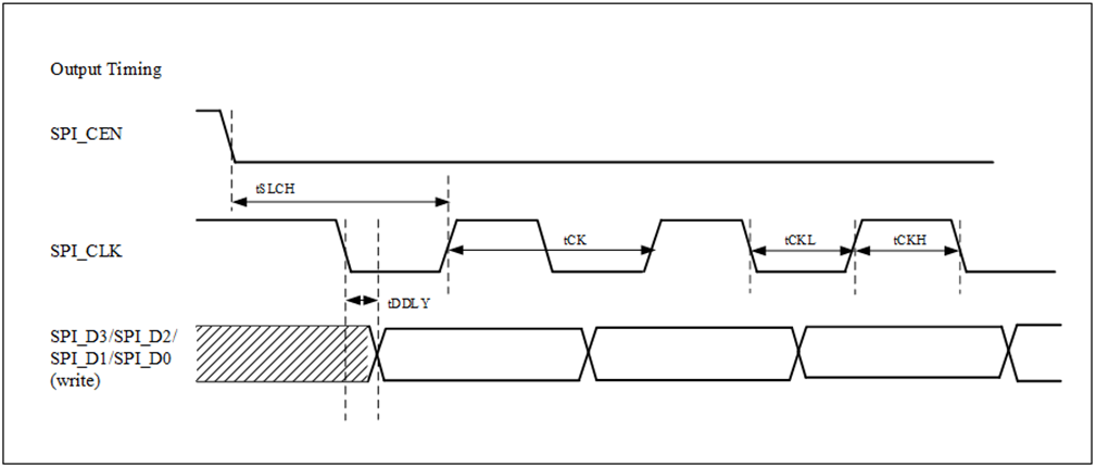
Figure 8-1 SPI NOR Output Timing
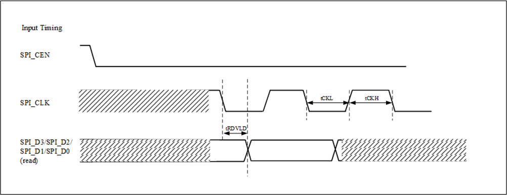
Figure 8-2 SPI NOR Input Timing
Symbol | Parameter | Conditions | Data Bit | Unit | |||
|---|---|---|---|---|---|---|---|
MIN. | Typ. | MAX. | |||||
tCK | Clock cycle for SPI NOR Flash | 9.88 | D0 | ns | |||
tCKH | Clock high-level width for SPI NOR Flash | 4.94 | D1 | ns | |||
tCKL | Clock low-level width for SPI NOR Flash | 4.94 | D2 | ns | |||
tSLCH | SPI_NOR_CEN active setup time relative to SPI_NOR_CLK | 19.76 | D3 | ns | |||
tDDLY | Write data output delay from SPI_NOR_CLK Falling edge | 0.30 | D0 | ns | |||
D1 | |||||||
D2 | |||||||
D3 | |||||||
tRDVLD | Read data valid time | 2.50 | D0 | ns | |||
D1 | |||||||
D2 | |||||||
D3 | |||||||
Note : Test for Clock cycle of SPI_NOR_FLASH device is 101.25Mhz.
8.6.2. SPI NAND FLASH Specification
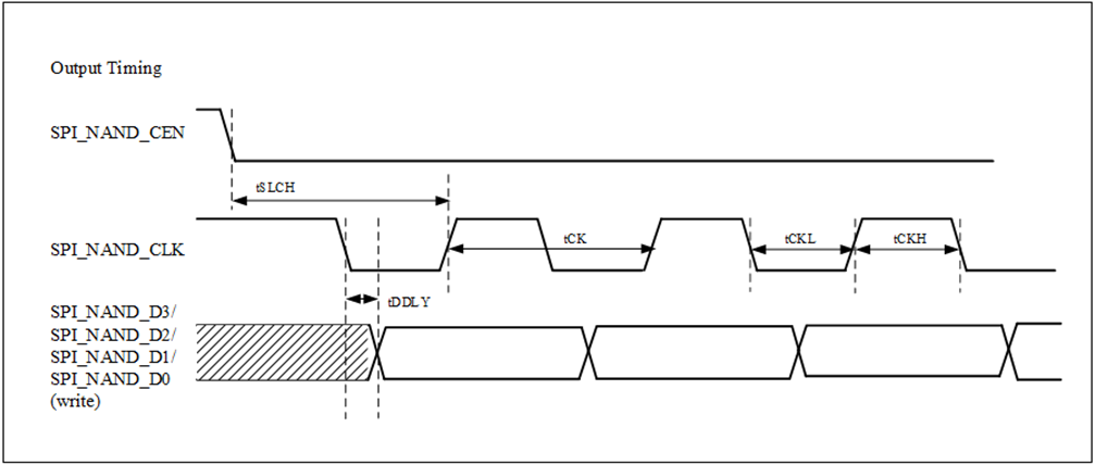
Figure 8-3 SPI NAND Output Timing
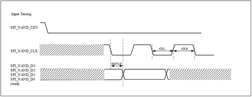
Figure 8-4 SPI NAND Input Timing
Symbol | Parameter | Conditions | Data Bit | Unit | ||
|---|---|---|---|---|---|---|
MIN. | Typ. | MAX. | ||||
tCK | Clock cycle for SPINAND | 9.88 | D0 | ns | ||
tCKH | Clock high-level width for SPI NAND | 4.94 | D1 | ns | ||
tCKL | Clock low-level width for SPI NAND | 4.94 | D2 | ns | ||
tSLCH | SPI_NAND_CEN active setup time relative To SPI_NAND_CLK | 19.76 | D3 | ns | ||
tDDLY | Write data output delay from SPI_NAND_CLK falling edge | 0.6 | D0 | ns | ||
D1 | ||||||
D2 | ||||||
D3 | ||||||
tRDVLD | Read data valid time | 3 | D0 | ns | ||
D1 | ||||||
D2 | ||||||
D3 | ||||||
8.6.3. eMMC Timing Diagrams
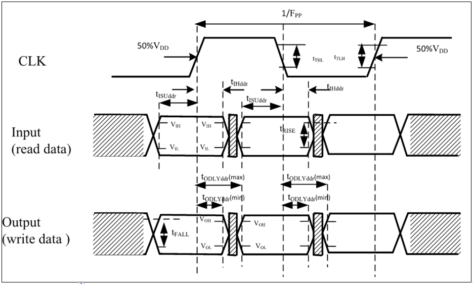
Figure 8-5 eMMC Timing
Bus Timing - Parameters Values ( High Speed ) | |||||
Clock CLK (All values are referred to min (VIH) and max (VIL)) , CL ≦ 30 pF | |||||
Parameter | Symbol | Specification | Unit | ||
Min. | Typ. | Max. | |||
Clock Frequency Data Transfer Mode | FPP | 50 | MHz | ||
Clock duty cycle | 50 | % | |||
Clock rise time | tTLH | 1.9 | 2.2 | ns | |
Clock fall time | tTHL | 2.6 | 3.3 | ns | |
Input DAT (referenced to CLK-DDR mode), CL ≦ 20 pF | |||||
Input set-up time | tISUddr | 5.1 | ns | ||
Input hold time | tIHddr | 2.8 | ns | ||
Output DAT (referenced to CLK-DDR mode), CL ≦ 20 pF | |||||
Output delay time during | tODLYddr | max :6.9 | ns | ||
Signal rise time | tRISE | 2.8 | ns | ||
Signal fall time | tFALL | 2.8 | ns | ||
Input CMD (referenced to CLK-SDR mode), CL ≦ 20 pF | |||||
Input set-up time | tISU | 13.9 | ns | ||
Input hold time | tIH | 3.5 | ns | ||
Output CMD (referenced to CLK-SDR mode), CL ≦ 20 pF | |||||
Output delay time during | tODLY | 5.9 | ns | ||
Output hold time | tOH | 3.5 | ns | ||
Signal rise time | tRISE | 2.3 | ns | ||
Signal fall time | tFALL | 2.7 | ns | ||
eMMC Interface AC timing
Push-pull Signal Level for High Voltage | ||||
Parameter | Symbol | Specification | Unit | |
Min. | Max. | |||
Supplu Voltage | VDD | 2.7 | 3.6 | V |
Output High Voltage | VOH | 3.0 | V | |
Output Low Voltage | VOL | 0.45 | V | |
Input High Voltage | VIH | 3.0 | 3.6 | V |
Input Low Voltage | VIL | 0 | 0.45 | V |
eMMC Interface signal level measurement
Bus Timing - Parameters Values ( High Speed ) | ||||
Input DAT (referenced to CLK-DDR mode), CL ≦ 20 pF | ||||
Parameter | Symbol | Specification | Unit | |
Min. | Max. | |||
Input set-up time | tISUddr | 2.0 | ns | |
Input hold time | tIHddr | 2.2 | ns | |
Output delay time during | tODLYddr (max) | 8.6 | ns | |
Output delay time during | tODLYddr (min) | 1.3 | ns | |
8.6.4. SD/SDIO Timing Diagrams
SD/SDIO High speed Mode
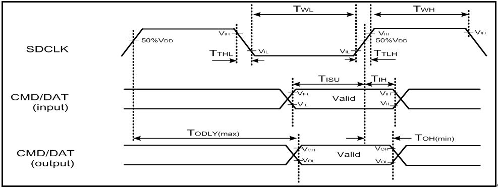
Figure 8-6 SD/SDIO Timing
Symbol | Parameter | Conditions | MIN. | Typ. | MAX. | Unit |
VDD | Supplu Voltage | 2.7 | 3.6 | V | ||
VOH | Output High Voltage | IOH = -2mA VDD min | 0.75 * VDD | V | ||
VOL | Output Low Voltage | IOL = 2mA VDD min | 0.125 * VDD | V | ||
VIH | Input High Voltage | 0.625 * VDD | VDD + 0.3 | V | ||
VIL | Input Low Voltage | VSS-0.3 | 0.25*VDD | V | ||
Power Up Time | From 0V to VDD min | 250 | ms |
Threshold Level for High Voltage
Threshold Level for High Voltage | ||||
Parameter | Symbol | Specification | Unit | |
Min. | Max. | |||
Supplu Voltage | VDD | 2.7 | 3.6 | V |
Output High Voltage | VOH | 3 | V | |
Output Low Voltage | VOL | 0.25 | V | |
Input High Voltage | VIH | 3.0 | 3.3 | V |
Input Low Voltage | VIL | 0.20 | 0.30 | V |
Power Up Time | 250ms | ns | ||
Bus Timing - Parameters Values ( High Speed ) | ||||
Clock CLK (All values are referred to min (VIH) and max (VIL)) , CCARD ≦ 10 pF ( 1 card ) | ||||
Parameter | Symbol | Specification | Unit | |
Min. | Max. | |||
Clock Frequency Data Transfer Mode | FPP | 0 | 50 | MHz |
Clock low time | TWL | 7 | ns | |
Clock high time | TWH | 7 | ns | |
Clock rise time | TTLH | 3 | ns | |
Clock fall time | TTHL | 3 | ns | |
Input CMD , DAT (referenced to CLK), CCARD ≦ 10 pF ( 1 card ) | ||||
Input set-up time | TISU | 6 | ns | |
Input hold time | TIH | 2 | ns | |
Output CMD, DAT (referenced to CLK), CCARD ≦ 40 pF ( 1 card ) | ||||
Output Delay time during | TODLY | 0 | 14 | ns |
Output Hold time | TOH | 2.5 | ns | |
Bus Timing - Parameters Values (High Speed)
8.6.5. MIPI Low Power receiver AC specification.
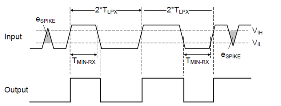
Figure 8-7 Input Glitch Rejection of Low-Power receiver
MIPI LP receiver AC specifications
Symbol | Parameter | Conditions | MIN. | Typ. | MAX. | Unit |
eSPIKE | Input pulse rejection | 300 | V*ps | |||
TMIN_RX | Minimum pulse width response | 20 | ns | |||
VINT | Peak interference amplitude | 200 | mV | |||
FINT | Interference frequency | 300 | 450 | MHz |
8.6.6. Ethernet Timing Diagrams
Serial Management Timing
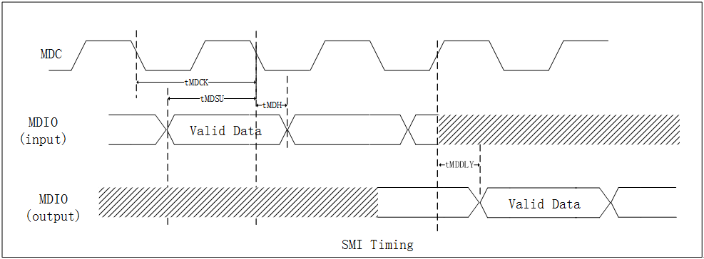
Figure 8-8 Ethernet SMI timing diagram
Symbol | Parameter | Condition | Unit | ||
MIN. | Typ. | MAX. | |||
tMDCK | Clock cycle for MDIO | 400 | ns | ||
tMDCKH | Clock high-level width for MDIO | 200 | ns | ||
tMDCKL | Clock low-level width for MDIO | 200 | ns | ||
tMDDLY | MDC to MDIO (input) Delay Time | 240 | ns | ||
tMDSU | MDIO (output) to MDC Setup Time | 10 | ns | ||
tMDH | MDIO (output) to MDC Hold Time | 10 | ns | ||
SMI AC Timing
RMII Timing
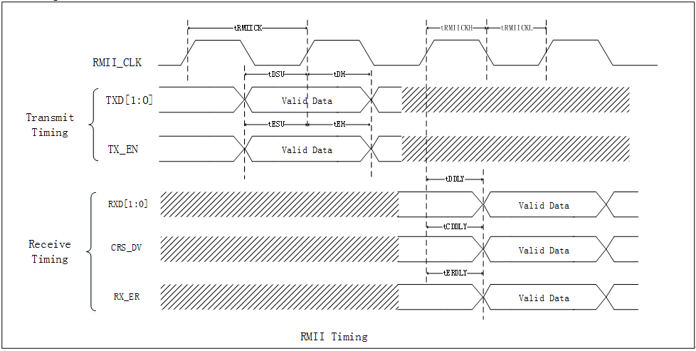
Figure 8-9 RMI timing diagram
Symbol | Parameter | Condition | Unit | ||
MIN. | Typ. | MAX. | |||
tRMIICK | RMII Clock Period | 20 | ns | ||
RMII Clock Duty Cycle | 35 | 65 | % | ||
tDSU | TX_Data Setup to RMII Clock rising | 4 | ns | ||
tDH | TX_Data Hold from RMII Clock rising | 2 | ns | ||
tESU | TX_EN Setup to RMII Clock rising | 4 | ns | ||
tEH | TX_EN Hold from RMII Clock rising | 2 | ns | ||
tDDLY | RX_Data Delay from RMII Clock rising | 4 | 10 | 14 | ns |
tCDDLY | CRS_DV Delay from RMII Clock rising | 4 | 10 | 14 | ns |
Table 1 RMII AC Timing
8.6.7. I2C AC Timing Diagram
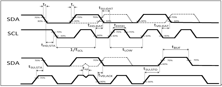
Figure 8-10 I2C AC timing diagram
SYMBOL | STANDARD-MODE | FAST-MODE | UNIT | ||
MIN. | MAX | MIN. | MAX | ||
fSCL | 0 | 100 | 0 | 400 | kHZ |
tHD;STA | 4.0 | – | 0.6 | – | μs |
tLOW | 4.7 | – | 1.3 | – | μs |
tHIGH | 4.0 | – | 0.6 | – | μs |
tSU;STA | 4.7 | – | 0.6 | – | μs |
tHD;DAT | 0 | 3.45 | 0 | 0.9 | μs |
tSU;DAT | 250 | – | 100 | – | ns |
tr | – | 1000 | 20 | 300 | ns |
tf | – | 300 | 300 | ns | |
tSU;STO | 4.0 | – | 0.6 | – | μs |
tBUF | 4.7 | – | 1.3 | – | μs |
tVD;DAT | – | 3.45[4] | – | 0.9 | μs |
tVD;ACK | – | 3.45 | – | 0.9 | μs |
tSP | – | – | 0 | 50 | ns |
I2C Timing Table.
8.6.8. I2S Master AC Timing Diagrams
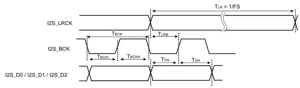
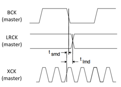
Figure 8-11 I2S (Master) AC Timing diagram
Symbol | Parameter | Condition | Unit | ||
MIN. | Typ. | MAX. | |||
TLR = 1/FS | LRCK Period (1/FS) | us | |||
FS | LRCK Frequency | KHz | |||
TBCK = 1/ FBCK | BCK Period | 32 | 192 | ns | |
FBCK | BCK Frequency | MHz | |||
TBCKL | BCK Pulse Width Low | 2.048 | 12.288 | ns | |
TBCKH | BCK Pulse Width High | 244 | ns | ||
TLRB | LRCK Edge to BCK Rising Edge | 244 | ns | ||
Tsmd | XCK to BCK active edge delay | 0 | 15 | ns | |
Timd | XCK to LRCK delay | 0 | 15 | ns | |
I2S IN (Master) AC Timing
Symbol | Parameter | Condition | Unit | ||
|---|---|---|---|---|---|
MIN. | Typ. | MAX. | |||
TLR = 1/FS | LRCK Period (1/FS) | us | |||
FS | LRCK Frequency | KHz | |||
TBCK = 1/ FBCK | BCK Period | 32 | 192 | ns | |
FBCK | BCK Frequency | MHz | |||
TBCKL | BCK Pulse Width Low | 2.048 | 12.288 | ns | |
TBCKH | BCK Pulse Width High | 244 | ns | ||
TLRB | LRCK Edge to BCK Rising Edge | 4 | 244 | ns | |
TDS | I2S_D0 Set-Up Time | 6 | ns | ||
TDH | I2S_D0 Hold Time | 6 | ns | ||
Tsmd | XCK to BCK active edge delay | 0 | 15 | ns | |
Timd | XCK to LRCK delay | 0 | 15 | ns | |
I2S OUT (Master) AC Timing