13. Universal Asynchronous Receiver Transmitter (UART)
- edwin.chiu (Unlicensed)
13.1 Universal Asynchronous Receiver Transmitter (UART)
13.1.1 Introduction
The UART is a Universal Asynchronous Receiver/Transmitter, the interface is EIA RS-232C DB-9 industry standard. The registers space locate to address 0x9C000800~0x9C0009FF and 0x9C008780~0x9C0087FF. The UART block is used to serially receive and transmit data to a peripheral device. It contains registers to control the character length, baud rate, parity check and interrupt generation. It is also equipped with FIFO controls to buffer the receive and transmit data, and to enable/disable the FIFOs. Both receive and transmit FIFO's depth are 128byte. There are UART0~4 that supported in SP7021, the features list as below.
- Support Full-duplex communication.
- Support data packet length configurable.
- Support stop bit number configurable.
- Support force break condition.
- Support baud rate configurable.
- Support error detection and report.
- Support RXD Noise Rejection Vote configurable.
The following descriptions are based on UART0. The other UART blocks have the same structure and features.
13.1.2 Function Diagram
A generalized function diagram of UART is shown in Figure 13-1.
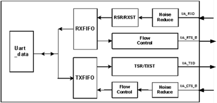
Figure 13-1 UART Functional Blocks
- UART_DATA: Used to let the CPU read and write to the FIFO through RGST.
- RXFIFO: UART_RXFIFO supports 128 byte receive data FIFOs and FIFO status, such as not empty. Users can read data from RXFIFO through accessing Group18.0 uart0_data register and check FIFO status through read Group18.1 uart0_lsr register bit1.
- TXFIFO: UART TXFIFO supports 128 byte is used to store the data written by user through Group18.0 uart0_data register, and also provides FULL and empty status and empty interrupt to user through Group18.1 uart0_lsr register, which is convenient for TXFIFO operation.
- RSR_RXST: UART's receiver state machine include the following state: IDLE_ST, START_ST, DATA0_ST, DATA1_ST, DATA2_ST, DATA3_ST, DATA4_ST, DATA5_ST, DATA6_ST, DATA7_ST, PARITY_ST, STOP0_ST, FAIL_ST. UART transform serial UA_RXD data into parallel through RSR register under the control of RXST. Then it will write the parallel RSR data into RXFIFO.
- TSR_TXST: UART's transmit state machine include the following state: IDLE_ST, START_ST, DATA0_ST, DATA1_ST, DATA2_ST, DATA3_ST, DATA4_ST, DATA5_ST, DATA6_ST, DATA7_ST, PARITY_ST, STOP0_ST, STOP1_ST. Data is transferred from TXFIFO to TSR register. TSR can transform the parallel data into serial data under the control of TXST.
- Noise Reduce: For UA_RXD, there are two levels of noise reduction. The first one is 3 times sampled with SYSCLK, only three consecutive ones will change their value to one, and for their value to be zero, three consecutive zeros must be received. This first level of noise reduction can't be disabled. The second level of noise reduction is the majority vote logic; by default this second level of noise reduction is disabled. Software can set it to 3VOTE, 5VOTE or 7VOTE. If the VOTE_SEL is set to 3VOTE, the majority for three consecutive RXD values (sampling clock is 16 x baud rate) are selected as the received RXD value. If it is set to 5VOTE, the majority for five consecutive RXD values (sampling clock is 16 x baud rate) are selected as the received RXD value. If it is set to 7VOTE, the majority for seven consecutive RXD values (sampling clock is 16 x baud rate) are selected as the received RXD value. User can control sample vote through (Group18.3 uart0_lcr[7:6]).
- Flow Control: Flow Control Block is composed on AUTO_CTS mode and AUTO_RTS mode. They can be enabled and disabled independently by programming bit6 and bit5 of Modem Control Register (Group18.4 uart0_mcr). If the AUTO_CTS mode is enabled, the TX function is disabled as long as the UA_CTS_B is high (inactive). Transmission will resume when the CTS pin return to logic 0. If the AUTO_RTS mode is enabled, the UA_RTS_B goes high (inactive) when there is only one space left in the Rx FIFO, and it returns to low (active) when the data in the Rx FIFO is less than fifteen. The Flow Control Block work with Modem mode only and the flow controlled by hardware. In the Line mode, the data transaction is only through UA_TXD and UA_RXD.
13.1.3 Serial Data Format
The UART serial data format is shown in Figure 13-2. The data sampling chart is shown in Figure 13-3.
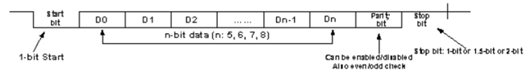
Figure 13-2 Serial Data Format
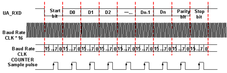
Figure 13-3 Data Sampling Chart
The data length can be selected by programming the bit [1:0] in the Group18.3 uart0_lcr register for UART0.The number of stop bits can be selected by programming the bit [2] in the Group18.3 uart0_lcr register for UART0.The parity bit enable function can be selected by programming the bit [3] in the Group18.3 uart0_lcr register for UART0.The parity bit polarity can be selected by programming the bit [4] in the Group18.3 uart0_lcr register for UART0.
13.1.4 Baud Rate Generation
The baud rate for receiver and transmitter are both set to the same value as programed in the uart0_div_l and uart0_div_h registers for UART0. The divisor0_ext [3:0] is in the bit [15:12] of Group18.5 uart0_div_l register. The divisor [7:0] is in the bit [7:0] of Group18.5 uart0_div_l register. The divisor [15:8] is in the bit [7:0] of Group18.6 uart0_div_h register. The baud rate calculation formula is shown as below.
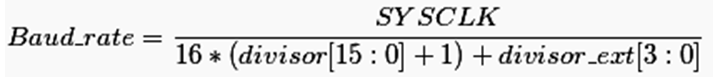
The SYSCLK can be changed fixed 27MHz by set CLK_BAUD to 1. The CLK_BAUD is bit0 of register Group18.11 uart0_clk_baud_sel.
- TXCLK Generation: When TXFIFO is not empty, UART will start data transfer. When TXST jumps into START_ST from IDLE, it will load data to TX_DIV_EXT from DIVISOR_EXT. TX_DIV_EXT will be change from the loaded value to 0, then load data from DIVISOR to TXCNT. (TXCNT will count from loaded data to 0, and then do the same countering for 15 times). Time duration of all the process is equal to baud rate time, which is programmed by the users. The TXCLK will pull up one cycle (a UART_CLK cycle) at this time. For the generation mechanism of TXCLK, please refer to the figure 13-4.
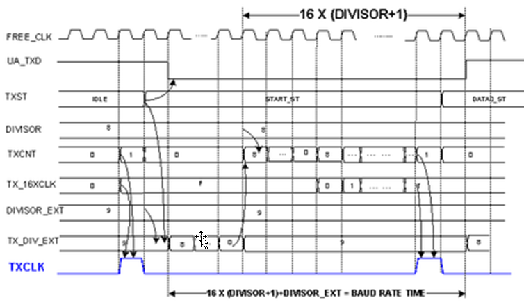
Figure 13-4 TXCLK Generation Mechanism
- RXCLK Generation: UART transform serial UA_RXD data into RXFIFO through RSR register under the control of RXST. When RXST jumps into START_ST from IDLE, it will write data to RX_DIV_EXT from DIVISOR_EXT. RX_DIV_EXT will be change from the loaded value to 0, then load data from DIVISOR to RXCNT. (RXCNT will count from loaded data to 0, and then do the same countering for 15 times). Time duration of all the process is equal to baud rate time, which is programmed by the users. The RXCLK will pull up one cycle (a UART_CLK cycle) at this time. For the generation mechanism of RXCLK, please refer to the figure 13-5.
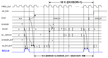
Figure 13-5 RXCLK Generation Mechanism
Error calculation for programmed baud rates at SYSTEMCLK=202MHz and oversampling by 16: Please refer to table 13-1
SYSCLK
202MHZ
Baud rate(ideal)
Over sampling
Divisor
Divisor_ext
Error(%)
Baud rate(real)
115200
16
109
9
0.026
115231
230400
16
54
13
0.03
230330
460800
16
27
7
0.14
460136
921600
16
13
12
0.3
918181
1843200
8
13
6
0.3
1836363
Table 13-1 Error calculation with baud rate
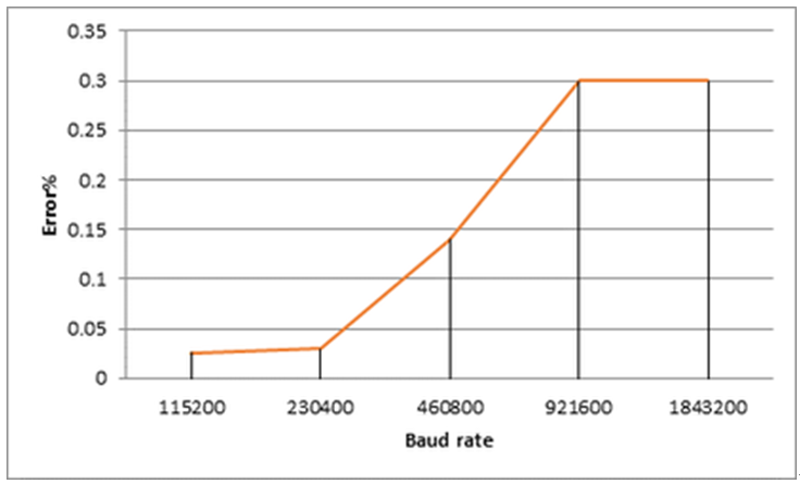
Figure 13-6 Error calculation with baud rate
Please notice that Error rate should under 3% when programmed baud rate.
- Tolerance of the UART receiver to clock deviation
The UART receiver must match Fe7 ≦9% ,Fep≦10%且Be ≦4.5% condition. Please refer to figure 13-7&13-8. Fe7 is Frame error of the data bit7 (D7). Fep is Frame error of the STOP bit. Be is Bit error. Ts is the bit clock time difference between idea baud rate and slower baud rate. Tf is the bit clock time difference between idea baud rate and faster baud rate. Ti is idea baud rate bit clock time. Ideal means standard UART pulse. Slower means clock slower case UART pulse. Faster means clock faster case UART pulse.
- The Fe7 & Fep calculation: Ti7 and Tip is equal in the Ideal UART pulse case.
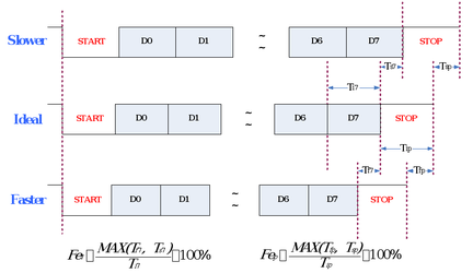
Figure 13-7 Frame error calculation
- The Be calculation: Bx include Start, Data and Stop bit.
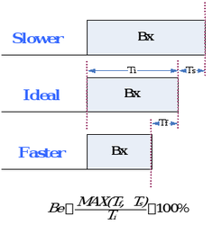
Figure 13-8 Bit error calculation
13.1.5 Parity Control
The parity control (generation of parity bit in transmission and parity checking in reception) can be enabled by set the PE bit to 1 in the bit3 of Group18.3 uart0_lcr register.
- Even parity: Even parity can be selected by set the PR bit to 1 in the bit4 of Group18.3 uart0_lcr register. The parity bit is calculated to obtain an even number of "1s" inside the frame and the parity bit. For example, data=00111111; 6 bits set parity bit will be 0 if even parity is selected.
- Odd parity: Odd parity can be selected by set the PR bit to 0 in the bit4 of Group18.3 uart0_lcr register. The parity bit is calculated to obtain an odd number of "1s" inside the frame and the parity bit. For example, data=00111111; 6 bits set parity bit will be 1 if odd parity is selected.
- Parity checking in reception: If the parity check fails, the PE flag is set in the bit2 of Group18.1 uart0_lsr register and an interrupt is generated if LSM is set to 1 in the bit6 of Group18.7 uart0_isc. An interrupt flag LS can be got in the bit2 of Group18.7 uart0_isc.
13.1.6 UART Interrupts
The UART interrupt events are connected to the same interrupt vector, please refer to figure 13-6. These events generate an interrupt if the corresponding "Enable Control Bit" is set. !worddavcc8ac9771c793b4db11c7e8d5897cc96.png|height=250,width=490!Figure 13-6 UART Interrupt Tree
The following descriptions are based on UART0.
- Modem Status IRQ: When modem status interrupt is enabled (Group18.7 uart0_isc[7]=1) and modem control signals TERI, DDCD, DCTS, DDSR (Group18.2 uart0_msr[7:4]) are set to 1, the modem status interrupt will occur. User can confirm the interrupt type through the register (Group18.7 uart0_isc[3] ). When read modem status register (Group18.2 uart0_msr[7:4]), modem status register will be cleared to 0, and modem status interrupt flag is cleared to 0 also.
- Line Status IRQ: Line status interrupt is enabled (Group18.7 uart0_isc[6]=1). If any condition of break condition (BC), frame error (FE), overrun (OE), parity error (PE) (Group18.1 uart0_lsr[5:2]) occurs in UART's controller, it will cause line status interrupt occur. The interrupt type can be confirmed by read the register (Group18.7 uart0_isc[2]). The interrupt caused by OE requires only read line status register, OE will be cleared to 0, and line status interrupt flag will be cleared to 0 too. The interrupt caused by PE, BC, and FE needs to read the uart0_data register, the next data PE, BC, and FE status reload to the current PE, BC, and FE status register. If there is no PE, BC, or FE error in the next data, PE, BC, and FE will be cleared, and the line status interrupt flag will be cleared also
- RXFIFO not empty IRQ: The size of the RXFIFO is 128 bytes. If the RX interrupt is enabled (Group18.7 uart0_isc[5]=1), the RXFIFO will immediately make UA_INT to 1 as long as there is data, so the CPU knows that a UART interrupt has occurred. The software determines the type of interrupt generated by querying Group18.7 uart0_isc[1], and the software reads the data in the FIFO through the uart0_data register. When RXFIFO is empty, the interrupt flag will be cleared to 0.
- TXFIFO empty IRQ: The size of the TXFIFO is 128 bytes. If the TX interrupt is enabled (Group18.7 uart0_isc[4]=1) and the TXFIFO is empty, the controller immediately sets UA_INT to 1, letting the CPU know that a UART interrupt has occurred. The software determines the type of interrupt generated by querying Group18.7 uart0_isc[0], and the software continues to write data to the FIFO through the uart0_data register. When TXFIFO is not empty, the interrupt flag will be cleared to 0.
13.2 UARTRX DMA (UADMA)
13.2.1 Introduction
UARTRX DMA (or named UADMA) which is used as a bridge for storing UART RX data in DRAM. The purpose is to improve CPU processing efficiency for slow peripherals. It can choose the UART0~UART4 by register setting.
There have two UADMA mechanisms that can serve each UART RX independently but can't serve the same UART at the same time.
The control registers memory map address locate at 0x9C008980-0x9C0089FF.
13.2.2 Function Diagram
UART RX circuit receives data from external device, than it issues an interrupt when the FIFO is almost full. Register bus provides the access interface for UART drive . A generalized function diagram of UADMA is shown in Figure 13-7.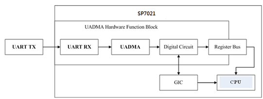
Figure 13-7 UADMA Function Diagram
13.2.3 UADMA Interrupt Handler
An interrupt is issued when UART RX data out of timeout or DMA space less than threshold. Software needs to process interrupt and copy data from DMA space to UART buffer then clear status and set DMA_GO when FIFO almost Full happened.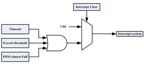
Figure 13-8 UADMA Interrupt Tree
13.3 UARTTX DMA (HW_BUF_UA)
13.3.1 Introduction
UARTTX DMA (or named HW_BUF_UA) which is used as a bridge for transfer data from DRAM to UART TX port. The purpose is to improve CPU processing efficiency for slow peripherals. It can choose the UART0~UART4 by register setting.
HW_BUF_UA construct by GDMA(General DMA Function) and UART. It can transfer data automatically with no CPU control, instead by DMA_Controller. When data size larger than 64Byte or timeout happened, the data will be catch out automatically.
According to HW_BUF_UA status is empty or full, the controller will stop or start transfer data.
There have two UARTTX DMA mechanisms that can serve each UART TX independently but can't serve the same UART at the same time.
The HW_BUF_UA control registers memory map address locate at 0x9C008A00-0x9C008A7F.
The GDMA0 control registers memory map address locate at 0x9C008880-0x9C0088FF.
The GDMA1 control registers memory map address locate at 0x9C008900-0x9C00897F.
13.3.2 Function Diagram
The block diagram of UART TX circuit is shown in Figure 13-9.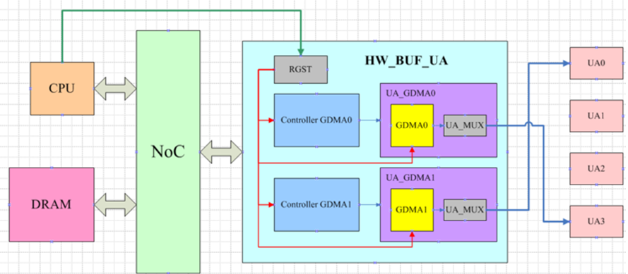
Figure 13-9 UARTTX Block Diagram
DRAM is read by GDMA through NoC, while GDMA2UART is used for data transmission through the communication protocol between GDMA and UART.
UART to the outside is transmitted via UART protocol, through TXD/RXD.
When CPU write data to DRAM, it only need update WR_ADR, Control_GDMA will auto judge the data size larger than 64Byte or timeout happened and execute DMA action.
13.3.3 Data Control Flow
- When the CPU starts to throw the debug message to the DRAM, it will first read the RD_ADR (and FULL/EMPTY) of HW_BUF_UA to ensure that the current Buffer has enough space for writing.
- After step1 is completed, the CPU will update the WR_ADR of HW_BUF_UA and notify HW_BUF_UA where the current valid data is written to.
- Control GDMA will calculate whether the Buffer is greater than or equal to 64B, if so, start GDMA to read the DRAM; otherwise, continue to wait, if no new data is written before TIMEOUT, start GDMA directly.
- The register of HW_BUF_UA can set which UART to rd/wr, if GDMA0 is selected to UART3 for rd action, the data on DRAM will be transmitted to UART through GDMA.
- Interrupt part is GDMA internal Interrupt: THRESHOLD_INT, ERROR_INT, GDMA_DONE.
13.3.4 UARTTX DMA Interrupt Handler
DEBUG mode (DEBUG_ENABLE=1, GDMA_ENABLE=1)
Only TX path
- When GDMA generates ERROR_INT, it will stop the action with the IP, and only complete the operation on the BUS (not let the BUS die).
- After step1 is over, HW_BUF_UA will send ERROR_INT to UART. After UART receives it, in order to ensure that all the previous operation data is written out, it needs to wait until TXFIFO empty to send ERROR_INT to CPU.
- CPU receives ERROR_INT and needs to perform SW_RESET action (TXFIFO_FLUSH) on UART, and then perform SW_RESET on GDMA through UART.
- If ERROR_INT is caused by TIMEOUT, you need to adjust the TIMEROUT value or other actions through the CPU.
- After all settings are completed, the CPU needs to check the cmd of REDO_CONTROLLER_DMA under HW_BUF_UA.
Normal mode (DEBUG_ENABLE=0, GDMA_ENABLE=1)
TX path
- After the CPU sets UART_SELECT_RD and GDMA, etc., GDMA will start to read data from DRAM to UART.
- The GDMA error interrupt that will be used has TIMEOUT_INT.
- Error Interrupt flow is the same as debug mode, UART needs to ensure that all data has been transmitted.
- But there is no need to download REDO_CONTROLLER_DMA, because the debug mode is no longer at this time, just reset the CPU.
RX path
- After the CPU sets UART_SELECT_WR and GDMA, etc., GDMA will start to capture data and write into DRAM through UART.
- The GDMA error interrupt that will be used has TIMEOUT_INT / WRITE_INT.
- When an error interrupt occurs, GDMA will directly cut off the communication with the UART to ensure that the transmission on the BUS ends correctly, and then send an error interrupt to the UART.
- At this time, the UART will immediately transmit the error interrupt to the CPU, and the CPU will perform SW_RESET on the UART, and then perform SW_RESET on the GDMA.
- After GDMA SW_RESET_DONE, the CPU can start to set.
13.4 Registers Map
13.4.1 Register Memory Map
UART Register Memory Map
Group Base Address | Data Width | Group No. | Module |
0x9C000800 | 32 | 16 | UA2 (UART2) |
0x9C000880 | 32 | 17 | UA3 (UART3) |
0x9C000900 | 32 | 18 | UA0 (UART0) |
0x9C000980 | 32 | 19 | UA1 (UART1) |
0x9C008780 | 32 | 271 | UA4 (UART4) |
0x9C008880 | 32 | 273 | HWUA_GDMA0 |
0x9C008900 | 32 | 274 | HWUA_GDMA1 |
0x9C008980 | 32 | 275 | UARTRX DMA (UADMA) |
0x9C008A00 | 32 | 276 | UARTTX DMA (HW_BUF_UA) |
Table 13-2 UART Register Memory Map
All UARTs' registers have the same offset (address - base address) in corresponding UART register group. Only UART2 and UART DMA registers are described in following register description, for other UARTs (UART0, 1, 3, 4) please refer to UART2 description for more detail.
13.4 .2 Registers Description
UART Register Description
RGST Table Group 16 UART2
16.0 UART2 Data Port Register (uart2 data)
Address: 0x9C000800
Reset: 0x0000
Field Name | Bit | Access | Description |
RSV | 15:8 | RO | Reserved |
UD | 7:0 | RW | UART DATA UART2 data transmit/receive FIFO port.Write to this register will store the written data to the output (TX) FIFO, |
16.1 UART2 Line Status Register (uart2 lsr)
Address:0x9C000804
Reset:0x0041
Field Name | Bit | Access | Description |
RSV | 15:8 | RO | Reserved |
TXE | 6 | RO | Transmit FIFO is Empty 0: Transmit FIFO is not empty. 1: Transmit-ended, transmit FIFO is empty. |
BC | 5 | RO | Break Condition 0: No break condition. 1: A break condition occurs and associated byte is 00. |
FE | 4 | RO | Frame Error 0: No frame error. 1: Frame error of current reading data. |
OE | 3 | RO | Overrun Error 0: No overrun error since last read. 1: Overrun error occurs (clear upon read). |
PE | 2 | RO | Parity Error 0: No Parity error. 1: Parity error occurs at current reading data. |
RX | 1 | RO | Receive FIFO status 0: Receive FIFO is empty. 1: Receive FIFO not empty. |
TX | 0 | RO | Transmit FIFO status 0: Transmit FIFO is full. 1: Transmit FIFO is not full (and available for more input). |
16.2 Modem Status Register (uart2 msr)
Address: 0x9C000808
Reset: 0x007f
Field Name | Bit | Access | Description |
RSV | 15:8 | RO | Reserved |
TE RI | 7 | RC | Trailing edge of Ring indicator 0: No Change. 1: Set when input RI B has changed from low to high state. |
DT DCD | 6 | RC | Delta data carrie detect indicator 0: No Change. 1: Set when input DCD B has changed state. |
DT CTS | 5 | RC | Delta clear to send indicator 0: No Change. 1: Set when input CTS B has changed state. |
DT DSR | 4 | RC | Delta clear to send indicator 0: No Change. 1: Set when input DSR B has changed state. |
RI | 3 | RO | RI indicator Disable loop back mode, RI is the inverse of input port RI B. Enable loop back mode, RI is connected to bit 3 of MCR register. |
DCD | 2 | RO | Data carrier detect Disable loop back mode, DCD is the inverse of input port DCD B. Enable loop back mode, DCD is connected to bit 2 of MCR register. |
CTS | 1 | RO | Clear to send Disable loop back mode, CTS is the inverse of input port CTS B. Enable loop back mode, CTS is connected to RTS internally. |
DSR | 0 | RO | Data to ready Disable loop back mode, DSR is the inverse of input port DSR B. Enable loop back mode, DSR is connected to DTR internally. |
16.3 UART2 Line-Control Register (uart2 lcr)
Address: 0x9C00080C
Reset: 0x0003
Field Name | Bit | Access | Description |
RSV | 15:8 | RO | Reserved |
Vote | 7:6 | RW | Vote select (RXD noise rejection) 0x0: No major vote on uart2 RXD(default). 0x1: 3-sample vote. 0x2: 5-sample vote. 0x3: 7-sample vote. |
BC | 5 | RW | Break condition select (START BIT) 0: No break condition(default). 1: Force serial output to spacing (low) state, break condition. |
RP | 4 | RW | Parity bit polarity select 0: Odd parity(default). 1: Even parity. |
PE | 3 | RW | Parity bit enable 0: Disable parity bit(default). 1: Enable parity bit. |
ST | 2 | RW | Number of stop bits 0: 1 stop bit(default). 1: For word length=5, 1.5 stop bits, for word length > 5, 2 stop bits. |
WL | 1:0 | RW | Word length 0x0: 5bit. 0x1: 6bit. 0x2: 7bit. 0x3: 8bit(default). |
16.4 UART2 Modem Control Register (uart2 mcr)
Address: 0x9C000810
Reset: 0x0000
Field Name | Bit | Access | Description |
RSV | 15:8 | RO | Reserved |
AT | 7 | RW | AUTO CALIBRATE 0: No auto calibrate (or auto-calibration finished)(default). 1: Start baud-rate auto calibration. Calibration will stop after receive expected token (ASCII 'a' or 'A'). |
AC | 6 | RW | AUTO CTS mode 0: Disable CTS detection, TX FIFO sends out data always(default). 1: Enable CTS detection, only send data when CTS B is active (low). |
AR | 5 | RW | AUTO RTS mode 0: UART RTS B is controlled by RTS register(default). 1: UART RTS B is controlled by receive FIFO status. |
LB | 4 | RW | MCR loop-back mode 0: Disable loop-back (normal function)(default). 1: Loop-back mode. |
RI | 3 | RW | Ring-indicator register 0: UART RI inactive (output low)(default). 1: UART RI active (output high). |
DCD | 2 | RW | Data carrier detect register 0: UART DCD B inactive (output high)(default). 1: UART DCD B active (output low). |
RTS | 1 | RW | Request to send register (not used in AUTORTS mode) 0: UART RTS B inactive (output high)(default). 1: UART RTS B active (output low). |
DTS | 0 | RW | Data terminal ready register 0: UART DTR B inactive (output high)(default). 1: UART DTR B active (output low). |
16.5 UART2 Clock Divider Low Register (uart2 div l)
Address: 0x9C000814
Reset: 0x903A
UART2 clock divisor for 16x over-sampling clock (low part)
Field Name | Bit | Access | Description |
divisor ext[3:0] | 15:12 | RW | Extension of divisor[] see divisor[7:0]. |
RSV | 11:8 | RO | Reserved |
divisor[7:0] | 7:0 | RW | System clock divisor LSB |
16.6 UART2 Clock Divider High Register (uart2 div h)
Address: 0x9C000818
Reset: 0x0000
Field Name | Bit | Access | Description |
RSV | 15:8 | RO | Reserved |
divisor[15:8] | 7:0 | RW | System clock divisor MSB |
16.7 UART2 Interrupt Status/Control register (uart2 isc)
Address: 0x9C00081C
Reset: 0x0000
Field Name | Bit | Access | Description |
RSV | 15:8 | RO | Reserved |
MSM | 7 | RW | Modem Status interrupt Mask 0: INT disable(default). 1: INT enable. |
LSM | 6 | RW | Line Status interrupt Mask 0: INT disable(default). 1: INT enable. |
RXM | 5 | RW | RX interrupt Mask 0: INT disable(default). 1: INT enable. |
TXM | 4 | RW | TX interrupt Mask 0: INT disable(default). 1: INT enable. |
MS | 3 | RU | Modem status interrupt flag This bit is set when any of DT DSR, DT CTS, DT DCD, or TE RI is one and MSR interrupt is enabled. 0: No modem status interrupt issued(default). 1: Modem status interrupt issued. |
LS | 2 | RU | Line status interrupt flag This bit is asserted when and of PE, FE, BC, OE condition occurred and LS interrupt is enable. 0: No line status interrupt issued(default). 1: Line status interrupt issued. |
RX INT | 1 | RU | RX FIFO NOT EMPTY interrupt flag. This bit is asserted when RX FIFO is not empty and RX interrupt enable. 0: No RX interrupt issued(default). 1: RX interrupt issued. |
TX INT | 0 | RU | TX FIFO EMPTY interrupt flag. |
16.8 UART2 TX Residue (uart2 tx residue)
Address: 0x9C000820
Reset: 0x0000
Field Name | Bit | Access | Description |
RSV | 15:7 | RO | Reserved |
tx residue | 6:0 | RO | tx residue, TX FIFO flush Read to get the remainder characters in the TX FIFO. |
16.9 UART2 RX Residue (uart2 rx residue)
Address: 0x9C000824
Reset: 0x0000
Field Name | Bit | Access | Description |
RSV | 15:7 | RO | Reserved |
rx residue | 6:0 | RO | rx residue, RX FIFO flush Read to get the remainder characters in the RX FIFO. |
16.10 UART2 RX FIFO Threshold (uart2 rx threshold)
Address: 0x9C000828
Reset: 0x0000
Field Name | Bit | Access | Description |
RSV | 15:12 | RO | Reserved |
RXFIFO THRESHOLD | 11:4 | RW | RXFIFO Threshold Value Set the remainder space in the RXFIFO. If the remaining space is less than RXFIFO THRESHOLD, it would assert interrupt when RXFIFO Threshold is enabled. unit : byte. |
RSV | 3:1 | RO | Reserved |
RXFIFO THR ENABLE | 0 | RW | RXFIFO Threshold Enable 0 : disable threshold control for RXFIFO(default). 1 : enable threshold control for RXFIFO. |
16.11 UART2 clock baud rate select (uart2 clk baud sel)
Address: 0x9C00082C
Reset: 0x0001
Field Name | Bit | Access | Description |
RSV | 15:1 | RO | Reserved |
CLK BAUD | 0 | RW | UART CLK BAUD RATE SEL 0 : select to SYSCLK. 1 : 27MHz (default). |
RGST Table Group 17 UART3 (Base Address: 0x9C000880, Please refer to UART2 register offset and description for more detail)
RGST Table Group 18 UART0 (Base Address: 0x9C000900, Please refer to UART2 register offset and description for more detail)
RGST Table Group 19 UART1 (Base Address: 0x9C000980, Please refer to UART2 register offset and description for more detail)
RGST Table Group 271 UART4 (Base Address: 0x9C008780, Please refer to UART2 register offset and description for more detail)
RGST Table Group 273 GDMA: General DMA (HWUA_GDMA0)
273.0 DMA HW VER (dma hw ver)
Address: 0x9C008880
Reset: 0x0179 1000
Field Name | Bit | Access | Description |
DMA HW VER | 31:0 | RO | Hardware Version A constant, usually stands for hw delivery date, such as 32'h01791000. |
273.1 DMA CONFIG (dma config)
Address: 0x9C008884
Reset: 0x0000 0004
Field Name | Bit | Access | Description |
Reserved | 31:9 | RO | Reserved |
DMA GO | 8 | RUW | DMA GO Signal Write 1 to trigger DMA hardware, self clear to zero when current operation has been finished. |
Reserved | 7:3 | RO | Reserved |
NON BUF MODE | 2 | RW | GDMA write command bufferable |
SAME SLAVE | 1 | RW | GDMA access same slave |
DMA MODE | 0 | RW | Set DMA Mode |
273.2 DMA LENGTH (dma length)
Address: 0x9C008888
Reset: 0x0000 0000
Field Name | Bit | Access | Description |
Reserved | 31:25 | RO | Reserved |
DMA LENGTH | 24:0 | RW | Set DMA Length DMA read and write function support length. |
273.3 DMA ADR (dma adr)
Address: 0x9C00888C
Reset: 0x0000 0000
Field Name | Bit | Access | Description |
DMA SRC ADR | 31:0 | RW | DMA Source Address |
273.4 DMA PORT MUX (dma port mux)
Address: 0x9C008890
Reset: 0x0000 0000
Field Name | Bit | Access | Description |
Reserved | 31:1 | RO | Reserved |
PORT MUX | 0 | RW | PORT MUX |
273.5 DMA INT FLAG (dma int flag)
Address: 0x9C008894
Reset: 0x0000 0000
Field Name | Bit | Access | Description |
Reserved | 31:7 | RO | Reserved |
LENGTH0 REG | 6 | W1C | Length is zero flag |
THRESHOLD REG | 5 | W1C | Threshold flag |
IP TIMEOUT REG | 4 | W1C | Peripheral IP Timeout When GDMA wait Peripheral IP too long, this bit will be set to HIGH. Depend on IP_TIMEOUT_DEF_WRITE and IP_TIMEOUT_DEF_READ. |
GDMA TIMEOUT REG | 3 | W1C | GDMA Timeout When Peripheral IP wait GDMA too long will set HIGH, depend on GDMA_TIMEOUT_DEF_WRITE and GDMA_TIMEOUT_DEF_READ. |
WRITE BYTE ENABLE ERROR REG | 2 | W1C | Peripheral IP WRITE_BYTE_EN error flag WRITE_BYTE_EN not meet the protocol. |
WRITE CNT | 1 | W1C | Peripheral IP DATA CNT error flag Data Count error. |
DMA DONE FLAG | 0 | W1C | DMA DONE If DMA done, this bit will be assert. Write 1 to clear. |
273.6 DMA INT EN (dma int en)
Address: 0x9C008898
Reset: 0x0000 0041
Field Name | Bit | Access | Description |
Reserved | 31:7 | RO | Reserved |
LENGTH0 EN | 6 | RW | LENGTH0 Interrupt Enable |
| THRESHOLD EN | 5 | RW | THRESHOLD Interrupt Enable |
| IP TIMEOUT EN | 4 | RW | IP TIMEOUT Interrupt Enable Write 1 to enable IP_TIMEOUT interrupt function. |
| GDMA TIMEOUT EN | 3 | RW | GDMA TIMEOUT Interrupt Enable Write 1 to enable GDMA_TIMEOUT interrupt function. |
| WRITE BYTE ENABLE ERROR EN | 2 | RW | Write Byte ERROR Interrupt Enable Write 1 to enable WRITE_BYTE_ENABLE_ERROR interrupt function. |
| WRITE CNT ERROR EN | 1 | RW | Write CNT ERROR Interrupt Enable Write 1 to enable WRITE_CNT_ERROR interrupt function. |
| DMA DONE EN | 0 | RW | DMA DONE Interrupt Enable Write 1 to enable DMA_DONE interrupt function. |
273.7 SW_RESET_STATE (software reset state)
Address: 0x9C00889C
Reset: 0x0000 0001
Field Name | Bit | Access | Description |
Reserved | 31:1 | RO | Reserved |
SW RESET DONE | 0 | RO | Identify SW_RESET state 0x1: reset done, ready for SW_RESET. |
273.8 Reserved (reserved)
Address: 0x9C0088A0
Reset: 0x0000 0000
Field Name | Bit | Access | Description |
Reserved | 31:0 | RO | Reserved |
273.9 Reserved (reserved)
Address: 0x9C0088A4
Reset: 0x0000 0000
Field Name | Bit | Access | Description |
Reserved | 31:0 | RO | Reserved |
273.10 SG_DMA_INDEX (sg_dma_index)
Address: 0x9C0088A8
Reset: 0x0000 0000
Field Name | Bit | Access | Description |
Reserved | 31:13 | RO | Reserved |
SG LLI RUN INDEX | 12:8 | RW | The stare LLI index in a task |
| Reserved | 7:5 | RO | Reserved |
| SG LLI ACCESS INDEX | 4:0 | RW | Index for LLI access Determine which LLI mapping to REG 0x0B 0x0F. |
273.11 SG_DMA_CONFIG (sg_dma_config)
Address: 0x9C0088AC
Reset: 0x0000 0000
Field Name | Bit | Access | Description |
Reserved | 31:3 | RO | Reserved |
SG LAST LLI IN TASK | 2 | RW | Last LLI in a task flag for LLI 1: When this LLI finish, SGDMA stop. |
| Reserved | 1 | RO | Reserved |
| DMA MODE | 0 | RW | Set DMA Mode for LLI 1: DMA_READ (read data from main memory to Peripheral IP) |
273.12 SG_DMA_LENGTH (sg_dma_length)
Address: 0x9C0088B0
Reset: 0x0000 0000
Field Name | Bit | Access | Description |
Reserved | 31:25 | RO | Reserved |
SG DMA LENGTH | 24:0 | RW | Set DMA Length for LLI DMA read and write function support length from 1bytes to 64Kbytes. Valid when DMA_GO is set to 1 and can't be changed when DMA_GO assert. |
273.13 SG_DMA_ADR (sg_dma_adr)
Address: 0x9C0088B4
Reset: 0x0000 0000
Field Name | Bit | Access | Description |
SG DMA ADR | 31:0 | RW | DMA address for LLI |
273.14 Reserved (reserved)
Address: 0x9C0088B8
Reset: 0x0000 0000
Field Name | Bit | Access | Description |
Reserved | 31:0 | RO | Reserved |
273.15 SG_SETTING (sg_setting)
Address: 0x9C0088BC
Reset: 0x0000 0000
Field Name | Bit | Access | Description |
SG DMA ENABLE | 31 | RW | SG DMA ENABLE |
| Reserved | 30:1 | RO | Reserved |
| SG DMA GO | 0 | RW | SG DMA GO Set SG_DMA_GO enable for LLI. |
273.16 THRESHOLD (threshold_parameter)
Address: 0x9C0088C0
Reset: 0x0000 0000
Field Name | Bit | Access | Description |
THRESHOLD LLI INDEX | 31:27 | RW | THRESHOLD LLI INDEX |
| Reserved | 26:25 | RO | Reserved |
| THRESHOLD LEN | 24:0 | RW | THRESHOLD LENGTH Determine the length to trigger THRESHOLD INTERRUPT. |
273.17 Reserved (reserved)
Address: 0x9C0088C4
Reset: 0x0000 0000
Field Name | Bit | Access | Description |
Reserved | 31:0 | RO | Reserved |
273.18 GDMA_READ_TIMEOUT (gdma_read_timeout setting)
Address: 0x9C0088C8
Reset: 0x0000 0000
Field Name | Bit | Access | Description |
GDMA READ TIMEOUT | 31:0 | RW | GDMA READ TIMEOUT DEFINE |
273.19 GDMA_WRITE_TIMEOUT (gdma_write_timeout setting)
Address: 0x9C0088CC
Reset: 0x0000 0000
Field Name | Bit | Access | Description |
GDMA WRITE TIMEOUT | 31:0 | RW | GDMA WRITE TIMEOUT DEFINE |
273.20 IP_READ_TIMEOUT (ip_read_timeout setting)
Address: 0x9C0088D0
Reset: 0x0000 0000
Field Name | Bit | Access | Description |
IP READ TIMEOUT | 31:0 | RW | IP READ TIMEOUT DEFINE |
273.21 IP_WRITE_TIMEOUT (ip_write_timeout setting)
Address: 0x9C0088D4
Reset: 0x0000 0000
Field Name | Bit | Access | Description |
IP WRITE TIMEOUT | 31:0 | RW | IPWRITE TIMEOUT DEFINE |
273.22 WRITE_CNT_DEBUG information (write_cnt_debug)
Address: 0x9C0088D8
Reset: 0x0000 0000
Field Name | Bit | Access | Description |
| Reserverd | 31 | RO | Reserved |
WRITE CNT DEBUG | 30:0 | RO | WRITE_CNT_DEBUG |
273.23 WRITE_BYTE_ENABLE_DEBUG information (write_byte_enable_debug)
Address: 0x9C0088DC
Reset: 0x0000 0000
Field Name | Bit | Access | Description |
| Reserverd | 31:1 | RO | Reserved |
W_BYTE_EN_DEBUG | 0 | RO | WRITE_BYTE_ENABLE_DEBUG |
273.24 SW_RESET_WRITE_CNT_DEBUG information (sw_reset_write_cnt_debug)
Address: 0x9C0088E0
Reset: 0x0000 0000
Field Name | Bit | Access | Description |
| Reserverd | 31:30 | RO | Reserved |
SW_RESET_WRITE_CNT_DEBUG | 29:0 | RO | SW _RESET WRITE CNT DEBUG |
RGST Table Group 274 GDMA: General DMA (HWUA_GDMA1) (Base Address: 0x9C008900, Please refer to HWUA_GDMA0 register offset and description for more detail)
RGST Table Group 275 UADMA
275.0 RF DMA0 ENABLE SEL (rf dma0 enable sel)
Address: 0x9C008980
Reset: 0x0000 0000
Field Name | Bit | Access | Description |
D0INT | 31 | RU | DMA0 INT 0: Clear by DMA INT CLR(default). 1: Clear INT State,DMA STATE wait for DMA GO. |
RSV | 30:21 | RO | Reserved |
D0OFC | 20 | RW | DMA0 OVER FLOW CONFIG judge the fifo threshold, stop the dma access or not when interrupt is occur. |
RSV | 19 | RO | Reserved |
D0MI | 18:12 | RW | DMA0 MSI ID DMA0 setting MSI ID. |
RSV | 11 | RO | Reserved |
D0SU | 10:8 | RW | DMA0 SELECT UART DMA0 select UA# RN, # is from 0 to 5. |
D0SRB | 7 | RW | DMA0 SOFT RESET. 0: active reset and back to initial-DMA.
a. UADMA AUTO ENABLE == 0. b. When DMA DEBUG INFO == c_dma_stage[3:0] is 0. c. Set DMA SW RSTB == 0 - 1. d. initial UADMA state. 1: normal work(default). |
D0INIT | 6 | RW | DMA0 INITIAL BEFORE DMA FIRST GO, It NEED SETTING INITIAL SETTING. 0: DMA not initial(default). 1: DMA INIT, write 1 to initialize DMA and followed by writing 0 to finish initialization. After initializedDMA WR ADDR[31:0]==DMA START ADDR[31:0] |
D0GO | 5 | RU | DMA0 GO 0: it will return to 0 automatically after triggered to 1(default). 1: DMA continue/start |
D0AE | 4 | RW | DMA0 AUTO ENABLE 0: Disable DMA0 Engine(default). 1: Enable DMA0 Engine. |
D0TIE | 3 | RW | DMA0 TIMEOUT INT EN 0: time out no issue interrupt(default). 1: time out issue interrupt. |
D0PSD | 2 | RW | DMA0 P SAFE DISABLE 0: when every pbus traffic issue write flush and msi command, it's say that the data write into DRAM will be send MSI cmd(default). 1: when data bytes reach to thread x 2, issue write flush and msi command. |
D0PS | 1 | W | DMA0 PBUS DATA SWAP 0:PBUS DATA[15:0] == "Byte0 , Byte1"(default). 1:PBUS DATA[15:0] == "Byte1 , Byte0". |
D0EN | 0 | RW | DMA0 ENABLE 0: Disable UA# Data to DMA0(default). 1: Enable UA# Data to DMA0. |
275.1 RF DMA0 START ADDR (rf dma0 start addr)
Address: 0x9C008984
Reset: 0x0
Field Name | Bit | Access | Description |
D0SA | 31:0 | RW | DMA0 Start Address |
275.2 RF DMA0 TIMEOUT SET (rf dma0 timeout set)
Address: 0x9C008988
Reset: 0x0
Field Name | Bit | Access | Description |
D0TD | 31:0 | RW | DMA0 TIMEOUT DEF |
275.4 RF DMA0 WR ADR (rf dma0 wr adr)
Address:0x9C008990
Reset:0x0
Field Name | Bit | Access | Description |
D0WA | 31:0 | RO | DMA0 Write Address |
275.5 RF DMA0 RD ADR (rf dma0 rd adr)
Address: 0x9C008994
Reset: 0x0
Field Name | Bit | Access | Description |
D0RA | 31:0 | RW | DMA0 Read Address DMA(CPU) read out address. <It had read>. |
275.6 RF DMA0 LENGTH THR (rf dma0 length thr)
Address: 0x9C008998
Reset: 0x8
Field Name | Bit | Access | Description |
D0LEN | 31:16 | RW | DMA0 LENGTH |
D0THD | 15:0 | RW | DMA0 THREADHOLD |
275.7 RF DMA0 END ADDR (rf dma0 end addr)
Address: 0x9C00899C
Reset: 0x0
Field Name | Bit | Access | Description |
D0EA | 31:0 | RO | DMA0 END Address |
275.8 RF DMA0 DATABYTES (rf dma0 databytes)
Address: 0x9C0089A0
Reset: 0x0
Field Name | Bit | Access | Description |
D0DB | 15:0 | RO | DMA0 DATABYTES Data Bytes in DMA0 SPACE |
275.9 RESERVED (reserved)
Address: 0x9C0089A4
Reset: 0x0
Field Name | Bit | Access | Description |
RSV | 31:0 | RO | Reserved for Internal usage purpose |
275.16 RF DMA1 ENABLE SEL (rf dma1 enable sel)
Address: 0x9C0089C0
Reset: 0x0000F080
Field Name | Bit | Access | Description |
D1INT | 31 | RU | DMA1 INT 0: Clear by DMA INT CLR(default). 1: Clear INT State, DMA STATE wait for DMA GO. |
RSV | 30:21 | RO | Reserved |
D1OFC | 20 | RW | DMA1 OVER FLOW CONFIG judge the fifo threshold, stop the dma access or not when interrupt is occur. |
RSV | 19 | RO | Reserved |
D1MI | 18:12 | RW | DMA1 MSI ID Set MSI ID for DMA1. |
RSV | 11 | RO | Reserved |
D1SU | 10:8 | RW | DMA1 SELECT UART DMA1 select UA# RN, # is from 0 to 5. |
D1SRB | 7 | RW | DMA1 SOFT RESET. 0: active reset and back to initial-DMA.
a. UADMA AUTO ENABLE == 0. b. When DMA DEBUG INFO == c_dma_stage[3:0] is 0. c. Set DMA SW RSTB == 0 - 1. d. initial UADMA state. 1: normal work(default). |
D1INIT | 6 | RW | DMA1 INITIAL Before DMA first GO, It need set initial at first. 0: DMA not initial(default). 1: DMA INIT |
D1GO | 5 | RU | DMA1 GO 0: it will return to 0 automatically after triggered to 1(default). 1: DMA continue/start , gen trigger pulse for toggle dma running. |
D1AE | 4 | RW | DMA1 AUTO ENABLE 0: Disable DMA1 Engine(default). 1: Enable DMA1 Engine. |
D1TIE | 3 | RW | DMA1 TIMEOUT INT EN 0: time out no issue interrupt(default). 1: time out issue interrupt. |
D1PSD | 2 | RW | DMA1 PBUS SAFE DISABLE 0: when every pbus traffic, issue write flush and msi command(default). 1: when data bytes reach to thread x 2, issue write flush and msi command. |
D1PDS | 1 | RW | DMA1 PBUS DATA SWAP 0:PBUS DATA[15:0] == "Byte0 , Byte1"(default). 1:PBUS DATA[15:0] == "Byte1 , Byte0". |
D1EN | 0 | RW | DMA1 ENABLE 0: Disable UA# Data to DMA1(default). 1: Enable UA# Data to DMA1. |
275.17 RF DMA1 START ADDR (rf dma1 start addr)
Address: 0x9C0089C4
Reset: 0x0
Field Name | Bit | Access | Description |
D1SA | 31:0 | RW | DMA1 Start Address |
275.18 RF DMA1 TIMEOUT SET (rf dma1 timeout set)
Address: 0x9C0089C8
Reset: 0x0
Field Name | Bit | Access | Description |
D1TD | 31:0 | RW | DMA1 TIMEOUT DEF |
275.20 RF DMA1 WR ADR (rf dma1 wr adr)
Address: 0x9C0089D0
Reset: 0x0
Field Name | Bit | Access | Description |
D1WA | 31:0 | RO | DMA1 Write Address |
275.21 RF DMA1 RD ADR (rf dma1 rd adr)
Address: 0x9C0089D4
Reset: 0x0
Field Name | Bit | Access | Description |
D1RA | 31:0 | RW | DMA1 RD ADDR DMA(CPU) read out address. <It had read>. |
275.22 RF DMA1 LENGTH THR (rf dma1 length thr)
Address: 0x9C0089D8
Reset: 0x8
Field Name | Bit | Access | Description |
D1LEN | 31:16 | RW | DMA1 LENGTH |
D1THD | 15:0 | RW | DMA1 THREADHOLD |
275.23 RF DMA1 END ADDR (rf dma1 end addr)
Address: 0x9C0089DC
Reset: 0x0
Field Name | Bit | Access | Description |
D1EA | 31:0 | RO | DMA1 END ADDR |
275.24 RF DMA1 DATABYTES (rf dma1 databytes)
Address: 0x9C0089E0
Reset: 0x0
Field Name | Bit | Access | Description |
D1DB | 15:0 | RO | DMA1 DATABYTES Data Bytes in DMA1 SPACE. |
275.25 Reserved (reserved)
Address: 0x9C0089E4
Reset: 0x0
Field Name | Bit | Access | Description |
RSV | 31:0 | RO | Reserved for Internal usage purpose |
RGST Table Group 276 HW_BUF_UA
276.0 GDMA0 ENABLE (hw buf ua gdma0 enable)
Address: 0x9C008A00
Reset: 0x0000 0000
Field Name | Bit | Access | Description |
RCGDMA0EN | 31 | RC | REDO ENABLE After the error interrupt that HW_BUF_UA need to redo by CPU at DEBUG mode. |
RSV | 30:3 | RO | Reserved |
GDMA0RDEN | 2 | RW | GDMA0 READ ENABLE Determine the GDMA0 read access when read enable is assert. |
GDMA0WREN | 1 | RW | GDMA0 WRITE ENABLE Determine the GDMA0 write access when write enable is assert. |
GDMA0DEN | 0 | RW | GDMA0 DEBUG ENABLE Determine the HW_BUF_UA access in debug mode when enable is assert. |
276.1 GDMA0 SEL UARTX (hw buf ua gdma0 uart select)
Address: 0x9C008A04
Reset: 0x0000 0000
Field Name | Bit | Access | Description |
RSV | 31:19 | RO | Reserved |
GDMA0SELUAWR | 18:16 | RW | GDMA0 SEL UARTX WR If want access UA0, should setting the select[18:16] be 3'h0. |
RSV | 15:3 | RO | Reserved |
GDMA0SELUARD | 2:0 | RW | GDMA0 SEL UARTX RD If want access UA0, should setting the select[2:0] be 3'h0. |
276.2 GDMA0 START ADDR (hw buf ua gdma0 start address)
Address: 0x9C008A08
Reset: 0x0000 0000
Field Name | Bit | Access | Description |
GDMA0SADR | 31:0 | RW | GDMA0 START ADDR The ring buffer start addr that mapping to DRAM. |
276.3 GDMA0 END ADDR (hw buf ua gdma0 end address)
Address: 0x9C008A0C
Reset: 0x0000 0000
Field Name | Bit | Access | Description |
GDMA0EADR | 31:0 | RW | GDMA0 END ADDR The ring buffer end addr that mapping to DRAM. |
276.4 GDMA0 WRITE ADDR (hw buf ua gdma0 write address)
Address: 0x9C008A10
Reset: 0x0000 0000
Field Name | Bit | Access | Description |
GDMA0WADR | 31:0 | RW | GDMA0 WRITE ADDR The write address means that CPU write data address. |
276.5 GDMA0 READ ADDR (hw buf ua gdma0 read address)
Address: 0x9C008A14
Reset: 0x0000 0000
Field Name | Bit | Access | Description |
GDMA0RADR | 31:0 | RW | GDMA0 READ ADDR The read address means that CPU read data address. |
276.6 GDMA0 FULL EMPTY (hw buf ua gdma0 status)
Address: 0x9C008A18
Reset: 0x0000 0000
Field Name | Bit | Access | Description |
RSV | 31:2 | RO | Reserved |
GDMA0EMP | 1 | RU | BUFFER EMPTY Buffer on DRAM status is empty |
GDMA0FUL | 0 | RU | BUFFER FULL Buffer on DRAM status is full |
276.7 GDMA0 TIMER UNIT (hw buf ua gdma0 timer unit)
Address: 0x9C008A1C
Reset: 0x0000 6978
Field Name | Bit | Access | Description |
GDMA0TU | 31:0 | RW | GDMA0 TIMER UNIT In HW_BUF_UA, the TIMER_UNIT has default value that is 1ms on 27MHz. |
276.8 GDMA0 TIMER COUNT (hw buf ua gdma0 timer count)
Address: 0x9C008A20
Reset: 0x0000 0000
Field Name | Bit | Access | Description |
GDMA0TC | 31:0 | RW | GDMA0 TIMER COUNT The TIMER_COUNT is count by TIMER count to TIMER_UNIT |
276.9 GDMA0 SW RESET DONE (hw buf ua gdma0 sw reset done)
Address: 0x9C008A24
Reset: 0x0000 0000
Field Name | Bit | Access | Description |
RSV | 31:1 | RO | Reserved |
GDMA0SRD | 0 | RO | GDMA0 SW RESET DONE When occur error interrupt, CPU need to set SW_RESET that check the transaction is done or not between GDMA and bus termination. |
276.16 GDMA10 ENABLE (hw buf ua gdma1 enable)
Address: 0x9C008A40
Reset: 0x0000 0000
Field Name | Bit | Access | Description |
RCGDMA1EN | 31 | RC | REDO ENABLE After the error interrupt that HW_BUF_UA need to redo by CPU at DEBUG mode. |
RSV | 30:3 | RO | Reserved |
GDMA1RDEN | 2 | RW | GDMA1 READ ENABLE Determine the GDMA1 read access when read enable is assert. |
GDMA1WREN | 1 | RW | GDMA1 WRITE ENABLE Determine the GDMA1 write access when write enable is assert. |
GDMA1DEN | 0 | RW | GDMA1 DEBUG ENABLE Determine the HW_BUF_UA access in debug mode when enable is assert. |
276.17 GDMA1 SEL UARTX (hw buf ua gdma1 uart select)
Address: 0x9C008A44
Reset: 0x0000 0000
Field Name | Bit | Access | Description |
RSV | 31:19 | RO | Reserved |
GDMA1SELUAWR | 18:16 | RW | GDMA1 SEL UARTX WR If want access UA0, should setting the select[18:16] be 3'h0. |
RSV | 15:3 | RO | Reserved |
GDMA1SELUARD | 2:0 | RW | GDMA1 SEL UARTX RD If want access UA0, should setting the select[2:0] be 3'h0. |
276.18 GDMA1 START ADDR (hw buf ua gdma1 start address)
Address: 0x9C008A48
Reset: 0x0000 0000
Field Name | Bit | Access | Description |
GDMA1SADR | 31:0 | RW | GDMA1 START ADDR The ring buffer start addr that mapping to DRAM. |
276.19 GDMA1 END ADDR (hw buf ua gdma1 end address)
Address: 0x9C008A4C
Reset: 0x0000 0000
Field Name | Bit | Access | Description |
GDMA1EADR | 31:0 | RW | GDMA1 END ADDR The ring buffer end addr that mapping to DRAM. |
276.20 GDMA1 WRITE ADDR (hw buf ua gdma1 write address)
Address: 0x9C008A50
Reset: 0x0000 0000
Field Name | Bit | Access | Description |
GDMA1WADR | 31:0 | RW | GDMA1 WRITE ADDR The write address means that CPU write data address. |
276.21 GDMA1 READ ADDR (hw buf ua gdma1 read address)
Address: 0x9C008A54
Reset: 0x0000 0000
Field Name | Bit | Access | Description |
GDMA1RADR | 31:0 | RW | GDMA1 READ ADDR The read address means that CPU read data address. |
276.22 GDMA1 FULL EMPTY (hw buf ua gdma1 status)
Address: 0x9C008A58
Reset: 0x0000 0000
Field Name | Bit | Access | Description |
RSV | 31:2 | RO | Reserved |
GDMA1EMP | 1 | RU | BUFFER EMPTY Buffer on DRAM status is empty |
GDMA1FUL | 0 | RU | BUFFER FULL Buffer on DRAM status is full |
276.23 GDMA1 TIMER UNIT (hw buf ua gdma1 timer unit)
Address: 0x9C008A5C
Reset: 0x0000 6978
Field Name | Bit | Access | Description |
GDMA1TU | 31:0 | RW | GDMA1 TIMER UNIT In HW_BUF_UA, the TIMER_UNIT has default value that is 1ms on 27MHz. |
276.24 GDMA1 TIMER COUNT (hw buf ua gdma1 timer count)
Address: 0x9C008A60
Reset: 0x0000 0000
Field Name | Bit | Access | Description |
GDMA1TC | 31:0 | RW | GDMA1 TIMER COUNT The TIMER_COUNT is count by TIMER count to TIMER_UNIT |
276.25 GDMA1 SW RESET DONE (hw buf ua gdma1 sw reset done)
Address: 0x9C008A64
Reset: 0x0000 0000
Field Name | Bit | Access | Description |
RSV | 31:1 | RO | Reserved |
GDMA1SRD | 0 | RO | GDMA1 SW RESET DONE When occur error interrupt, CPU need to set SW_RESET that check the transaction is done or not between GDMA and bus termination. |