20. HDMI TX
- edwin.chiu (Unlicensed)
- Michael Su (Unlicensed)
20.1 Introduction
The HDMI TX module is stand for "High Definition Multimedia Interface" to transmit high quality video and audio in a single cable. This HDMI TX IP is composed of video, audio and HDCP cipher engine and intends to be integrated to a SoC to deliver high quality video and audio over a single cable. SP7021 totally supports HDMI1.4 specification, the main features list as below.
About Video
- Video Timing Support List: From 480I to 720P@60fps.
- Color Depth Support List: Support 24/30/36/48 bits and dithering function (16/12/10bits -> 8bits).
- Color Encoding Support List: RGB/YCbCr444/YCbCr422.
- Color Space Support List: AdobeRGB/AdobeYCC601/sYCC601.
- Pixel Repetition Support List: x2/x4.
- Support xvYCC with Gamun Metadata.
- RGB/AdobeRGB ↔ YCbCr (ITU 601/709/AdobeYCC601/sYCC601) conversion support and YCbCr 4:2:2 ↔ YCbCr 4:4:4 support.
About Audio
- Support max. 192kHz sample rate and max. 8 channels for LPCM.
- Support HBR (High Bit Rate) audio, such as DTS-HD Master Audio.
- Support SPDIF*1 and I2S*4 input.
About HDCP
- HDCP 1.4 compatible.
The HDMI TX control registers locate at RGST Table Group 380~387 which memory map address are 0x9C00BE00~0x9C00C1FF.
20.2 Function Diagram
A generalized function diagram of HDMI is shown in Figure 20-1.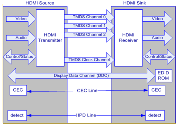
Figure 20-1 Generic HDMI Functional Blocks
Each blocks description are as below:
- HDMI Transmitter/Receiver: High Definition Multimedia Interface Transmitter/Receiver
- TMDS: Transition Minimized Differential Signal
- EDID: Extended Display Identification Data
- CEC: Consumer Electronics Control
- HPD: Hot Plug Detect
A HDMI TX function diagram shows in Figure 20-2.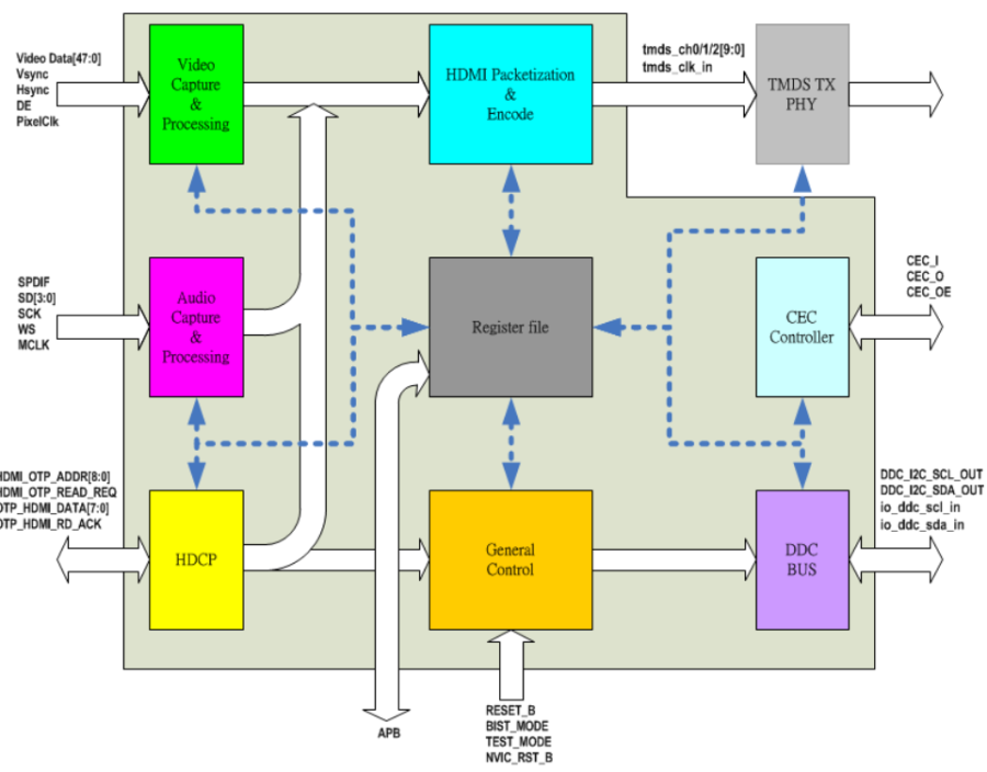
Figure 20-2 HDMI TX Functional Blocks
There are 8 digital sub-blocks in the HDMI TX module of SP7021.
- Video Capture & Processing: Used to capture video data and process video conversion, such as color space conversion.
- Audio Capture & Processing: Used to capture audio data and process audio packetization.
- HDCP: Used to process HDCP authentication between source and sink.
- HDMI packetization: Used to generate TMDS timing protocol and transmit HDMI packets.
- General Control: This block will generate interrupts and resets; the clocks generator also resides here.
- DDC BUS: The hardware DDC (I2C) master to deal with the DDC channel transaction between source and sink.
- CEC: The hardware CEC processor can be a CEC channel transceiver.
- Register File: The register file is to be an interface between host and this module to control HDMI TX.
20.3 Video Path
This HDMI TX module incorporates various video processing modules to perform video conversion such as color space and range as required, and packs into 3 TMDS channels with 8-bits bus each. The detail blocks are drawn as figure 20-3.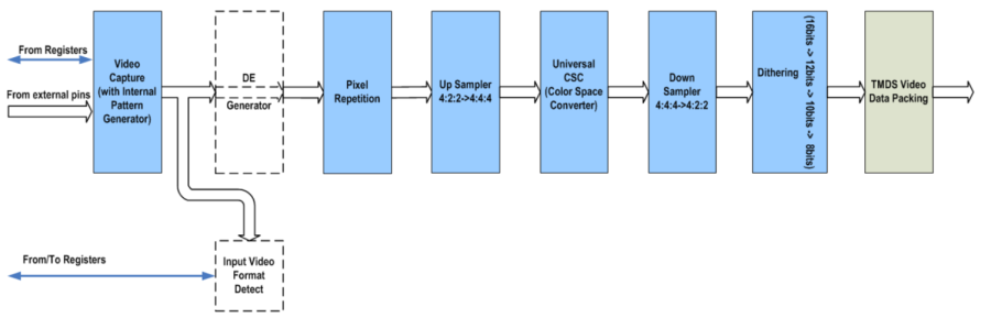
Figure 20-3 Video Path
Three channel YCbCr 4:4:4 <-> two channel YCbCr4:2:2 converters dealing with at most 16-bits video data per channel and a universal color space converter are implemented. For universal CSC composed of one 3x3 matrix, standard ITU-R BT601 and ITU-R BT709 with F(full)/L(limit), F/F, L/F, L/L ranges conversion are supported, and coefficients are configurable according to parameters input as well.
This video processing also has dithering engine to convert 16bits/per channel to 12/10/8bits/per channel. The dithering process is a noise diffusion process for high-intensity-resolution images, which is used to reduce false contouring when the intensity-resolution is decreased.
The video capture receives video data from MPEG side. Because of specific application, this video capture only supports RGB/YCbCr444/YCbCr422 parallel bus input.
For debug purpose, there is an internal video pattern generator in video capture, which provides two patterns, one is gray levels for RGB; the other is color bar for YCbCr.
20.4 Audio Path
This IP supports 2 types of digital audio input channel. One is I2S, the other is SPDIF. I2S can convey L-PCM and HBR (compressed and bit rate > 6.144Mbps, like DTS-HD Master Audio, Dolby MAT), while SPDIF can convey L-PCM and compressed (IEC61937) digital audio.
Digital audio is captured by I2S or SPDIF , then passed them to AUDIO FIFO and packaged into Audio Sample Packet as described in HDMI specification.
Another auxiliary module is ACR module for "Audio Clock Regeneration". This module calculates the "Cycle Time Stamp (CTS)" according to input N value, and packages them into "ACR" packet
. 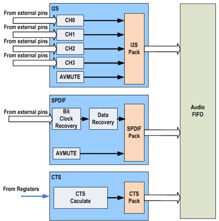
Figure 20-4 Audio Path
20.5 HDCP
Figure 20-5 shows the HDCP function block.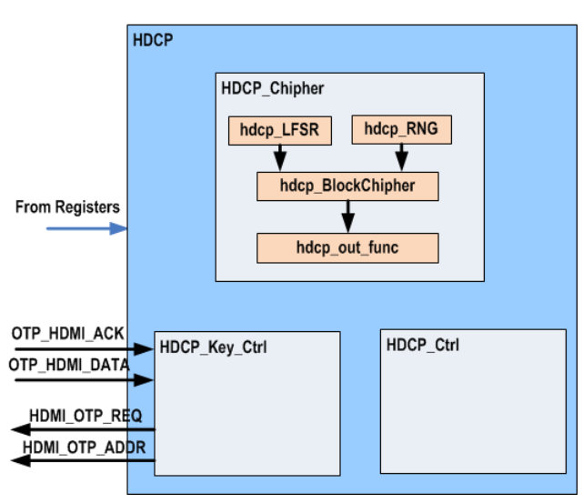
Figure 20-5 HDCP Block
HDMI incorporates HDCP as content protection mechanism during transmitting copyright video and audio data. The SP7021 HDMI TX module embedded a HDCP engine to deal with this task.
The HDCP engine will generate security keys and uses them to encrypt the content. Before transmitting encrypted data, HDMI TX needs to do HDCP authentication with HDMI RX by exchanging HDCP public keys with each other. The detail process can be referred in HDCP specification 1.4.
The HDCP keys should be stored in non-violated memory in a safe place. The SP7021 HDMI TX module incorporates a predefined OTP interface protocol to access HDCP key. By this interface, HDMI TX can get the HDCP key from OTP then does HDCP encryption flow.
20.6 DDC Bus
The DDC bus exchange configuration and status between Source and Sink through I2C. The Sink's configuration and capabilities description is stored in the Extended Display Identification Data (EDID) ROM. The Source shall use I2C commands to read information from a Sink's EDID with a slave address.
20.7 Hot Plug Detect (HPD)
An HDMI Sink shall not assert high voltage level on its Hot Plug Detect pin when the EDID is not available for reading. The Hot Plug Detect pin may be asserted only when the +5V Power line from the Source is detected.
A Source may use a high voltage level Hot Plug Detect signal to initiate the reading of EDID data. A Source shall assume that any voltage within the range specified for High voltage level indicates that a Sink is connected and that EDID is readable.
An HDMI Sink shall indicate any change to the contents of the EDID by driving a low voltage level pulse at (least 100 msec) on the Hot Plug Detect pin.
20.8 Digital Visual Interface (DVI)
SP7021 can also support DVI 1.0 specification. The Group 380.8 SYSTEM CTRL1 register bit0 can select the supported mode. Set bit0=0 for DVI mode, set bit0=1 for HDMI mode.
20.9 System State Control
The firmware will control in the 4 states, they are INIT, HPD, RSEN and HDCP state. The operation flow is shown in figure 20-6. Each state operation describe in table 20-1.
Current State | Next State | Jump Condition |
INIT | INIT | Initialize HW and SW. |
HPD | Go to HPD state after initialization. | |
HPD | HPD | Set AVMUTE, detect HPD, read EDID and parse EDID. |
RSEN | Go to RSEN state when HPD detected and EDID detected or timeout. | |
RSEN | RSEN | Wait HDMI RX stable: enabled, A/V packet configured and TMDS ready. |
HPD | Go back to HPD state when HPD out is detected. | |
HDCP | Go to HDCP state when HDMI TX configuration is finished. | |
HDCP | HDCP | Check HDCP and clear AVMUTE to start to transfer. |
HPD | Go to HPD state when HDP out is detected. | |
RSEN | Go back to RSEN state when HDMI RX out or A/V setting changed. |
Table 20-1 System State Description 
Figure 20-6 HDMI TX main flow state control
20.10 HDMI Interrupts
There are many interrupt events can trigger HDMI TX interrupt. Read Group 383.4 INTR0_STS/383.5 INTR1_STS/383.6 INTR2_STS registers can get the interrupt status. Set corresponding bit to 1 in Group 383.1 INTR0_UNMASK/383.2 INTR1_UNMASK/383.3 INTR2_UNMASK registers can enable the interrupt. Table 20-2 list each interrupt event.
Interrupt status register | Bit | Event |
INTR0_STS | 0 | Hot Plug change detect |
1 | HDMI RX sense change detect | |
2 | Tclk frequency change detect | |
3 | Every Vsync occurs | |
4 | CEC interrupt, refer to "CEC_STS2" | |
9 | CTS value changed detect | |
10 | Audio FIFO empty | |
11 | Audio FIFO full | |
12 | SPDIF preamble error (reserved) | |
113 | SPDIF sample drop (reserved) | |
14 | SPDIF bi-phase error (reserved) | |
15 | SPDIF parity error (reserved) | |
INTR1_STS | 0 | Every 128 HDCP frames |
1 | Every 16 HDCP frames | |
2 | DDC FIFO full | |
3 | DDC FIFO empty | |
4 | Auto Ri check fail @ frame0 | |
5 | Auto Ri check fail @ frame127 | |
6 | TX Ri does not change between frame0 and frame127 | |
7 | Ri/Pj is not read within one frame or DDC bus error | |
8 | Auto Pj check fail @ frame15 | |
9 | TX Pj does not change between frame0 and frame15 | |
INTR2_STS | 0~15 | Reserved |
Table 20-1 HDMI TX Interrupt Event
20.11 Registers Map
20.11.1 Registers Memory Map
Address | Group No. | Register Name | Description |
|---|---|---|---|
0x9C00BE00 | G380.0 | VENDOR ID -- 0x0 | VENDOR ID |
0x9C00BE04 | G380.1 | DEVICE ID -- 0x1 | DEVICE ID |
0x9C00BE08 | G380.2 | Revision -- 0x2 | Revision |
0x9C00BE0C | G380.3 | RESERVED 0003 -- 0x3 | RESERVED 0003 |
0x9C00BE10 | G380.4 | RESERVED 0004 -- 0x4 | RESERVED 0003 |
0x9C00BE14 | G380.5 | PWR CTRL -- 0x5 | PWR CTRL |
0x9C00BE18 | G380.6 | SW RESET -- 0x6 | SW RESET |
0x9C00BE1C | G380.7 | SYSTEM STATUS 0x7 | SYSTEM STATUS |
0x9C00BE20 | G380.8 | SYSTEM CTRL1 -- 0x8 | SYSTEM CTRL1 |
0x9C00BE24 | G380.9 | RESERVED 0009 -- 0x9 | RESERVED 0009 |
0x9C00BE28 | G380.10 | SYSTEM CTRL2 -- 0xa | SYSTEM CTRL2 |
0x9C00BE2C | G380.11 | SYSTEM CTRL3 -- 0xb | SYSTEM CTRL3 |
0x9C00BE30 | G380.12 | SYSTEM CTRL4 -- 0xc | SYSTEM CTRL4 |
0x9C00BE34 | G380.13 | RESERVED 000D -- 0xd | RESERVED 000D |
0x9C00BE38 | G380.14 | RESERVED 000E -- 0xe | RESERVED 000E |
0x9C00BE3C | G380.15 | SYSTEM CTRL5 -- 0xf | SYSTEM CTRL5 |
0x9C00BE40 | G380.16 | HDCP CTRL1 -- 0x10 | HDCP CTRL1 |
0x9C00BE44 | G380.17 | BKSV12 -- 0x11 | BKSV12 |
0x9C00BE48 | G380.18 | BKSV34 -- 0x12 | BKSV34 |
0x9C00BE4C | G380.19 | BKSV5 -- 0x13 | BKSV5 |
0x9C00BE50 | G380.20 | Mi12 -- 0x14 | Mi12 |
0x9C00BE54 | G380.21 | Mi23 -- 0x15 | Mi23 |
0x9C00BE58 | G380.22 | Mi56 -- 0x16 | Mi56 |
0x9C00BE5C | G380.23 | Mi78 -- 0x17 | Mi78 |
0x9C00BE60 | G380.24 | AKSV12 -- 0x18 | AKSV12 |
0x9C00BE64 | G380.25 | AKSV23 -- 0x19 | AKSV23 |
0x9C00BE68 | G380.26 | AKSV5 -- 0x1a | AKSV5 |
0x9C00BE6C | G380.27 | Ri CMP -- 0x1b | Ri CMP |
0x9C00BE70 | G380.28 | Rj CMP -- 0x1c | Rj CMP |
0x9C00BE74 | G380.29 | Ri CMP SET -- 0x1d | Ri CMP SET |
0x9C00BE78 | G380.30 | FrameCnt -- 0x1e | FrameCnt |
0x9C00BE7C | G380.31 | RESERVED 001F -- 0x1f | RESERVED 001F |
Address | Group No. | Register Name | Description |
|---|---|---|---|
0x9C00BE80 | G381.0 | AutoRiCmp -- 0x20 | AutoRiCmp |
0x9C00BE84 | G381.1 | HDCPSTS -- 0x21 | HDCPSTS |
0x9C00BE88 | G381.2 | RXRi -- 0x22 | RXRi |
0x9C00BE8C | G381.3 | RXRj -- 0x23 | RXRj |
0x9C00BE90 | G381.4 | HDCP TEST -- 0x24 | HDCP TEST |
0x9C00BE94 | G381.5 | HDCP TEST RESULT -- 0x25 | HDCP TEST RESULT |
0x9C00BE98 | G381.6 | APO SPDIF CHNL STS0 -- 0x26 | APO SPDIF CHNL STS0 |
0x9C00BE9C | G381.7 | APO SPDIF CHNL STS1 -- 0x27 | APO SPDIF CHNL STS1 |
0x9C00BEA0 | G381.8 | APO SPDIF CHNL STS2 -- 0x28 | APO SPDIF CHNL STS2 |
0x9C00BEA4 | G381.9 | ACR CONFIG2 -- 0x29 | ACR CONFIG2 |
0x9C00BEA8 | G381.10 | ASP URG TH -- 0x2a | ASP URG TH |
0x9C00BEAC | G381.11 | RESERVED 010B -- 0x2b | RESERVED 010B |
0x9C00BEB0 | G381.12 | BLVCTRL -- 0x2c | BLVCTRL |
0x9C00BEB4 | G381.13 | BLVPA0 -- 0x2d | BLVPA0 |
0x9C00BEB8 | G381.14 | BLVPA1 -- 0x2e | BLVPA1 |
0x9C00BEBC | G381.15 | BLVPA2 -- 0x2f | BLVPA2 |
0x9C00BEC0 | G381.16 | VIDEO CTRL1 -- 0x30 | VIDEO CTRL1 |
0x9C00BEC4 | G381.17 | VIDEO IN H STS 0x31 | VIDEO IN H STS |
0x9C00BEC8 | G381.18 | VIDEO IN V STS -- 0x32 | VIDEO IN V STS |
0x9C00BECC | G381.19 | VIDEO DITHER CTRL -- 0x33 | VIDEO DITHER CTRL |
0x9C00BED0 | G381.20 | VIDEO PAT GEN1 -- 0x34 | VIDEO PAT GEN1 |
0x9C00BED4 | G381.21 | VIDEO PAT GEN2 -- 0x35 | VIDEO PAT GEN2 |
0x9C00BED8 | G381.22 | VIDEO PAT GEN3 -- 0x36 | VIDEO PAT GEN3 |
0x9C00BEDC | G381.23 | VIDEO PAT GEN4 -- 0x37 | VIDEO PAT GEN4 |
0x9C00BEE0 | G381.24 | VIDEO PAT GEN5 -- 0x38 | VIDEO PAT GEN5 |
0x9C00BEE4 | G381.25 | VIDEO PAT GEN6 -- 0x39 | VIDEO PAT GEN6 |
0x9C00BEE8 | G381.26 | VIDEO PAT GEN7 -- 0x3a | VIDEO PAT GEN7 |
0x9C00BEEC | G381.27 | VIDEO PAT GEN8 -- 0x3b | VIDEO PAT GEN8 |
0x9C00BEF0 | G381.28 | VIDEO PAT GEN9 -- 0x3c | VIDEO PAT GEN9 |
0x9C00BEF4 | G381.29 | CSC COEFF1 -- 0x3d | CSC COEFF1 |
0x9C00BEF8 | G381.30 | CSC COEFF2 -- 0x3e | CSC COEFF2 |
0x9C00BEFC | G381.31 | CSC COEFF3 -- 0x3f | CSC COEFF3 |
Address | Group No. | Register Name | Description |
|---|---|---|---|
0x9C00BF00 | G382.0 | CSC COEFF4 -- 0x40 | CSC COEFF4 |
0x9C00BF04 | G382.1 | CSC COEFF7 -- 0x41 | CSC COEFF7 |
0x9C00BF08 | G382.2 | CSC COEFF8 -- 0x42 | CSC COEFF8 |
0x9C00BF0C | G382.3 | CSC COEFF9 -- 0x43 | CSC COEFF9 |
0x9C00BF10 | G382.4 | CSC COEFF10 -- 0x44 | CSC COEFF10 |
0x9C00BF14 | G382.5 | CSC COEFF13 -- 0x45 | CSC COEFF13 |
0x9C00BF18 | G382.6 | CSC COEFF14 -- 0x46 | CSC COEFF14 |
0x9C00BF1C | G382.7 | CSC COEFF15 -- 0x47 | CSC COEFF15 |
0x9C00BF20 | G382.8 | CSC COEFF16 -- 0x48 | CSC COEFF16 |
0x9C00BF24 | G382.9 | CSC COEFF19 -- 0x49 | CSC COEFF19 |
0x9C00BF28 | G382.10 | CSC COEFF20 -- 0x4a | CSC COEFF20 |
0x9C00BF2C | G382.11 | CSC COEFF21 -- 0x4b | CSC COEFF21 |
0x9C00BF30 | G382.12 | VIDEO FORMAT -- 0x4c | VIDEO FORMAT |
0x9C00BF34 | G382.13 | RESERVED 020D -- 0x4d | RESERVED 020D |
0x9C00BF38 | G382.14 | AUDIO SW CTS1 -- 0x4e | AUDIO SW CTS1 |
0x9C00BF3C | G382.15 | AUDIO SW CTS2 -- 0x4f | AUDIO SW CTS2 |
0x9C00BF40 | G382.16 | AUDIO CTRL1 -- 0x50 | AUDIO CTRL1 |
0x9C00BF44 | G382.17 | AUDIO CTRL2 -- 0x51 | AUDIO CTRL2 |
0x9C00BF48 | G382.18 | AUDIO SPDIF CTRL -- 0x52 | AUDIO SPDIF CTRL |
0x9C00BF4C | G382.19 | AUDIO SPDIF SW UI -- 0x53 | AUDIO SPDIF SW UI |
0x9C00BF50 | G382.20 | AUDIO SPDIF SW 3UI -- 0x54 | AUDIO SPDIF SW 3UI |
0x9C00BF54 | G382.21 | AUDIO SPDIF HW UI -- 0x55 | AUDIO SPDIF HW UI |
0x9C00BF58 | G382.22 | AUDIO SPDIF HW 3UI -- 0x56 | AUDIO SPDIF HW 3UI |
0x9C00BF5C | G382.23 | AUDIO Chnl STS1 -- 0x57 | AUDIO Chnl STS1 |
0x9C00BF60 | G382.24 | AUDIO Chnl STS2 -- 0x58 | AUDIO Chnl STS2 |
0x9C00BF64 | G382.25 | AUDIO Chnl STS3 -- 0x59 | AUDIO Chnl STS3 |
0x9C00BF68 | G382.26 | ACR CONFIG1 0x5a | ACR CONFIG1 |
0x9C00BF6C | G382.27 | ACR N VALUE1 -- 0x5b | ACR N VALUE1 |
0x9C00BF70 | G382.28 | ACR N VALUE2 -- 0x5c | ACR N VALUE2 |
0x9C00BF74 | G382.29 | ACR HW CTS1 -- 0x5d | ACR HW CTS1 |
0x9C00BF78 | G382.30 | ACR HW CTS2 -- 0x5e | ACR HW CTS2 |
0x9C00BF7C | G382.31 | RESERVED 021F -- 0x5f | RESERVED 021F |
Address | Group No. | Register Name | Description |
|---|---|---|---|
0x9C00BF80 | G383.0 | INTR CTRL -- 0x60 | INTR CTRL |
0x9C00BF84 | G383.1 | INTR0 UNMASK -- 0x61 | INTR0 UNMASK |
0x9C00BF88 | G383.2 | INTR1 UNMASK -- 0x62 | INTR1 UNMASK |
0x9C00BF8C | G383.3 | INTR2 UNMASK -- 0x63 | INTR2 UNMASK |
0x9C00BF90 | G383.4 | INTR0 STS -- 0x64 | INTR0 STS |
0x9C00BF94 | G383.5 | INTR1 STS -- 0x65 | INTR1 STS |
0x9C00BF98 | G383.6 | INTR2 STS -- 0x66 | INTR2 STS |
0x9C00BF9C | G383.7 | DDC MASTER SET 0x67 | DDC MASTER SET |
0x9C00BFA0 | G383.8 | DDC SLV DEVICE ADDR -- 0x68 | DDC SLV DEVICE ADDR |
0x9C00BFA4 | G383.9 | DDC SLV SEG ADDR -- 0x69 | DDC SLV SEG ADDR |
0x9C00BFA8 | G383.10 | DDC SLV REG OFFSET -- 0x6a | DDC SLV REG OFFSET |
0x9C00BFAC | G383.11 | DDC DATA CNT -- 0x6b | DDC DATA CNT |
0x9C00BFB0 | G383.12 | DDC CMD -- 0x6c | DDC CMD |
0x9C00BFB4 | G383.13 | DDC STS 0x6d | DDC STS |
0x9C00BFB8 | G383.14 | DDC DATA -- 0x6e | DDC DATA |
0x9C00BFBC | G383.15 | DDC DATA CNT -- 0x6f | DDC DATA CNT |
0x9C00BFC0 | G383.16 | CEC CONFIG1 -- 0x70 | CEC CONFIG1 |
0x9C00BFC4 | G383.17 | CEC GPIO -- 0x71 | CEC GPIO |
0x9C00BFC8 | G383.18 | CEC DATA SEND -- 0x72 | CEC DATA SEND |
0x9C00BFCC | G383.19 | CEC CONFIG2 -- 0x73 | CEC CONFIG2 |
0x9C00BFD0 | G383.20 | CEC CONFIG3 -- 0x74 | CEC CONFIG3 |
0x9C00BFD4 | G383.21 | CEC CMD -- 0x75 | CEC CMD |
0x9C00BFD8 | G383.22 | CEC TIMER -- 0x76 | CEC TIMER |
0x9C00BFDC | G383.23 | CEC TIMER STS -- 0x77 | CEC TIMER STS |
0x9C00BFE0 | G383.24 | CEC CONFIG4 -- 0x78 | CEC CONFIG4 |
0x9C00BFE4 | G383.25 | CEC DATA RCV -- 0x79 | CEC DATA RCV |
0x9C00BFE8 | G383.26 | CEC STS -- 0x7a | CEC STS |
0x9C00BFEC | G383.27 | CEC STS2 -- 0x7b | CEC STS1 |
0x9C00BFF0 | G383.28 | CEC STS3 -- 0x7c | CEC STS2 |
0x9C00BFF4 | G383.29 | CEC STS4 -- 0x7d | CEC STS3 |
0x9C00BFF8 | G383.30 | RESERVED 031E -- 0x7e | RESERVED 031E |
0x9C00BFFC | G383.31 | RESERVED 031F -- 0x7f | RESERVED 031F |
Address | Group No. | Register Name | Description |
|---|---|---|---|
0x9C00C000 | G384.0 | CEC SEND BYTE12 -- 0x80 | CEC SEND BYTE12 |
0x9C00C004 | G384.1 | CEC SEND BYTE34 -- 0x81 | CEC SEND BYTE34 |
0x9C00C008 | G384.2 | CEC SEND BYTE56 -- 0x82 | CEC SEND BYTE56 |
0x9C00C00C | G384.3 | CEC SEND BYTE78 -- 0x83 | CEC SEND BYTE78 |
0x9C00C010 | G384.4 | CEC SEND BYTE910 -- 0x84 | CEC SEND BYTE910 |
0x9C00C014 | G384.5 | CEC SEND BYTE1112 -- 0x85 | CEC SEND BYTE1112 |
0x9C00C018 | G384.6 | CEC SEND BYTE1314 -- 0x86 | CEC SEND BYTE1314 |
0x9C00C01C | G384.7 | CEC SEND BYTE1516 -- 0x87 | CEC SEND BYTE1516 |
0x9C00C020 | G384.8 | CEC RCV BYTE12 -- 0x88 | CEC RCV BYTE12 |
0x9C00C024 | G384.9 | CEC RCV BYTE34 -- 0x89 | CEC RCV BYTE34 |
0x9C00C028 | G384.10 | CEC RCV BYTE56 -- 0x8a | CEC RCV BYTE56 |
0x9C00C02C | G384.11 | CEC RCV BYTE78 -- 0x8b | CEC RCV BYTE78 |
0x9C00C030 | G384.12 | CEC RCV BYTE910 -- 0x8c | CEC RCV BYTE910 |
0x9C00C034 | G384.13 | CEC RCV BYTE1112 -- 0x8d | CEC RCV BYTE1112 |
0x9C00C038 | G384.14 | CEC RCV BYTE1314 -- 0x8e | CEC RCV BYTE1314 |
0x9C00C03C | G384.15 | CEC RCV BYTE1516 -- 0x8f | CEC RCV BYTE1516 |
0x9C00C040 | G384.16 | Universal InFoFrame HB01 -- 0x90 | Universal InFoFrame HB01 |
0x9C00C044 | G384.17 | Universal InFoFrame HB02 -- 0x91 | Universal InFoFrame HB02 |
0x9C00C048 | G384.18 | Universal PacketBody01 -- 0x92 | Universal PacketBody01 |
0x9C00C04C | G384.19 | Universal PacketBody23 -- 0x93 | Universal PacketBody23 |
0x9C00C050 | G384.20 | Universal PacketBody45 -- 0x94 | Universal PacketBody45 |
0x9C00C054 | G384.21 | Universal PacketBody67 -- 0x95 | Universal PacketBody67 |
0x9C00C058 | G384.22 | Universal PacketBody89 -- 0x96 | Universal PacketBody89 |
0x9C00C05C | G384.23 | Universal PacketBody1011 -- 0x97 | Universal PacketBody1011 |
0x9C00C060 | G384.24 | Universal PacketBody1213 -- 0x98 | Universal PacketBody1213 |
0x9C00C064 | G384.25 | Universal PacketBody1415 -- 0x98 | Universal PacketBody1415 |
0x9C00C068 | G384.26 | Universal PacketBody1617 -- 0x9a | Universal PacketBody1617 |
0x9C00C06C | G384.27 | Universal PacketBody1819 -- 0x9b | Universal PacketBody1819 |
0x9C00C070 | G384.28 | Universal PacketBody2021 -- 0x9c | Universal PacketBody2021 |
0x9C00C074 | G384.29 | Universal PacketBody2223 -- 0x9d | Universal PacketBody2223 |
0x9C00C078 | G384.30 | Universal PacketBody2425 -- 0x9e | Universal PacketBody2425 |
0x9C00C07C | G384.31 | Universal PacketBody2627 -- 0x9f | Universal PacketBody2627 |
Address | Group No. | Register Name | Description |
|---|---|---|---|
0x9C00C080 | G385.0 | InfoFrame CTRL1 0xa0 | InfoFrame CTRL1 |
0x9C00C084 | G385.1 | InfoFrame CTRL2 0xa1 | InfoFrame CTRL2 |
0x9C00C088 | G385.2 | InfoFrame CTRL3 0xa2 | InfoFrame CTRL3 |
0x9C00C08C | G385.3 | InfoFrame CTRL4 0xa3 | InfoFrame CTRL4 |
0x9C00C090 | G385.4 | InfoFrame CTRL5 0xa4 | InfoFrame CTRL5 |
0x9C00C094 | G385.5 | InfoFrame CTRL6 0xa5 | InfoFrame CTRL6 |
0x9C00C098 | G385.6 | AVI InfoFrame01 -- 0xa6 | AVI InfoFrame01 |
0x9C00C09C | G385.7 | AVI InfoFrame23 -- 0xa7 | AVI InfoFrame23 |
0x9C00C0A0 | G385.8 | AVI InfoFrame45 -- 0xa8 | AVI InfoFrame45 |
0x9C00C0A4 | G385.9 | AVI InfoFrame67 -- 0xa9 | AVI InfoFrame67 |
0x9C00C0A8 | G385.10 | AVI InfoFrame89 -- 0xaa | AVI InfoFrame89 |
0x9C00C0AC | G385.11 | AVI InfoFrame1011 -- 0xab | AVI InfoFrame1011 |
0x9C00C0B0 | G385.12 | AVI InfoFrame1213 -- 0xac | AVI InfoFrame1213 |
0x9C00C0B4 | G385.13 | AUDIO InfoFrame01 -- 0xad | AUDIO InfoFrame01 |
0x9C00C0B8 | G385.14 | AUDIO InfoFrame23 -- 0xae | AUDIO InfoFrame23 |
0x9C00C0BC | G385.15 | AUDIO InfoFrame45 -- 0xaf | AUDIO InfoFrame45 |
0x9C00C0C0 | G385.16 | AUDIO InfoFrame67 -- 0xb0 | AUDIO InfoFrame67 |
0x9C00C0C4 | G385.17 | AUDIO InfoFrame89 -- 0xb1 | AUDIO InfoFrame89 |
0x9C00C0C8 | G385.18 | AUDIO InfoFrame1011 -- 0xb2 | AUDIO InfoFrame1011 |
0x9C00C0CC | G385.19 | General Control Packet -- 0xb3 | General Control Packet |
0x9C00C0D0 | G385.20 | ACP Packet Header -- 0xb4 | ACP Packet Header |
0x9C00C0D4 | G385.21 | ACP Packet Body01 -- 0xb5 | ACP Packet Body01 |
0x9C00C0D8 | G385.22 | ACP Packet Body23 -- 0xb6 | ACP Packet Body23 |
0x9C00C0DC | G385.23 | ACP Packet Body45 -- 0xb7 | ACP Packet Body45 |
0x9C00C0E0 | G385.24 | ACP Packet Body67 -- 0xb8 | ACP Packet Body67 |
0x9C00C0E4 | G385.25 | ACP Packet Body89 -- 0xb9 | ACP Packet Body89 |
0x9C00C0E8 | G385.26 | ACP Packet Body1011 -- 0xba | ACP Packet Body1011 |
0x9C00C0EC | G385.27 | ACP Packet Body1213 -- 0xbb | ACP Packet Body1213 |
0x9C00C0F0 | G385.28 | ACP Packet Body1415 -- 0xbc | ACP Packet Body1415 |
0x9C00C0F4 | G385.29 | ACP Packet Body1617 -- 0xbd | ACP Packet Body1617 |
0x9C00C0F8 | G385.30 | ACP Packet Body1819 -- 0xbe | ACP Packet Body1819 |
0x9C00C0FC | G385.31 | ACP Packet Body2021 -- 0xbf | ACP Packet Body2021 |
Address | Group No. | Register Name | Description |
|---|---|---|---|
0x9C00C100 | G386.0 | ACP Packet Body2223 -- 0xc0 | ACP Packet Body2223 |
0x9C00C104 | G386.1 | ACP Packet Body2425 -- 0xc1 | ACP Packet Body2425 |
0x9C00C108 | G386.2 | ACP Packet Body2627 -- 0xc2 | ACP Packet Body2627 |
0x9C00C10C | G386.3 | Vendor Specific InfoFrame -- 0xc3 | Vendor Specific InfoFrame |
0x9C00C110 | G386.4 | Vendor Specific Length -- 0xc4 | Vendor Specific Length |
0x9C00C114 | G386.5 | SPD InfoFrame PB01 -- 0xc5 | SPD InfoFrame PB01 |
0x9C00C118 | G386.6 | SPD InfoFrame PB23 -- 0xc6 | SPD InfoFrame PB23 |
0x9C00C11C | G386.7 | SPD InfoFrame PB45 -- 0xc7 | SPD InfoFrame PB45 |
0x9C00C120 | G386.8 | SPD InfoFrame PB67 -- 0xc8 | SPD InfoFrame PB67 |
0x9C00C124 | G386.9 | SPD InfoFrame PB89 -- 0xc9 | SPD InfoFrame PB89 |
0x9C00C128 | G386.10 | SPD InfoFrame PB1011 -- 0xc10 | SPD InfoFrame PB1011 |
0x9C00C12C | G386.11 | SPD InfoFrame PB1213 -- 0xc11 | SPD InfoFrame PB1213 |
0x9C00C130 | G386.12 | SPD InfoFrame PB1415 -- 0xc12 | SPD InfoFrame PB1415 |
0x9C00C134 | G386.13 | SPD InfoFrame PB1617 -- 0xc13 | SPD InfoFrame PB1617 |
0x9C00C138 | G386.14 | SPD InfoFrame PB1819 -- 0xc14 | SPD InfoFrame PB1819 |
0x9C00C13C | G386.15 | SPD InfoFrame PB2021 -- 0xc15 | SPD InfoFrame PB2021 |
0x9C00C140 | G386.16 | SPD InfoFrame PB2223-- 0xc16 | SPD InfoFrame PB2223 |
0x9C00C144 | G386.17 | SPD InfoFrame PB2425 -- 0xc17 | SPD InfoFrame PB2425 |
0x9C00C148 | G386.18 | ISRC packet header -- 0xd2 | ISRC packet header |
0x9C00C14C | G386.19 | ISRC1 PB01 -- 0xd3 | ISRC1 PB01 |
0x9C00C150 | G386.20 | ISRC1 PB23 -- 0xd4 | ISRC1 PB23 |
0x9C00C154 | G386.21 | ISRC1 PB45 -- 0xd5 | ISRC1 PB45 |
0x9C00C158 | G386.22 | ISRC1 PB67 -- 0xd6 | ISRC1 PB67 |
0x9C00C15C | G386.23 | ISRC1 PB89 -- 0xd7 | ISRC1 PB89 |
0x9C00C160 | G386.24 | ISRC1 PB1011 -- 0xd8 | ISRC1 PB1011 |
0x9C00C164 | G386.25 | ISRC1 PB1213 -- 0xd9 | ISRC1 PB1213 |
0x9C00C168 | G386.26 | ISRC1 PB1415 -- 0xda | ISRC1 PB1415 |
0x9C00C16C | G386.27 | ISRC2 PB01 -- 0xdb | ISRC2 PB01 |
0x9C00C170 | G386.28 | ISRC2 PB23 -- 0xdc | ISRC2 PB23 |
0x9C00C174 | G386.29 | ISRC2 PB45 -- 0xdd | ISRC2 PB45 |
0x9C00C178 | G386.30 | ISRC2 PB67 -- 0xde | ISRC2 PB67 |
0x9C00C17C | G386.31 | ISRC2 PB89 -- 0xdf | ISRC2 PB89 |
Address | Group No. | Register Name | Description |
|---|---|---|---|
0x9C00C180 | G387.0 | ISRC2 PB1011 -- 0xe0 | ISRC2 PB1011 |
0x9C00C184 | G387.1 | ISRC2 PB1213 -- 0xe1 | ISRC2 PB1213 |
0x9C00C188 | G387.2 | ISRC2 PB1415 -- 0xe2 | ISRC2 PB1415 |
0x9C00C18C | G387.3 | Gamut Metadata Packet Header --0xe3 | Gamut Metadata Packet Header |
0x9C00C190 | G387.4 | Gamut Metatata Packet PB01 --0xe4 | Gamut Metatata Packet PB01 |
0x9C00C194 | G387.5 | Gamut Metatata Packet PB23 --0xe5 | Gamut Metatata Packet PB23 |
0x9C00C198 | G387.6 | Gamut Metatata Packet PB45 --0xe6 | Gamut Metatata Packet PB45 |
0x9C00C19C | G387.7 | Gamut Metatata Packet PB67 --0xe7 | Gamut Metatata Packet PB67 |
0x9C00C1A0 | G387.8 | Gamut Metatata Packet PB89 --0xe8 | Gamut Metatata Packet PB89 |
0x9C00C1A4 | G387.9 | Gamut Metatata Packet PB1011 --0xe9 | Gamut Metatata Packet PB1011 |
0x9C00C1A8 | G387.10 | Gamut Metatata Packet PB1213 --0xea | Gamut Metatata Packet PB1213 |
0x9C00C1AC | G387.11 | Gamut Metatata Packet PB1415 --0xeb | Gamut Metatata Packet PB1415 |
0x9C00C1B0 | G387.12 | Gamut Metatata Packet PB1617 --0xec | Gamut Metatata Packet PB1617 |
0x9C00C1B4 | G387.13 | Gamut Metatata Packet PB1819 --0xed | Gamut Metatata Packet PB1819 |
0x9C00C1B8 | G387.14 | Gamut Metatata Packet PB2021 --0xee | Gamut Metatata Packet PB2021 |
0x9C00C1BC | G387.15 | Gamut Metatata Packet PB2223 --0xef | Gamut Metatata Packet PB2223 |
0x9C00C1C0 | G387.16 | Gamut Metatata Packet PB2425 --0xf0 | Gamut Metatata Packet PB2425 |
0x9C00C1C4 | G387.17 | Gamut Metatata Packet PB2627 --0xf1 | Gamut Metatata Packet PB2627 |
0x9C00C1C8 | G387.18 | MPEG Source InfoFrame PB01 --0xf2 | MPEG Source InfoFrame PB01 |
0x9C00C1CC | G387.19 | MPEG Source InfoFrame PB23 --0xf3 | MPEG Source InfoFrame PB23 |
0x9C00C1D0 | G387.20 | MPEG Source InfoFrame PB45 --0xf4 | MPEG Source InfoFrame PB45 |
0x9C00C1D4 | G387.21 | MPEG Source InfoFrame PB67 --0xf5 | MPEG Source InfoFrame PB67 |
0x9C00C1D8 | G387.22 | MPEG Source InfoFrame PB89 --0xf6 | MPEG Source InfoFrame PB89 |
0x9C00C1DC | G387.23 | MPEG Source InfoFrame PB10 --0xf7 | MPEG Source InfoFrame PB10 |
0x9C00C1E0 | G387.24 | RESERVED 0718 -- 0xf8 | RESERVED 0718 |
0x9C00C1E4 | G387.25 | RESERVED 0719 -- 0xf9 | RESERVED 0719 |
0x9C00C1E8 | G387.26 | TMDSTX CTRL1 -- 0xfa | TMDSTX CTRL1 |
0x9C00C1EC | G387.27 | TMDSTX CTRL2 -- 0xfb | TMDSTX CTRL2 |
0x9C00C1F0 | G387.28 | TMDSTX CTRL3 -- 0xfc | TMDSTX CTRL3 |
0x9C00C1F4 | G387.29 | TMDSTX CTRL4 -- 0xfd | TMDSTX CTRL4 |
0x9C00C1F8 | G387.30 | TMDSTX CTRL5 -- 0xfe | TMDSTX CTRL5 |
0x9C00C1FC | G387.31 | RESERVED 071F -- 0xff | RESERVED 071F |
20.11.2 Registers Description
RGST Table Group 380 HDMI G0
380.0 VENDOR ID ( VENDOR ID -- 0x0 )
Address: 0x9C00BE00
Reset: 0x2401
| Field Name | Bit | Access | Description |
| VENDOR ID | 15:0 | RO | Vendor ID Sunplus ID (0x2401) |
380.1 DEVICE ID ( DEVICE ID -- 0x1 )
Address: 0x9C00BE04
Reset: 0x1329
| Field Name | Bit | Access | Description |
| DEVICE | 15:0 | RO | Device ID CARBON ID (0x1329) |
380.2 Revision ( Revision -- 0x2 )
Address: 0x9C00BE08
Reset: 0x2000
| Field Name | Bit | Access | Description |
| Revision | 15:0 | RO | IP Revision |
380.3 RESERVED 0003 ( RESERVED 0003 -- 0x3 )
Address: 0x9C00BE0C
Reset: 0x0000
| Field Name | Bit | Access | Description |
| Reserved | 15:0 | RW | Reserved |
380.4 RESERVED 0004 ( RESERVED 0004 -- 0x4 )
Address: 0x9C00BE10
Reset: 0x0000
| Field Name | Bit | Access | Description |
| Reserved | 15:0 | RW | Reserved |
380.5 PWR CTRL ( PWR CTRL -- 0x5 )
Address: 0x9C00BE14
Reset: 0x140f
| Field Name | Bit | Access | Description |
| Reserved | 15:14 | RW | Reserved |
| aclk sel | 13:12 | RW | Audio clock freq. select (ACLK from TMDSTX) Faclk = 4*Ftclk/N. |
| oclk src sel | 11:10 | RW | Audio Sample Clock Source select (mainly for SPDIF sampling) |
| tclk edge | 9 | RW | Adjust tclk edge, 0: Non-inverted 1: Inverted |
| pclk edge | 8 | RW | Adjust pclk edge, 0: Non-inverted 1: Inverted |
| Reserved | 7:5 | RW | Reserved |
| pd tmds n | 4 | RW | Power down TMDSTX PHY, 0: pwr down, 1: normal |
| pd tclk | 3 | RW | Power down tclk domain, 0: pwr down 1: normal |
| pd fclk n | 2 | RW | Power down fclk domain, 0: pwr down 1: normal |
| pd pclk n | 1 | RW | Power down pclk domain, 0: pwr down 1: normal |
| pd total n | 0 | RW | Power down all, 0: pwr down, 1: normal |
380.6 SW RESET ( SW RESET -- 0x6 )
Address: 0x9C00BE18
Reset: 0x00e9
| Field Name | Bit | Access | Description |
| Reserved | 15:8 | RW | Reserved |
| TMDS_rst_b | 7 | RW | TMDS reset 0: reset, 1: normal |
| Audio_rst_b | 6 | RW | Audio reset 0: reset, 1: normal |
| Video_rst_b | 5 | RW | Video reset 0: reset, 1: normal |
| RW afifo_lp_en | 4 | RW | Audio FIFO Low Power Enable 0: disable, 1: enable |
| CEC_rst_b | 3 | RW | CEC reset 0: reset, 1: normal |
| HDCP_rst_b | 2 | RW | HDCP Engine reset 0: reset, 1: normal |
| FIFO_rst_b | 1 | RW | Audio FIFO reset 0: reset, 1: normal |
| SW_ rst_b | 0 | RW | Software reset 0: reset, 1: normal |
380.7 SYSTEM STATUS ( SYSTEM STATUS 0x7 )
Address: 0x9C00BE1C
Reset: 0x0000
| Field Name | Bit | Access | Description |
| Reserved | 15:4 | RW | Reserved |
| tmds clkdetect | 3 | RU | TMDS clock detect. (Clock sources from TMDS PHY) 0: No TMDS clock. 1: TMDS clock exist |
| pll_ready | 2 | RU | Internal PLL ready. (for reference only) 0: Not ready. 1: Ready |
| hpd_in | 1 | RU | Hot Plug Detect status 0: No Hot Plug. 1: Hot Plug In (Usually means HDMI RX is connected) |
| rsen in | 0 | RU | HDMI RX sense 0: No Rx. 1: Rx active (HDMI RX is powered) |
380.8 SYSTEM CTRL1 ( SYSTEM CTRL1 -- 0x8 )
Address: 0x9C00BE20
Reset: 0x1000
| Field Name | Bit | Access | Description |
| Reserved | 15:12 | RW | Reserved |
| Reserved | 11:3 | RW | Reserved |
| null packet en | 2 | RW | Auto null packet enable 0: Disable NULL packet 1: Enable NULL packet |
| Reserved | 1 | RW | Reserved |
| hdmi mode | 0 | RW | HDMI mode or DVI mode. 0: DVI mode. 1: HDMI mode |
380.9 RESERVED 0009 ( RESERVED 0009 -- 0x9 )
Address: 0x9C00BE24
Reset: 0x0000
| Field Name | Bit | Access | Description |
| Reserved | 15:0 | RW | Reserved |
380.10 SYSTEM CTRL2 ( SYSTEM CTRL2 -- 0xa )
Address: 0x9C00BE28
Reset: 0x0000
| Field Name | Bit | Access | Description |
| Reserved | 15:3 | RW | Reserved |
| Reserved | 2 | RW | Reserved |
| Reserved | 1 | RW | Reserved |
| Reserved | 0 | RW | Reserved |
380.11 SYSTEM CTRL3 ( SYSTEM CTRL3 -- 0xb )
Address: 0x9C00BE2C
Reset: 0x0697
| Field Name | Bit | Access | Description |
| hpd deb delay | 15:0 | RW | Hot Plug Detection debounce counter If HPD signal is unstable, try to increase this value |
380.12 SYSTEM CTRL4 ( SYSTEM CTRL4 -- 0xc )
Address: 0x9C00BE30
Reset: 0x0010
| Field Name | Bit | Access | Description |
| ddc deb delay | 15:0 | RW | DDC signal debounce counter If DDC signal is unstable, try to increase this value |
380.13 RESERVED 000D ( RESERVED 000D -- 0xd )
Address: 0x9C00BE34
Reset: 0x0000
| Field Name | Bit | Access | Description |
| Reserved | 15:0 | RW | Reserved |
380.14 RESERVED 000E ( RESERVED 000E -- 0xe )
Address: 0x9C00BE38
Reset: 0x0000
| Field Name | Bit | Access | Description |
| Reserved | 15:0 | RW | Reserved |
380.15 SYSTEM CTRL5 ( SYSTEM CTRL5 -- 0xf )
Address: 0x9C00BE3C
Reset: 0x8000
| Field Name | Bit | Access | Description |
| Reserved | 15:0 | RW | Reserved |
380.16 HDCP CTRL1 ( HDCP CTRL1 -- 0x10 )
Address: 0x9C00BE40
Reset: 0x0008
| Field Name | Bit | Access | Description |
| Reserved | 15:0 | RW | Reserved |
380.17 BKSV12 ( BKSV12 -- 0x11 )
Address: 0x9C00BE44
Reset: 0x0000
| Field Name | Bit | Access | Description |
| Reserved | 15:0 | RW | Reserved |
380.18 BKSV34 ( BKSV34 -- 0x12 )
Address: 0x9C00BE48
Reset: 0x0000
| Field Name | Bit | Access | Description |
| Reserved | 15:0 | RW | Reserved |
380.19 BKSV5 ( BKSV5 -- 0x13 )
Address: 0x9C00BE4C
Reset: 0x0000
| Field Name | Bit | Access | Description |
| Reserved | 15:0 | RW | Reserved |
380.20 Mi12 ( Mi12 -- 0x14 )
Address: 0x9C00BE50
Reset: 0x0000
| Field Name | Bit | Access | Description |
| Reserved | 15:0 | RW | Reserved |
380.21 Mi23 ( Mi23 -- 0x15 )
Address: 0x9C00BE54
Reset: 0x0000
| Field Name | Bit | Access | Description |
| Reserved | 15:0 | RW | Reserved |
380.22 Mi56 ( Mi56 -- 0x16 )
Address: 0x9C00BE58
Reset: 0x0000
| Field Name | Bit | Access | Description |
| Reserved | 15:0 | RW | Reserved |
380.23 Mi78 ( Mi78 -- 0x17 )
Address: 0x9C00BE5C
Reset: 0x0000
| Field Name | Bit | Access | Description |
| Reserved | 15:0 | RW | Reserved |
380.24 AKSV12 ( AKSV12 -- 0x18 )
Address: 0x9C00BE60
Reset: 0x0000
| Field Name | Bit | Access | Description |
| Reserved | 15:0 | RW | Reserved |
380.25 AKSV23 ( AKSV23 -- 0x19 )
Address: 0x9C00BE64
Reset: 0x0000
| Field Name | Bit | Access | Description |
| Reserved | 15:0 | RW | Reserved |
380.26 AKSV5 ( AKSV5 -- 0x1a )
Address: 0x9C00BE68
Reset: 0x0000
| Field Name | Bit | Access | Description |
| Reserved | 15:0 | RW | Reserved |
380.27 Ri CMP ( Ri CMP -- 0x1b )
Address: 0x9C00BE6C
Reset: 0x0000
| Field Name | Bit | Access | Description |
| Reserved | 15:0 | RW | Reserved |
380.28 Rj CMP ( Rj CMP -- 0x1c )
Address: 0x9C00BE70
Reset: 0x0000
| Field Name | Bit | Access | Description |
| Reserved | 15:0 | RW | Reserved |
380.29 Ri CMP SET ( Ri CMP SET -- 0x1d )
Address: 0x9C00BE74
Reset: 0x0000
| Field Name | Bit | Access | Description |
| Reserved | 15:0 | RW | Reserved |
380.30 FrameCnt ( FrameCnt -- 0x1e )
Address: 0x9C00BE78
Reset: 0x0000
| Field Name | Bit | Access | Description |
| Reserved | 15:7 | RW | Reserved |
| HDt frame count | 6:0 | RO | Current HDCP frame count. The HDCP frame count is from 0 to 127. |
380.31 RESERVED 001F ( RESERVED 001F -- 0x1f )
Address: 0x9C00BE7C
Reset: 0x0000
| Field Name | Bit | Access | Description |
| Reserved | 15:0 | RW | Reserved |
RGST Table Group 381 HDMI G1
381.0 AutoRiCmp ( AutoRiCmp -- 0x20 )
Address: 0x9C00BE80
Reset: 0x0000
| Field Name | Bit | Access | Description |
| Reserved | 15:1 | RW | Reserved |
| Auto RI En | 0 | RW | 1 = Enable hardware Auto-Ri check 0 = Use SW to do Ri check |
381.1 HDCPSTS ( HDCPSTS -- 0x21 )
Address: 0x9C00BE84
Reset: 0x0000
| Field Name | Bit | Access | Description |
| Reserved | 15:6 | RW | Reserved |
| DBf RI check bus error | 5 | RO | 1 = DDC Bus fail when doing Auto-Ri compare |
| DBf TXPJ no change | 4 | RO | 1 = Pj is not changed @ HDMI transmitter |
| DBf PJ check fail | 3 | RO | 1 = Auto-Pj comapre fail |
| DBf TXRI no change | 2 | RO | 1 = Ri is not changed @ HDMI transmitter |
| DBf RI Frame127 check fail | 1 | RO | 1 = Auto-Ri comapre fail @ HDCP frame == 127 |
| DBf RI Frame0 check fail | 0 | RO | 1= Auto-Ri comaprefail @HDCP frame == RI Comp Frame |
381.2 RXRi ( RXRi -- 0x22 )
Address: 0x9C00BE88
Reset: 0x0000
| Field Name | Bit | Access | Description |
| Reserved | 15:0 | RW | Reserved |
381.3 RXPj ( RXPj -- 0x23 )
Address: 0x9C00BE8C
Reset: 0x0000
| Field Name | Bit | Access | Description |
| Reserved | 15:0 | RW | Reserved |
381.4 HDCP TEST ( HDCP TEST -- 0x24 )
Address: 0x9C00BE90
Reset: 0x0000
| Field Name | Bit | Access | Description |
| Reserved | 15:0 | RW | Reserved |
381.5 HDCP TEST RESULT ( HDCP TEST RESULT -- 0x25 )
Address: 0x9C00BE94
Reset: 0x0000
| Field Name | Bit | Access | Description |
| Reserved | 15:4 | RW | Reserved |
| HDf HDCP Bist2 err | 3 | RO | HDMI Self-Test#2 Fail flag 0: HDMI Self-Test#2 Pass |
| HDf HDCP Bist2 done | 2 | RO | HDMI Self-Test#2 Done flag 0: HDMI Self-Test#2 not Done 1: HDMI Self-Test#2 Done |
| HDf HDCP Bist1 err | 1 | RO | HDMI Self-Test#1 Fail flag 0: HDMI Self-Test#1 Pass |
| HDf HDCP Bist1 done | 0 | RO | HDMI Self-Test#1 Done flag 0: HDMI Self-Test#1 not Done 1: HDMI Self-Test#1 DoneWhen this bit is 1, then check the following result. |
381.6 APO SPDIF CHNL STS0 ( APO SPDIF CHNL STS0 -- 0x26 )
Address: 0x9C00BE98
Reset: 0x0000
| Field Name | Bit | Access | Description |
| APo spdif chnl sts[15:0] | 15:0 | RO | Channel status[15:0] of SPDIF |
381.7 APO SPDIF CHNL STS1 ( APO SPDIF CHNL STS1 -- 0x27 )
Address: 0x9C00BE9C
Reset: 0x0000
| Field Name | Bit | Access | Description |
| APo spdif chnl sts[31:16] | 15:0 | RO | Channel status[31:16] of SPDIF |
381.8 APO SPDIF CHNL STS2 ( APO SPDIF CHNL STS2 -- 0x28 )
Address: 0x9C00BEA0
Reset: 0x0000
| Field Name | Bit | Access | Description |
| APo spdif chnl sts[47:32] | 15:0 | RO | Channel status[47:32] of SPDIF |
381.9 ACR CONFIG2 ( ACR CONFIG2 -- 0x29 )
Address: 0x9C00BEA4
Reset: 0x0002
| Field Name | Bit | Access | Description |
| Reserved | 15:3 | RW | Reserved |
| asp urgent en | 2 | RW | Audio Sample Packet Urgent Enable (left it default) 0: Disable ASP urgent 1: Enable ASP urgent |
| bw ctrl en | 1 | RW | Audio bandwidth control register. 0: Disable 1: Enable |
| spdif adaptive ui en | 0 | RW | Adaptive ui control register. 0: Disable 1: Enable |
381.10 ASP URG TH ( ASP URG TH -- 0x2a )
Address: 0x9C00BEA8
Reset: 0x0000
| Field Name | Bit | Access | Description |
| asp urgent thr high | 15:8 | RW | ASP urgent threshold setting, upper bound |
| asp urgent thr low | 7:0 | RW | ASP urgent threshold setting, lower bound |
381.11 RESERVED 010B ( RESERVED 010B -- 0x2b )
Address: 0x9C00BEAC
Reset: 0x0000
| Field Name | Bit | Access | Description |
| Reserved | 15:0 | RW | Reserved |
381.12 BLVCTRL ( BLVCTRL -- 0x2c )
Address: 0x9C00BEB0
Reset: 0x0000
| Field Name | Bit | Access | Description |
| Reserved | 15:3 | RW | Reserved |
| csc man dst c | 2 | RW | CSC man mode for RL2RF/RF2RL/YL2YF/YF2YL 0: keep hw definition of destination side color space 1: change hw definition of destination side color space |
| csc man src c | 1 | RW | CSC man mode for RL2RF/RF2RL/YL2YF/YF2YL 0: keep hw definition of source side color space 1: change hw definition of source side color space |
| blvipa en | 0 | RW | Internal blank video switch 0: Disable 1: Enable |
381.13 BLVPA0 ( BLVPA0 -- 0x2d )
Address: 0x9C00BEB4
Reset: 0x0000
| Field Name | Bit | Access | Description |
| blvipa ch0 | 15:0 | RW | Internal blank video ch0 (B/Cb) |
381.14 BLVPA1 ( BLVPA1 -- 0x2e )
Address: 0x9C00BEB8
Reset: 0x0000
| Field Name | Bit | Access | Description |
| blvipa ch1 | 15:0 | RW | Internal blank video ch1 (G/Y) |
381.15 BLVPA2 ( BLVPA2 -- 0x2f )
Address: 0x9C00BEBC
Reset: 0x0000
| Field Name | Bit | Access | Description |
| blvipa ch2 | 15:0 | RW | Internal blank video ch2 (R/Cr) |
381.16 VIDEO CTRL1 ( VIDEO CTRL1 -- 0x30 )
Address: 0x9C00BEC0
Reset: 0x0000
| Field Name | Bit | Access | Description |
| vs_pol_reg | 15 | RW | vsync polarity 0: negative sync 1: positive sync |
| hs_pol_reg | 14 | RW | hsync polarity 0: negative sync 1: positive syncc |
| sync_pol_set | 13 | RW | video sync polarity settings: 0: auto 1: controlled by registers (0x10[15:14]) |
| downsample | 12 | RW | down-sample enable 1: 444 to 422 enable (down-sample) Only valid in YC mode. |
| upsample | 11 | RW | up-sample enable 1: 422 to 444 enable (up-sample) Only valid in YC mode. |
| Reserved | 10 | RW | Reserved |
| csc_man | 9 | RW | color space coversion coefficient control 0: color space coversion coefficient is predefined. |
| csc_en | 8 | RW | color space coversion enable 0: color space coversion disable 1: color space coversion enable |
| csc_mode | 7:4 | RW | color space conversion mode: bit [0] 0=limit range ycc, 1=full range ycc bit [1] 0=limit range rgb, 1=full range rgb bit [2] 0=r2y, 1=y2r bit [3] 0=601 (SSD), 1=709 (HD) |
| pix rep | 3:0 | RW | pixel repitition: 0 = no repeat 1 = sent 2 times 2 = sent 3 times 3 = sent 4 times 4 = sent 5 times 5 = sent 6 times 6 = sent 7 times 7 = sent 8 times 8 = sent 9 times 9 = sent 10 times |
381.17 VIDEO IN H STS ( VIDEO IN H STS 0x31 )
Address: 0x9C00BEC4
Reset: 0x8000
| Field Name | Bit | Access | Description |
| VPp hs pol | 15 | RU | hardware detected hync polarity |
| Reserved | 14:13 | RW | Reserved |
| VPp hres | 12:0 | RU | hardware detected hync resolution |
381.18 VIDEO IN V STS ( VIDEO IN V STS -- 0x32 )
Address: 0x9C00BEC8
Reset: 0x8000
| Field Name | Bit | Access | Description |
| VPp vs pol | 15 | RO | hardware detected vync polarity |
| Reserved | 14:12 | RW | Reserved |
| VPp vres | 11:0 | RO | hardware detected vync resolution |
381.19 VIDEO DITHER CTRL ( VIDEO DITHER CTRL -- 0x33 )
Address: 0x9C00BECC
Reset: 0x0000
| Field Name | Bit | Access | Description |
| Reserved | 15:5 | RW | Reserved |
| tdither en | 4 | RW | enable time domain dithering 0: disable time domain dithering 1: enable time domain dithering |
| dither mode | 3:1 | RW | dithering mode 0x0: dither off 0x1: dither on, 16bits to 12bits 0x2: dither on, 16bits to 10bits 0x3: dither on, 16bits to 8bits 0x4: dither on, 12bits to 10bits 0x5: dither on, 12bits to 8bits 0x6: dither on, 10bits to 8bits |
| dither en | 0 | RW | dithering enable 0: dithering disable 1: dithering enable |
381.20 VIDEO PAT GEN1 ( VIDEO PAT GEN1 -- 0x34 )
Address: 0x9C00BED0
Reset: 0x0000
| Field Name | Bit | Access | Description |
| Reserved | 15:13 | RW | Reserved |
| vg inter mode | 12:11 | RW | interlaced internal pattern resolution selection: 0: disable 1: 480i 2: 576i 3: 1080i |
| pat res | 10:8 | RW | internal pattern resolution selection: 0: 480p 1: 720p 2: 1080p 3: 4k x 2k @ 24Hz 7: registers define (reg: 0x15 0x1C) (other setting are un-defined) |
| gray step | 7:6 | RW | gray level steps: 0: 1 step 1: 4 steps 2: 16 steps 3: 64 steps |
| yc_HD_SD | 5 | RW | ycc color bar pattern with HD or SD: 0: SD (601) 1: HD (709) |
| yc444_yc422 | 4 | RW | YC sample selection, ycc444 or ycc422: 0: ycc422 1: ycc444 |
| rgb_yc | 3 | RW | Color space selection, rgb or ycc: 0: ycc 1: rgb |
| vs_inv | 2 | RW | Invert vsync 0: not Invert vsync |
| hs_inv | 1 | RW | Invert hsync 0: not Invert hsync |
| pattern en | 0 | RW | enable internal pattern generation 0: disable internal pattern generation |
381.21 VIDEO PAT GEN2 ( VIDEO PAT GEN2 -- 0x35 )
Address: 0x9C00BED4
Reset: 0x0000
| Field Name | Bit | Access | Description |
| Reserved | 15:13 | RW | Reserved |
| pix count | 12:0 | RW | manual internal pattern pixel count |
381.22 VIDEO PAT GEN3 ( VIDEO PAT GEN3 -- 0x36 )
Address: 0x9C00BED8
Reset: 0x0000
| Field Name | Bit | Access | Description |
| Reserved | 15:12 | RW | Reserved |
| line count | 11:0 | RW | manual internal pattern line count |
381.23 VIDEO PAT GEN4 ( VIDEO PAT GEN4 -- 0x37 )
Address: 0x9C00BEDC
Reset: 0x0000
| Field Name | Bit | Access | Description |
| Reserved | 15:8 | RW | Reserved |
| hs width | 7:0 | RW | manual internal pattern hsync width |
381.24 VIDEO PAT GEN5 ( VIDEO PAT GEN5 -- 0x38 )
Address: 0x9C00BEE0
Reset: 0x0000
| Field Name | Bit | Access | Description |
| Reserved | 15:5 | RW | Reserved |
| vs width | 4:0 | RW | manual internal pattern vsync width |
381.25 VIDEO PAT GEN6 ( VIDEO PAT GEN6 -- 0x39 )
Address: 0x9C00BEE4
Reset: 0x0000
| Field Name | Bit | Access | Description |
| Reserved | 15:9 | RW | Reserved |
| hdva sta | 8:0 | RW | manual internal pattern horizontal valid start |
381.26 VIDEO PAT GEN7 ( VIDEO PAT GEN7 -- 0x3a )
Address: 0x9C00BEE8
Reset: 0x0000
| Field Name | Bit | Access | Description |
| Reserved | 15:13 | RW | Reserved |
| hdva end | 12:0 | RW | manual internal pattern horizontal valid end |
381.27 VIDEO PAT GEN8 ( VIDEO PAT GEN8 -- 0x3b )
Address: 0x9C00BEEC
Reset: 0x0000
| Field Name | Bit | Access | Description |
| Reserved | 15:8 | RW | Reserved |
| vdva sta | 7:0 | RW | manual internal pattern vertical valid start |
381.28 VIDEO PAT GEN9 ( VIDEO PAT GEN9 -- 0x3c )
Address: 0x9C00BEF0
Reset: 0x0000
| Field Name | Bit | Access | Description |
| Reserved | 15:12 | RW | Reserved |
| vdva end | 11:0 | RW | manual internal pattern vertical valid end |
381.29 CSC COEFF1 ( CSC COEFF1 -- 0x3d )
Address: 0x9C00BEF4
Reset: 0x0000
| Field Name | Bit | Access | Description |
| ma0[15:0] | 15: 0 | RW | coefficient ma0 low, overrided when 0x10[9]=1 |
381.30 CSC COEFF2 ( CSC COEFF2 -- 0x3e )
Address: 0x9C00BEF8
Reset: 0x0000
| Field Name | Bit | Access | Description |
| ma1[15:0] | 15:0 | RW | coefficient ma1 low, overrided when 0x10[9]=1 |
381.31 CSC COEFF3 ( CSC COEFF3 -- 0x3f )
Address: 0x9C00BEFC
Reset: 0x0000
| Field Name | Bit | Access | Description |
| ma2[15:0] | 15:0 | RW | coefficient ma2 low, overrided when 0x10[9]=1 |
RGST Table Group 382 HDMI G2
382.0 CSC COEFF4 ( CSC COEFF4 -- 0x40 )
Address: 0x9C00BF00
Reset: 0x0000
| Field Name | Bit | Access | Description |
| Reserved | 15:10 | RW | Reserved |
| ma2[18:16] | 9:7 | RW | coefficient ma2 high, overrided when 0x10[9]=1 |
| ma1[18:16] | 6:4 | RW | coefficient ma1 high, overrided when 0x10[9]=1 |
| Reserved | 3 | RW | Reserved |
| ma0[18:16] | 2:0 | RW | coefficient ma0 high, overrided when 0x10[9]=1 |
382.1 CSC COEFF7 ( CSC COEFF7 -- 0x41 )
Address: 0x9C00BF04
Reset: 0x0000
| Field Name | Bit | Access | Description |
| mb0[15:0] | 15:0 | RW | coefficient mb0 low, overrided when 0x10[9]=1 |
382.2 CSC COEFF8 ( CSC COEFF8 -- 0x42 )
Address: 0x9C00BF08
Reset: 0x0000
| Field Name | Bit | Access | Description |
| mb1[15:0] | 15:0 | RW | coefficient mb0 low, overrided when 0x10[9]=1 |
382.3 CSC COEFF9 ( CSC COEFF9 -- 0x43 )
Address: 0x9C00BF0C
Reset: 0x0000
| Field Name | Bit | Access | Description |
| mb2[15:0] | 15:0 | RW | coefficient mb0 low, overrided when 0x10[9]=1 |
382.4 CSC COEFF10 ( CSC COEFF10 -- 0x44 )
Address: 0x9C00BF10
Reset: 0x0000
| Field Name | Bit | Access | Description |
| Reserved | 15:10 | RW | Reserved |
| mb2[18:16] | 9:7 | RW | coefficient mb2 high, overrided when 0x10[9]=1 |
| mb1[18:16] | 6:4 | RW | coefficient mb1 high, overrided when 0x10[9]=1 |
| Reserved | 3 | RW | Reserved |
| mb0[18:16] | 2:0 | RW | coefficient mb0 high, overrided when 0x10[9]=1 |
382.5 CSC COEFF13 ( CSC COEFF13 -- 0x45 )
Address: 0x9C00BF14
Reset: 0x0000
| Field Name | Bit | Access | Description |
| mc0[15:0] | 15:0 | RW | coefficient mc0 low, overrided when 0x10[9]=1 |
382.6 CSC COEFF14 ( CSC COEFF14 -- 0x46 )
Address: 0x9C00BF18
Reset: 0x0000
| Field Name | Bit | Access | Description |
| mc1[15:0] | 15:0 | RW | coefficient mc0 low, overrided when 0x10[9]=1 |
382.7 CSC COEFF15 ( CSC COEFF15 -- 0x47 )
Address: 0x9C00BF1C
Reset: 0x0000
| Field Name | Bit | Access | Description |
| mc2[15:0] | 15:0 | RW | coefficient mc0 low, overrided when 0x10[9]=1 |
382.8 CSC COEFF16 ( CSC COEFF16 -- 0x48 )
Address: 0x9C00BF20
Reset: 0x0000
| Field Name | Bit | Access | Description |
| Reserved | 15:10 | RW | Reserved |
| mc2[18:16] | 9:7 | RW | coefficient mc2 high, overrided when 0x10[9]=1 |
| mc1[18:16] | 6:4 | RW | coefficient mc1 high, overrided when 0x10[9]=1 |
| Reserved | 3 | RW | Reserved |
| mc0[18:16] | 2:0 | RW | coefficient mc0 high, overrided when 0x10[9]=1 |
382.9 CSC COEFF19 ( CSC COEFF19 -- 0x49 )
Address: 0x9C00BF24
Reset: 0x0000
| Field Name | Bit | Access | Description |
| md0 | 15:0 | RW | offset md0, overrided when 0x10[9]=1 |
382.10 CSC COEFF20 ( CSC COEFF20 -- 0x4a )
Address: 0x9C00BF28
Reset: 0x0000
| Field Name | Bit | Access | Description |
| md1 | 15:0 | RW | offset md1, overrided when 0x10[9]=1 |
382.11 CSC COEFF21 ( CSC COEFF21 -- 0x4b )
Address: 0x9C00BF2C
Reset: 0x0000
| Field Name | Bit | Access | Description |
| md2 | 15:0 | RW | offset md2, overrided when 0x10[9]=1 |
382.12 VIDEO FORMAT ( VIDEO FORMAT -- 0x4c )
Address: 0x9C00BF30
Reset: 0x0000
| Field Name | Bit | Access | Description |
| Reserved | 15:8 | RW | Reserved |
| ColorDepth | 7:4 | RW | color depth (deep color): 4: 24 bits per pixel (8 bits per channel) 5: 30 bits per pixel (10 bits per channel) 6: 36 bits per pixel (12 bits per channel) 7: 48 bits per pixel (16 bits per channel) |
| Reserved | 3:2 | RW | Reserved |
| hsync out neg | 1 | RW | Output Hsync polarity 0: positive output 1: negative output |
| vsync out neg | 0 | RW | Output Vsync polarity 0: positive output 1: negative output |
382.13 RESERVED 020D ( RESERVED 020D -- 0x4d )
Address: 0x9C00BF34
Reset: 0x0000
| Field Name | Bit | Access | Description |
| Reserved | 15:0 | RW | Reserved |
382.14 AUDIO SW CTS1 ( AUDIO SW CTS1 -- 0x4e )
Address: 0x9C00BF38
Reset: 0x0000
| Field Name | Bit | Access | Description |
| acr sw CTS[15:0] | 15:0 | RW | SW CTS, for debug use, set "acr sw CTS en" = 1 |
382.15 AUDIO SW CTS2 ( AUDIO SW CTS2 -- 0x4f )
Address: 0x9C00BF3C
Reset: 0x0000
| Field Name | Bit | Access | Description |
| Reserved | 15:4 | RW | Reserved |
| acr sw CTS[19:16] | 3:0 | RW | SW CTS, for debug use, set "acr sw CTS en" = 1 |
382.16 AUDIO CTRL1 ( AUDIO CTRL1 -- 0x50 )
Address: 0x9C00BF40
Reset: 0xe400
| Field Name | Bit | Access | Description |
| i2s ch3 map | 15:14 | RW | I2S audio channel map. SD3 mapped to ch[n], 0=0 3 |
| i2s ch2 map | 13:12 | RW | I2S audio channel map. SD2 mapped to ch[n], 0=0 3 |
| i2s ch1 map | 11:10 | RW | I2S audio channel map. SD1 mapped to ch[n], 0=0 3 |
| i2s ch0 map | 9:8 | RW | I2S audio channel map. SD0 mapped to ch[n], 0=0 3 |
| i2s_ch3_en | 7 | RW | I2S ch3 enable. 1: enable, 0: disable |
| i2s_ch2_en | 6 | RW | I2S ch2 enable. 1: enable, 0: disable |
| i2s_ch1_en | 5 | RW | I2S ch1 enable. 0: disable 1: enable |
| i2s_ch0_en | 4 | RW | I2S ch0 enable. 0: disable 1: enable |
| i2s_hbr_mode | 3 | RW | I2S input in HBR mode 0: Non-HBR mode 1: HBR mode |
| audio_mute | 2 | RW | Audio mute. 0 = normal 1 = mute |
| audio layout | 1 | RW | Audio Packet layout. Check HDMI spec. 7.6 |
| audio en | 0 | RW | Audio Enable. 0: disable 1: enable |
382.17 AUDIO CTRL2 ( AUDIO CTRL2 -- 0x51 )
Address: 0x9C00BF44
Reset: 0x01b4
| Field Name | Bit | Access | Description |
| Reserved | 15:10 | RW | Reserved |
| i2s v bit | 9 | RW | I2S V bits in channel status |
| i2s max length | 8 | RW | I2S sample maximum length. 0: 20bits 1: 24bits |
| i2s sample length | 7:5 | RW | I2S sample length. 101 = 24 (20) bits (max length=1 (max length=0)) 100 = 23 (19) bits (max length=1 (max length=0)) 010 = 22 (18) bits (max length=1 (max length=0)) 110 = 21 (17) bits (max length=1 (max length=0)) 001 = 20 (16) bits (max length=1 (max length=0)) |
| i2s_philips_shift | 4 | RW | I2S shift. 0: no shift, 1: delay one bit of sd to ws |
| i2s_data_dir | 3 | RW | I2S data direction. 0: MSb first 1: LSb first |
| i2s_left_justify | 2 | RW | I2S data left justify. 0: right justify 1: left justify |
| i2s ws polarity | 1 | RW | I2S WS polarity. 0: when WS=1 -> Left ch. 1: when WS=0 -> Left ch. |
| sck edge | 0 | RW | I2C SCK edge select 0: Non-inverted |
382.18 AUDIO SPDIF CTRL ( AUDIO SPDIF CTRL -- 0x52 )
Address: 0x9C00BF48
Reset: 0x0020
| Field Name | Bit | Access | Description |
| APo spdif sample error | 15 | RO | SPDIF Sample Error. 0: not found 1: found |
| APo spdif parity error | 14 | RO | SPDIF Parity Error. 0: not found 1: found |
| APo spdif bi phase error | 13 | RO | SPDIF Phase Error. 0: not found 1: found |
| APo spdif ui min found | 12 | RO | SPDIF min UI found. 0: not found 1: found Max and min UI found means the SPDIF is locked |
| APo spdif ui max found | 11 | RO | SPDIF max UI found. 0: not found 1: found |
| spdif_sw_ui_en | 10 | RW | SPDIF SW UI interval enable. (Only for RD debug use) 0: disable 1: enable |
| spdif_v_bit | 9 | RW | SPDIF V bit in channel status |
| spdif sw chnl sts en | 8 | RW | SPDIF SW channel status. 0: Use the channel status from SPDIF stream 1: Overwrite the original channel status in SPDIF stream |
| spdif hbr mode | 7 | RW | SPDIF HBR mode. Useless |
| spdif phase | 6:5 | RW | SPDIF input phase. (Only for RD adjustment) Adust this value for optimal SPDIF sampling |
| spdif sp en | 4:1 | RW | SPDIF sample packet enable setting when layout = 0. Check HDMI spec. 7.6 |
| spdif en | 0 | RW | SPDIF input enable. 0: disable 1: enable |
382.19 AUDIO SPDIF SW UI ( AUDIO SPDIF SW UI -- 0x53 )
Address: 0x9C00BF4C
Reset: 0x0000
| Field Name | Bit | Access | Description |
| spdif sw ui | 15:0 | RW | SPDIF SW UI, for debug use. Set "spdif sw ui en" = 1 |
382.20 AUDIO SPDIF SW 3UI ( AUDIO SPDIF SW 3UI -- 0x54 )
Address: 0x9C00BF50
Reset: 0x0000
| Field Name | Bit | Access | Description |
| spdif sw 3ui | 15:0 | RW | SPDIF SW 3UI, for debug use. Set "spdif sw ui en" = 1 |
382.21 AUDIO SPDIF HW UI ( AUDIO SPDIF HW UI -- 0x55 )
Address: 0x9C00BF54
Reset: 0xffff
| Field Name | Bit | Access | Description |
| APo spdif hw ui | 15:0 | RO | SPDIF HW UI value, calculated by HW. |
382.22 AUDIO SPDIF HW 3UI ( AUDIO SPDIF HW 3UI -- 0x56 )
Address: 0x9C00BF58
Reset: 0x0000
| Field Name | Bit | Access | Description |
| APo spdif hw 3ui | 15:0 | RO | SPDIF HW 3UI value, calculated by HW. |
382.23 AUDIO Chnl STS1 ( AUDIO Chnl STS1 -- 0x57 )
Address: 0x9C00BF5C
Reset: 0x0000
| Field Name | Bit | Access | Description |
| i2s chnl sts[15:0] | 15:0 | RW | Channel status [15:0], check the IEC60958/61937 for detail. |
382.24 AUDIO Chnl STS2 ( AUDIO Chnl STS2 -- 0x58 )
Address: 0x9C00BF60
Reset: 0x0000
| Field Name | Bit | Access | Description |
| i2s chnl sts[31:16] | 15:0 | RW | Channel status [31:16], check the IEC60958/61937 for detail. |
382.25 AUDIO Chnl STS3 ( AUDIO Chnl STS3 -- 0x59 )
Address: 0x9C00BF64
Reset: 0x0000
| Field Name | Bit | Access | Description |
| i2s chnl sts[47:32] | 15:0 | RW | Channel status [47:32], check the IEC60958/61937 for detail. |
382.26 ACR CONFIG1 ( ACR CONFIG1 0x5a )
Address: 0x9C00BF68
Reset: 0x0004
| Field Name | Bit | Access | Description |
| Reserved | 15:8 | RW | Reserved |
| APm acr CTS error | 7 | RU | ACR CTS value is too small (CTS <1024) When this bit = 1, check the audio configuration. |
| APm acr CTS valid | 6 | RU | ACR CTS valid flag. 0: error 1: valid |
| fs over 192k | 5 | RW | When input audio Fs is larger than 192KHz. |
| acr MCLK over Fs | 4:2 | RW | MCLK/Fs ratio selection. 0: MCLK = 128Fs 1: MCLK = 256Fs 2: MCLK = 384Fs 3: MCLK = 512Fs 4: MCLK = 768Fs 5: MCLK = 1024Fs 6: MCLK = 1152Fs 7: MCLK = 192Fs |
| Reserved | 1 | RW | Reserved |
| acr pkt en | 0 | RW | HDMI ACR packet enable. 0: disable 1: enable |
382.27 ACR N VALUE1 ( ACR N VALUE1 -- 0x5b )
Address: 0x9C00BF6C
Reset: 0x0000
| Field Name | Bit | Access | Description |
| acr N[15:0] | 15:0 | RW | ACR N value [15:0], Check HDMI spec 7.2.3 for proper setting |
382.28 ACR N VALUE2 ( ACR N VALUE2 -- 0x5c )
Address: 0x9C00BF70
Reset: 0x0000
| Field Name | Bit | Access | Description |
| Reserved | 15:4 | RW | Reserved |
| acr N[19:16] | 3:0 | RW | ACR N value [19:16], Check HDMI spec 7.2.3 for proper setting |
382.29 ACR HW CTS1 ( ACR HW CTS1 -- 0x5d )
Address: 0x9C00BF74
Reset: 0x0000
| Field Name | Bit | Access | Description |
| APm acr hw CTS[15:0] | 15:0 | RO | ACR HW calculated CTS value [15:0] |
382.30 ACR HW CTS2 ( ACR HW CTS2 -- 0x5e )
Address: 0x9C00BF78
Reset: 0x0000
| Field Name | Bit | Access | Description |
| Reserved | 15:4 | RW | Reserved |
| APm acr hw CTS[19:16] | 3:0 | RO | ACR HW calculated CTS value [19:16] |
382.31 RESERVED 021F ( RESERVED 021F -- 0x5f )
Address: 0x9C00BF7C
Reset: 0x0000
| Field Name | Bit | Access | Description |
| Reserved | 15:0 | RW | Reserved |
RGST Table Group 383 HDMI G3
383.0 INTR CTRL ( INTR CTRL -- 0x60 )
Address: 0x9C00BF80
Reset: 0x0000
| Field Name | Bit | Access | Description |
| Reserved | 15:2 | RW | Reserved |
| IRs intr state | 1 | RO | Interrupt status. 0: disassert 1: assert One of intr[n] status asserted, this bit will be set to 1. (n=0 2) |
| intr polarity | 0 | RW | Interrupt Output polarity. 0: positive 1: negative |
383.1 INTR0 UNMASK ( INTR0 UNMASK -- 0x61 )
Address: 0x9C00BF84
Reset: 0x0000
| Field Name | Bit | Access | Description |
| intr0 unmask | 15:0 | RW | Interrupt unmask bits. Set individual bit to 1 to enable corresponding interrrupt. |
383.2 INTR1 UNMASK ( INTR1 UNMASK -- 0x62 )
Address: 0x9C00BF88
Reset: 0x0000
| Field Name | Bit | Access | Description |
| intr1 unmask | 15:0 | RW | Interrupt unmask bits. Set individual bit to 1 to enable corresponding interrrupt. |
383.3 INTR2 UNMASK ( INTR2 UNMASK -- 0x63 )
Address: 0x9C00BF8C
Reset: 0x0000
| Field Name | Bit | Access | Description |
| intr2 unmask | 15:0 | RW | Interrupt unmask bits. Set individual bit to 1 to enable corresponding interrrupt. (Reserved) |
383.4 INTR0 STS ( INTR0 STS -- 0x64 )
Address: 0x9C00BF90
Reset: 0x0000
| Field Name | Bit | Access | Description |
| intr0 status | 15:0 | RO | Interrupt status. 0: disassert 1: asserted Write "0" to individual bit to clear. Mapping [0] Hot Plug change detect [1] HDMI RX sense change detect [2] tclk frequency change detect [3] every Vsync occurs [4] CEC ingterrupt, reference to "CEC STS2" [9] CTS value changed detect [10] Audio FIFO empty [11] Audio FIFO full [12] SPDIF preamble error (reserved) [13] SPDIF sample drop (reserved) [14] SPDIF bi-phase error (reserved) [15] SPDIF parity error (reserved) |
383.5 INTR1 STS ( INTR1 STS 0x65 )
Address: 0x9C00BF94
Reset: 0x0000
| Field Name | Bit | Access | Description |
| intr1 status | 15:0 | RU | Interrupt status. 0: disassert 1: asserted Write "0" to individual bit to clear Mapping [0] every 128 HDCP frames [1] every 16 HDCP frames [2] DDC FIFO full [3] DDC FIFO empty [4] Auto Ri check fail @ frame0 [5] Auto Ri check fail @ frame127 [6] Tx Ri does not change between frame 0 and frame 127 [7] Ri/Pj is not read within one frame or DDC bus error [8] Auto Pj check fail @ frame 15 [9] Tx Pj does not change between frame 0 and frame 15 |
383.6 INTR2 STS ( INTR2 STS -- 0x66 )
Address: 0x9C00BF98
Reset: 0x0000
| Field Name | Bit | Access | Description |
| intr2 status | 15:0 | RO | Interrupt status. (Reserved) 0: disassert 1: asserted Write "0" to individual bit to clear |
383.7 DDC MASTER SET ( DDC MASTER SET 0x67 )
Address: 0x9C00BF9C
Reset: 0x5000
| Field Name | Bit | Access | Description |
| 2C DLY CNT | 15:6 | RW | DDC cycle count. Fine tune the DDC bus operation freq. |
| Reserved | 5 | RW | Reserved |
| DBf SW DDC I2C SDA IN | 4 | RU | DDC SDA input state in Software DDC Mode 0: Detect DDC SDA line is low 1: Detect DDC SDA line is high |
| DBf SW DDC I2C SCL IN | 3 | RU | DDC SCL input state in Software DDC Mode 0: Detect DDC SCL line is low 1: Detect DDC SCL line is high |
| SW DDC I2C SDA OUT | 2 | RW | DDC SDA output value in Software DDC Mode 0: Drive DDC SDA line low 1: Drive DDC SDA line high |
| SW DDC I2C SCL OUT | 1 | RW | DDC SCL output value in Software DDC Mode 0: Drive DDC SCL line low 1: Drive DDC SCL line high |
| SW DDC I2C En | 0 | RW | Enable Software DDC Mode 0: Disable Software DDC Mode |
383.8 DDC SLV DEVICE ADDR ( DDC SLV DEVICE ADDR -- 0x68 )
Address: 0x9C00BFA0
Reset: 0x0074
| Field Name | Bit | Access | Description |
| Reserved | 15:8 | RW | Reserved |
| DDC slave addr | 7:0 | RW | DDC device address |
383.9 DDC SLV SEG ADDR ( DDC SLV SEG ADDR -- 0x69 )
Address: 0x9C00BFA4
Reset: 0x0000
| Field Name | Bit | Access | Description |
| Reserved | 15:8 | RW | Reserved |
| DDC segment addr | 7:0 | RW | DDC segment address |
383.10 DDC SLV REG OFFSET ( DDC SLV REG OFFSET -- 0x6a )
Address: 0x9C00BFA8
Reset: 0x0000
| Field Name | Bit | Access | Description |
| Reserved | 15:8 | RW | Reserved |
| DDC offset addr | 7:0 | RW | DDC offset address |
383.11 DDC DATA CNT ( DDC DATA CNT -- 0x6b )
Address: 0x9C00BFAC
Reset: 0x0000
| Field Name | Bit | Access | Description |
| Reserved | 15:10 | RW | Reserved |
| DDC count | 9:0 | RW | Total DDC transfer data count. One command will read or write 1024 bytes maximum |
383.12 DDC CMD ( DDC CMD -- 0x6c )
Address: 0x9C00BFB0
Reset: 0x0000
| Field Name | Bit | Access | Description |
| Reserved | 15:4 | RW | Reserved |
| DDC cmd | 3:0 | RW | DDC command 0: Fast Read 1: Sequential Read 2: Sequential Write with last byte ACK 3: Sequential Write without last byte ACK 4: Segment Read 5: Clear FIFO 6: Clock SCL 7: Abort Command |
383.13 DDC STS ( DDC STS 0x6d )
Address: 0x9C00BFB4
Reset: 0x0000
| Field Name | Bit | Access | Description |
| Reserved | 15:7 | RW | Reserved |
| DBf DDCFIFO empty | 6 | RU | DDC FIFO is empty flag 0: DDC FIFO is not empty |
| DBf DDCFIFO full | 5 | RU | DDC FIFO is full flag 0: DDC FIFO is not full |
| DBf DDCFIFO in read | 4 | RU | DDC FIFO is in read progress flag 0: DDC FIFO is not in read progress |
| DBf DDCFIFO in write | 3 | RU | DDC FIFO is in write progress flag 0: DDC FIFO is not in write progress |
| DBf DDC I2C no ack | 2 | RU | DDC bus did not receive an ACK flag 0: DDC bus receive an ACK |
| DBf DDC I2C bus low | 1 | RU | DDC bus low flag 0: DDC bus high |
| DBf DDC cmd done | 0 | RU | DDC command done flag 0: DDC command does not done |
383.14 DDC DATA ( DDC DATA -- 0x6e )
Address: 0x9C00BFB8
Reset: 0x0000
| Field Name | Bit | Access | Description |
| Reserved | 15:8 | RW | Reserved |
| DDCFIFO data | 7:0 | WO | DDC FIFO data Write data is put here, Read data is read from here. Note: Each read or write will decrease or increase FIFO data count. |
383.15 DDC DATA CNT ( DDC DATA CNT -- 0x6f )
Address: 0x9C00BFBC
Reset: 0x0000
| Field Name | Bit | Access | Description |
| Reserved | 15:5 | RW | Reserved |
| DBf DDCFIFO data count | 4:0 | RO | Current DDC FIFO count Indicate the data count in the DDC FIFO. Note: DDC FIFO is 16 entry depth, each entry is 1 byte. |
383.16 CEC CONFIG1 ( CEC CONFIG1 -- 0x70 )
Address: 0x9C00BFC0
Reset: 0x0585
| Field Name | Bit | Access | Description |
| Reserved | 15:11 | RW | Reserved |
| cec divisor | 10:0 | RW | CEC divider setting (to generate 0.05ms) For 27Mhz: 27x106ˆ x0.05x10ˆ-3= 1350 |
383.17 CEC GPIO ( CEC GPIO -- 0x71 )
Address: 0x9C00BFC4
Reset: 0x0000
| Field Name | Bit | Access | Description |
| Reserved | 15:2 | RW | Reserved |
| gpio mode | 1 | RW | CEC gpio mode 0: HW mode— hardware mode 1: GPIO mode — gpio mode |
| gpio drv | 0 | RW | CEC gpo mode drive 0: ON — drive CEC line low 1: OFF — don't drive CEC line |
383.18 CEC DATA SEND ( CEC DATA SEND -- 0x72 )
Address: 0x9C00BFC8
Reset: 0x0000
| Field Name | Bit | Access | Description |
| cec data sed | 15:8 | RW | CEC RESERVED |
| Reserved | 7:0 | RW | Reserved |
383.19 CEC CONFIG2 ( CEC CONFIG2 -- 0x73 )
Address: 0x9C00BFCC
Reset: 0x0000
| Field Name | Bit | Access | Description |
| Reserved | 15:11 | RW | Reserved |
| CECf in filtered | 10 | RO | Cec line status (filtered) 0: low 1: high |
| IO cec i | 9 | RO | Cec line status 0: low 1: high |
| CECf ack sts | 8 | RO | Received ack status (as a initiator) |
| Reserved | 7:6 | RW | Reserved |
| auto stp dis | 5:2 | RW | CEC send auto-stop (initiator) disable auto stp dis[0]: arbitration fails auto stp dis[1]: cec frame set auto stp dis[2]: noack dectected (when cec set) |
| cec eom sed | 1 | RW | CEC RESERVED |
| cec out en | 0 | RW | CEC send (initiator) enable 0: disable 1: enable |
383.20 CEC CONGIF3 ( CEC CONGIF3 -- 0x74 )
Address: 0x9C00BFD0
Reset: 0x0000
| Field Name | Bit | Access | Description |
| Reserved | 15:14 | RW | Reserved |
| cec frm rcv en | 13 | RW | CEC frame (blocks) received (as a follower) interrupt en- able 0: disable 1: enable |
| cec blk rcv en | 12 | RW | CEC data or header blocks received (as a follower) inter- rupt enable 0: disable 1: enable |
| cec eom rcv en | 11 | RW | CEC EOM bit (as a follower) interrupt enable 0: disable 1: enable |
| cec_err_rcv_en | 10 | RW | CEC line error notification received (as a follower) inter- rupt 0: disable 1: enable |
| cec fall edge en | 9 | RW | CEC GPIO falling edge interrupt enable 0: disable 1: enable |
| cec rise edge en | 8 | RW | CEC GPIO rising edge interrupt enable 0: disable 1: enable |
| Reserved | 7:5 | RW | Reserved |
| cec noack sed en | 4 | RW | CEC noack detected (as a initiator) interrupt enable 0: disable 1: enable |
| cec frm sed en | 3 | RW | CEC frame (blocks) sent(as a initiator) interrupt enable 0: disable 1: enable |
| cec blk sed en | 2 | RW | CEC RESERVED |
| cec line error sed en | 1 | RW | CEC line error notification received (as a initiator) inter- rupt enable 0: disable 1: enable |
| cec free timeup en | 0 | RW | CEC free line timed up (as a initiator) interrupt enable 0: disable 1: enable |
383.21 CEC CMD ( CEC CMD -- 0x75 )
Address: 0x9C00BFD4
Reset: 0x0000
| Field Name | Bit | Access | Description |
| Reserved | 15:14 | RW | Reserved |
| cec sed frm en | 13 | RW | CEC send frame (initiator) enable 0: disable 1: enable |
| cec sed bc | 12:8 | CEC send frame byte count (>=1) | |
| Reserved | 7:3 | RW | Reserved |
| cec free timer str | 2 | WO | CEC free timer start ( Write 1 to start) 0: disable 1: enable |
| cec start sed | 1 | WO | Start bit and frame block trigger ( Write 1 to trigger) 0: disable 1: enable |
| cec blk sed | 0 | WO | Frame or data block trigger (Write 1 to trigger, content refers to Cec DATA SED) 0: disable 1: enable |
383.22 CEC TIMER ( CEC TIMER -- 0x76 )
Address: 0x9C00BFD8
Reset: 0x0000
| Field Name | Bit | Access | Description |
| cec free timer up en | 15 | RW | CEC free timer counting up enable 0: disable 1: enable |
| Reserved | 14:9 | RW | Reserved |
| cec free timer | 8:0 | RW | CEC timer setting for CEC signal free time (0.05ms ticks, 24ms max) Writing CEC FREE TIMER STR will start the down counting. |
383.23 CEC TIMER STS ( CEC TIMER STS -- 0x77 )
Address: 0x9C00BFDC
Reset: 0x0000
| Field Name | Bit | Access | Description |
| Reserved | 15:9 | RW | Reserved |
| CECf free timer cnt | 8:0 | RO | No use. Please ignore it. Reserved |
383.24 CEC CONFIG4 ( CEC CONFIG4 -- 0x78 )
Address: 0x9C00BFE0
Reset: 0x0022
| Field Name | Bit | Access | Description |
| Reserved | 15:12 | RW | Reserved |
| cec addr rcv | 11:8 | RW | CEC device logic address |
| line error thd | 7:4 | RW | CEC line error notification threshold (as a initiator) Unit is 0.05ms. |
| debounce thd line error thd | 3:0 | RW | CEC receive Debounce threshold |
383.25 CEC DATA RCV ( CEC DATA RCV -- 0x79 )
Address: 0x9C00BFE4
Reset: 0x0700
| Field Name | Bit | Access | Description |
| Reserved | 15:11 | RW | Reserved |
| cec in en | 10 | RW | CEC receive (follower) enable 0: disable 1: enable |
| cec header ack | 9 | RW | follower cec header block ack 0: no ack — ( cec line is high for normal message, and low for broadcast message) 1: ack — ( cec line is low for normal message, and high for broadcast message) |
| cec data ack | 8 | RW | follower cec data block ack 0: no ack — ( cec line is high for normal message, and low for broadcast message) 1: ack — ( cec line is low for normal message, and high for broadcast message) |
| CECf data rcv | 7:0 | RO | CEC data received (Read it to get content of the received block.) cec data ack8 RW |
383.26 CEC STS ( CEC STS -- 0x7a )
Address: 0x9C00BFE8
Reset: 0x0000
| Field Name | Bit | Access | Description |
| Reserved | 15:11 | RW | Reserved |
| sram bc en | 10 | RW | CEC command byte count queue enable 0: disable 1: enable |
| sram en | 9 | RW | CEC command queue enable 0: disable 1: enable |
| cec rcv frm en | 8 | RW | CEC frame (follower) enable 0: disable 1: enable |
| Reserved | 7:2 | RW | Reserved |
| CECf eom sts | 1 | RO | Received |
| CECf blk sts | 0 | RO | Received block status (as a follower) 0: data 1: header |
383.27 CEC STS2 ( CEC STS2 0x7b )
Address: 0x9C00BFEC
Reset: 0x0000
| Field Name | Bit | Access | Description |
| Reserved | 15:14 | RW | Reserved |
| CECf frm rcv evt | 13 | RU | mapping to 0x14 |
| CECf blk rcv evt | 12 | RU | mapping to 0x14 |
| CECf eom rcv evt | 11 | RU | mapping to 0x14 |
| CECf err rcv evt | 10 | RU | mapping to 0x14 |
| CECf fall edge evt | 9 | RU | mapping to 0x14 |
| CECf rise edge evt | 8 | RU | mapping to 0x14 |
| Reserved | 7:5 | RW | Reserved |
| CECf noack sed evt | 4 | RU | mapping to 0x14 |
| CECf frm sed evt | 3 | RU | mapping to 0x14 |
| CECf blk sed evt | 2 | RU | mapping to 0x14 |
| CECf line error sed evt | 1 | RU | mapping to 0x14 |
| CECf free timeup evt | 0 | RU | mapping to 0x14 |
383.28 CEC STS3 ( CEC STS3 -- 0x7c )
Address: 0x9C00BFF0
Reset: 0x0000
| Field Name | Bit | Access | Description |
| Reserved | 15:14 | RW | Reserved |
| CECf errmap | 13 | RO | CEC Sram Errmap |
| CECf sram full | 12 | RO | CEC received command queue has been full. |
| CECf sram wptr | 11:8 | RO | Write pointer of CEC received command queue (ClearCEC RCV FRM EN bit will alsoclear CEC RCV QUE WPTR.) |
| Reserved | 7:5 | RW | Reserved |
| CECf rcv bc | 4:0 | RO | CEC received frame byte count |
383.29 CEC STS4 ( CEC STS4 -- 0x7d )
Address: 0x9C00BFF4
Reset: 0x0000
| Field Name | Bit | Access | Description |
| CECf sram rd | 15:8 | RW | Data port of CEC received command queue (Read this register will also increment byte pointer of sin- gle command.) |
| Reserved | 7:4 | RW | Reserved |
| sram rptr | 3:0 | RW | Read pointer of CEC received command queue (Write this register will also reset byte pointer of single command and CEC RCV QUE FULL bit.) |
383.30 RESERVED 031E ( RESERVED 031E -- 0x7e )
Address: 0x9C00BFF8
Reset: 0x0000
| Field Name | Bit | Access | Description |
| Reserved | 15:0 | RW | Reserved |
383.31 RESERVED 031F ( RESERVED 031F -- 0x7f )
Address: 0x9C00BFFC
Reset: 0x0000
| Field Name | Bit | Access | Description |
| Reserved | 15:0 | RW | Reserved |
RGST Table Group 384 HDMI G4
384.0 CEC SEND BYTE12 ( CEC SEND BYTE12 -- 0x80 )
Address: 0x9C00C000
Reset: 0x0
| Field Name | Bit | Access | Description |
| cec sed byte2 | 15:8 | RW | CEC send data byte 2 |
| cec sed byte1 | 7:0 | RW | CEC send data byte 1 |
384.1 CEC SEND BYTE34 ( CEC SEND BYTE34 -- 0x81 )
Address: 0x9C00C004
Reset: 0x0
| Field Name | Bit | Access | Description |
| cec sed byte4 | 15:8 | RW | CEC send data byte 4 |
| cec sed byte3 | 7:0 | RW | CEC send data byte 3 |
384.2 CEC SEND BYTE56 ( CEC SEND BYTE56 -- 0x82 )
Address: 0x9C00C008
Reset: 0x0
| Field Name | Bit | Access | Description |
| cec sed byte6 | 15:8 | RW | CEC send data byte 6 |
| cec sed byte5 | 7:0 | RW | CEC send data byte 5 |
384.3 CEC SEND BYTE78 ( CEC SEND BYTE78 -- 0x83 )
Address: 0x9C00C00C
Reset: 0x0
| Field Name | Bit | Access | Description |
| cec sed byte8 | 15:8 | RW | CEC send data byte 8 |
| cec sed byte7 | 7:0 | RW | CEC send data byte 7 |
384.4 CEC SEND BYTE910 ( CEC SEND BYTE910 -- 0x84 )
Address: 0x9C00C010
Reset: 0x0
| Field Name | Bit | Access | Description |
| cec sed byte10 | 15:8 | RW | CEC send data byte 10 |
| cec sed byte9 | 7:0 | RW | CEC send data byte 9 |
384.5 CEC SEND BYTE1112 ( CEC SEND BYTE1112 -- 0x85 )
Address: 0x9C00C014
Reset: 0x0
| Field Name | Bit | Access | Description |
| cec sed byte12 | 15:8 | RW | CEC send data byte 12 |
| cec sed byte11 | 7:0 | RW | CEC send data byte 11 |
384.6 CEC SEND BYTE1314 ( CEC SEND BYTE1314 -- 0x86 )
Address: 0x9C00C018
Reset: 0x0
| Field Name | Bit | Access | Description |
| cec sed byte14 | 15:8 | RW | CEC send data byte 14 |
| cec sed byte13 | 7:0 | RW | CEC send data byte 13 |
384.7 CEC SEND BYTE1516 ( CEC SEND BYTE1516 -- 0x87 )
Address: 0x9C00C01C
Reset: 0x0
| Field Name | Bit | Access | Description |
| cec sed byte16 | 15:8 | RW | CEC send data byte 16 |
| cec sed byte15 | 7:0 | RW | CEC send data byte 15 |
384.8 CEC RCV BYTE12 ( CEC RCV BYTE12 -- 0x88 )
Address: 0x9C00C020
Reset: 0x0
| Field Name | Bit | Access | Description |
| CECf rcv byte2 | 15:8 | RO | CEC received data byte 2 |
| CECf rcv byte1 | 7:0 | RO | CEC received data byte 1 |
384.9 CEC RCV BYTE34 ( CEC RCV BYTE34 -- 0x89 )
Address: 0x9C00C024
Reset: 0x0
| Field Name | Bit | Access | Description |
| CECf rcv byte4 | 15:8 | RO | CEC received data byte 4 |
| CECf rcv byte3 | 7:0 | RO | CEC received data byte 3 |
384.10 CEC RCV BYTE56 ( CEC RCV BYTE56 -- 0x8a )
Address: 0x9C00C028
Reset: 0x0
| Field Name | Bit | Access | Description |
| CECf rcv byte6 | 15:8 | RO | CEC received data byte 6 |
| CECf rcv byte5 | 7:0 | RO | CEC received data byte 5 |
384.11 CEC RCV BYTE78 ( CEC RCV BYTE78 -- 0x8b )
Address: 0x9C00C02C
Reset: 0x0
| Field Name | Bit | Access | Description |
| CECf rcv byte8 | 15:8 | RO | CEC received data byte 8 |
| CECf rcv byte7 | 7:0 | RO | CEC received data byte 7 |
384.12 CEC RCV BYTE910 ( CEC RCV BYTE910 -- 0x8c )
Address: 0x9C00C030
Reset: 0x0
| Field Name | Bit | Access | Description |
| CECf rcv byte10 | 15:8 | RO | CEC received data byte 10 |
| CECf rcv byte9 | 7:0 | RO | CEC received data byte 9 |
384.13 CEC RCV BYTE1112 ( CEC RCV BYTE1112 -- 0x8d )
Address: 0x9C00C034
Reset: 0x0
| Field Name | Bit | Access | Description |
| CECf rcv byte12 | 15:8 | RO | CEC received data byte 12 |
| CECf rcv byte11 | 7:0 | RO | CEC received data byte 11 |
384.14 CEC RCV BYTE1314 ( CEC RCV BYTE1314 -- 0x8e )
Address: 0x9C00C038
Reset: 0x0
| Field Name | Bit | Access | Description |
| CECf rcv byte14 | 15:8 | RO | CEC received data byte 14 |
| CECf rcv byte13 | 7:0 | RO | CEC received data byte 13 |
384.15 CEC RCV BYTE1516 ( CEC RCV BYTE1516 -- 0x8f )
Address: 0x9C00C03C
Reset: 0x0
| Field Name | Bit | Access | Description |
| CECf rcv byte16 | 15:8 | RO | CEC received data byte 16 |
| CECf rcv byte15 | 7:0 | RO | CEC received data byte 15 |
384.16 Universal InFoFrame HB01 ( Universal InFoFrame HB01 -- 0x90 )
Address: 0x9C00C040
Reset: 0x0
| Field Name | Bit | Access | Description |
| UNI HB1 | 15:8 | RW | Universal Packet Header Byte 1, It can be used as any type of HDMI packets by configuring these fields. |
| UNI HB0 | 7:0 | RW | Universal Packet Header Byte 0, It can be used as any type of HDMI packets by configuring these fields. |
384.17 Universal InFoFrame HB2 ( Universal InFoFrame HB2 -- 0x91 )
Address: 0x9C00C044
Reset: 0x0
| Field Name | Bit | Access | Description |
| Reserved | 15:8 | RW | Reserved |
| UNI HB2 | 7:0 | RW | Universal Packet Header Byte 2, It can be used as any type of HDMI packets by configuring these fields. |
384.18 Universal PacketBody01 ( Universal PacketBody01 -- 0x92 )
Address: 0x9C00C048
Reset: 0x0
| Field Name | Bit | Access | Description |
| UNI PB1 | 15:8 | RW | Universal Packet Body Byte 1 |
| UNI PB0 | 7:0 | RW | Universal Packet Body Byte 0 |
384.19 Universal PacketBody23 ( Universal PacketBody23 -- 0x93 )
Address: 0x9C00C04C
Reset: 0x0
| Field Name | Bit | Access | Description |
| UNI PB3 | 15:8 | RW | Universal Packet Body Byte 3 |
| UNI PB2 | 7:0 | RW | Universal Packet Body Byte 2 |
384.20 Universal PacketBody45 ( Universal PacketBody45 -- 0x94 )
Address: 0x9C00C050
Reset: 0x0
| Field Name | Bit | Access | Description |
| UNI PB5 | 15:8 | RW | Universal Packet Body Byte 5 |
| UNI PB4 | 7:0 | RW | Universal Packet Body Byte 4 |
384.21 Universal PacketBody67 ( Universal PacketBody67 -- 0x95 )
Address: 0x9C00C054
Reset: 0x0
| Field Name | Bit | Access | Description |
| UNI PB7 | 15:8 | RW | Universal Packet Body Byte 7 |
| UNI PB6 | 7:0 | RW | Universal Packet Body Byte 6 |
384.22 Universal PacketBody89 ( Universal PacketBody89 -- 0x96 )
Address: 0x9C00C058
Reset: 0x0
| Field Name | Bit | Access | Description |
| UNI PB9 | 15:8 | RW | Universal Packet Body Byte 9 |
| UNI PB8 | 7:0 | RW | Universal Packet Body Byte 8 |
384.23 Universal PacketBody1011 ( Universal PacketBody1011 -- 0x97 )
Address: 0x9C00C05C
Reset: 0x0
| Field Name | Bit | Access | Description |
| UNI PB11 | 15:8 | RW | Universal Packet Body Byte 11 |
| UNI PB10 | 7:0 | RW | Universal Packet Body Byte 10 |
384.24 Universal PacketBody1213 ( Universal PacketBody1213 -- 0x98 )
Address: 0x9C00C060
Reset: 0x0
| Field Name | Bit | Access | Description |
| UNI PB13 | 15:8 | RW | Universal Packet Body Byte 13 |
| UNI PB12 | 7:0 | RW | Universal Packet Body Byte 12 |
384.25 Universal PacketBody1415 ( Universal PacketBody1415 -- 0x99 )
Address: 0x9C00C064
Reset: 0x0
| Field Name | Bit | Access | Description |
| UNI PB15 | 15:8 | RW | Universal Packet Body Byte 15 |
| UNI PB14 | 7:0 | RW | Universal Packet Body Byte 14 |
384.26 Universal PacketBody1617 ( Universal PacketBody1617 -- 0x9a )
Address: 0x9C00C068
Reset: 0x0
| Field Name | Bit | Access | Description |
| UNI PB17 | 15:8 | RW | Universal Packet Body Byte 17 |
| UNI PB16 | 7:0 | RW | Universal Packet Body Byte 16 |
384.27 Universal PacketBody1819 ( Universal PacketBody1819 -- 0x9b )
Address: 0x9C00C06C
Reset: 0x0
| Field Name | Bit | Access | Description |
| UNI PB19 | 15:8 | RW | Universal Packet Body Byte 19 |
| UNI PB18 | 7:0 | RW | Universal Packet Body Byte 18 |
384.28 Universal PacketBody2021 ( Universal PacketBody2021 -- 0x9c )
Address: 0x9C00C070
Reset: 0x0
| Field Name | Bit | Access | Description |
| UNI PB21 | 15:8 | RW | Universal Packet Body Byte 21 |
| UNI PB20 | 7:0 | RW | Universal Packet Body Byte 20 |
384.29 Universal PacketBody2223 ( Universal PacketBody2223 -- 0x9d )
Address: 0x9C00C074
Reset: 0x0
| Field Name | Bit | Access | Description |
| UNI PB23 | 15:8 | RW | Universal Packet Body Byte 23 |
| UNI PB22 | 7:0 | RW | Universal Packet Body Byte 22 |
384.30 Universal PacketBody2425 ( Universal PacketBody2425 -- 0x9e )
Address: 0x9C00C078
Reset: 0x0
| Field Name | Bit | Access | Description |
| UNI PB25 | 15:8 | RW | Universal Packet Body Byte 25 |
| UNI PB24 | 7:0 | RW | Universal Packet Body Byte 24 |
384.31 Universal PacketBody2627 ( Universal PacketBody2627 -- 0x9f )
Address: 0x9C00C07C
Reset: 0x0
| Field Name | Bit | Access | Description |
| UNI PB27 | 15:8 | RW | Universal Packet Body Byte 27 |
| UNI PB26 | 7:0 | RW | Universal Packet Body Byte 26 |
RGST Table Group 385 HDMI G5
385.0 InfoFrame CTRL1 ( InfoFrame CTRL1 0xa0 )
Address: 0x9C00C080
Reset: 0x1010
| Field Name | Bit | Access | Description |
| auinfo pkt rpt spa | 15:12 | RW | every "pkt rpt spa" VSYNC to transmit Audio InfoFrame packet |
| Reserved | 11 | RUW | Reserved |
| auinfo pkt tx | 10 | RW | Transmit Audio InfoFrame immediately. pkt rpt = 0 |
| auinfo pkt rpt | 9 | RW | Transmit Audio InfoFrame repeatly. 0: Once 1: repeated |
| auinfo pkt en | 8 | RUW | Audio InfoFrame Enable. 0: disable 1: enable |
| aviinfo pkt rpt spa | 7:4 | RW | every "pkt rpt spa" VSYNC to transmit AVI InfoFrame packet |
| Reserved | 3 | RUW | Reserved |
| aviinfo pkt tx | 2 | RW | Transmit AVI InfoFrame immediately. pkt rpt = 0 |
| aviinfo pkt rpt | 1 | RW | Transmit AVI InfoFrame repeatly. 0: Once 1: repeated |
| aviinfo pkt en | 0 | RUW | AVI InfoFram Enable. 0: disable 1: enable |
385.1 InfoFrame CTRL2 ( InfoFrame CTRL2 0xa1 )
Address: 0x9C00C084
Reset: 0x1010
| Field Name | Bit | Access | Description |
| acp pkt rpt spa | 15:12 | RW | every "pkt rpt spa" VSYNC to transmit ACP packet. |
| Reserved | 11 | RUW | Reserved |
| acp_pkt_tx | 10 | RW | Transmit ACP packet immediately. pkt rpt = 0 |
| acp_pkt_rpt | 9 | RW | Transmit ACP packet repeatly. 1: repeated. 0: Once |
| acp_pkt_en | 8 | RUW | ACP packet Enable. 0: disable 1: enable |
| gc pkt rpt spa | 7:4 | RW | every "pkt rpt spa" VSYNC to transmit GC packet |
| Reserved | 3 | RW | Reserved |
| gc pkt tx | 2 | RW | Transmit GC packet immediately. pkt rpt = 0 |
| gc pkt rpt | 1 | RW | Transmit GC packet repeatly. 0: Once 1: repeated |
| gc pkt en | 0 | RW | Gernal Control Packet Enable. 0: disable 1: enable |
385.2 InfoFrame CTRL3 ( InfoFrame CTRL3 0xa2 )
Address: 0x9C00C088
Reset: 0x1010
| Field Name | Bit | Access | Description |
| spdinfo pkt rpt spa | 15:12 | RW | every "pkt rpt spa" VSYNC to transmit SPD InfoFrame packet. |
| Reserved | 11 | RUW | Reserved |
| spdinfo pkt tx | 10 | RW | Transmit SPD InfoFrame packet immediately. pkt rpt = 0 |
| spdinfo pkt rpt | 9 | RW | Transmit SPD InfoFrame packet repeatly. 0: Once 1: repeated |
| spdinfo pkt en | 8 | RUW | SPD InfoFrame packet Enable. 0: disable 1: enable |
| vsinfo pkt rpt spa | 7:4 | RW | Please don't modify this ctrl. (Reserved) |
| Reserved | 3 | RUW | Reserved |
| vsinfo pkt tx | 2 | RW | Transmit VS packet immediately. pkt rpt = 0 |
| vsinfo pkt rpt | 1 | RW | Transmit VS packet repeatly. 0: Once 1: repeated |
| vsinfo pkt en | 0 | RUW | Vendor Specific Packet Enable. 0: disable 1: enable |
385.3 InfoFrame CTRL4 ( InfoFrame CTRL4 0xa3 )
Address: 0x9C00C08C
Reset: 0x1010
| Field Name | Bit | Access | Description |
| isrc2 pkt rpt spa | 15:12 | RW | every "pkt rpt spa" VSYNC to transmit ISRC2 packet. |
| Reserved | 11 | RUW | Reserved |
| isrc2 pkt tx | 10 | RW | Transmit ISRC2 packet immediately. pkt rpt = 0 |
| isrc2 pkt rpt | 9 | RW | Transmit ISRC2 packet repeatly. 0: Once 1: repeated |
| isrc2 pkt en | 8 | RW | ISRC2 packet enable. 0: disable 1: enable |
| isrc1 pkt rpt spa | 7:4 | RW | Please don't modify this ctrl. (Reserved) |
| Reserved | 3 | RUW | Reserved |
| isrc1 pkt tx | 2 | RW | Transmit ISRC1 packet immediately. pkt rpt = 0 |
| isrc1 pkt rpt | 1 | RW | Transmit ISRC1 packet repeatly. 0: Once 1: repeated |
| isrc1 pkt en | 0 | RUW | ISRC1 packet enable. 0: disable 1: enable |
385.4 InfoFrame CTRL5 ( InfoFrame CTRL5 0xa4 )
Address: 0x9C00C090
Reset: 0x10
| Field Name | Bit | Access | Description |
| Reserved | 15:12 | RW | Reserved |
| gm pkt rpt cnt | 11:4 | RW | Trasmit "pkt rpt cnt" times within a Vsync |
| gm pkt tx | 3 | RUW | Transmit GM packet immediately. pkt rpt = 0 |
| Reserved | 2 | RW | Reserved |
| gm pkt rpt | 1 | RW | Transmit GM packet repeatly. 0: Once 1: repeated |
| gm pkt en | 0 | RUW | Gamut Metadata packet enable. 0: disable 1: enable |
385.5 InfoFrame CTRL6 ( InfoFrame CTRL6 0xa5 )
Address: 0x9C00C094
Reset: 0x1010
Field Name | Bit | Access | Description |
| uni pkt rpt spa | 15:12 | RW | every "pkt rpt spa" VSYNC to transmit Universal packet. |
| Reserved | 11 | RUW | Reserved |
| uni pkt tx | 10 | RW | Transmit Universal packet immediately. pkt rpt = 0 |
| uni pkt rpt | 9 | RW | Transmit Universal packet repeatly. 0: Once 1: repeated |
| uni pkt en | 8 | RUW | 0: disable 1: enable |
| mpeginfo pkt rpt spa | 7:4 | RW | every "pkt rpt spa" VSYNC to transmit MS InfoFrame packet |
| Reserved | 3 | RUW | Reserved |
| mpeginfo pkt tx | 2 | RW | Transmit MS InfoFrame packet immediately. pkt rpt = 0 |
| mpeginfo pkt rpt | 1 | RW | Transmit MS InfoFrame packet repeatly. 0: Once 1: repeated |
mpeginfo pkt en | 0 | RUW | Mpeg Source InfoFrame Packet Enable. 0: disable 1: enable |
385.6 AVI InfoFrame01 ( AVI InfoFrame01 -- 0xa6 )
Address: 0x9C00C098
Reset: 0x0
| Field Name | Bit | Access | Description |
| AVIInfo PB1 | 15:8 | RW | AVI InfoFrame Packet Body Byte 1 |
| AVIInfo PB0 | 7:0 | RW | AVI InfoFrame Packet Body Byte 0, see HDMI spec. 8.2.1 |
385.7 AVI InfoFrame23 ( AVI InfoFrame23 -- 0xa7 )
Address: 0x9C00C09C
Reset: 0x0
| Field Name | Bit | Access | Description |
| AVIInfo PB3 | 15:8 | RW | AVI InfoFrame Packet Body Byte 3 |
| AVIInfo PB2 | 7:0 | RW | AVI InfoFrame Packet Body Byte 2 |
385.8 AVI InfoFrame45 ( AVI InfoFrame45 -- 0xa8 )
Address: 0x9C00C0A0
Reset: 0x0
| Field Name | Bit | Access | Description |
| AVIInfo PB5 | 15:8 | RW | AVI InfoFrame Packet Body Byte 5 |
| AVIInfo PB4 | 7:0 | RW | AVI InfoFrame Packet Body Byte 4 |
385.9 AVI InfoFrame67 ( AVI InfoFrame67 -- 0xa9 )
Address: 0x9C00C0A4
Reset: 0x0
| Field Name | Bit | Access | Description |
| AVIInfo PB7 | 15:8 | RW | AVI InfoFrame Packet Body Byte 7 |
| AVIInfo PB6 | 7:0 | RW | AVI InfoFrame Packet Body Byte 6 |
385.10 AVI InfoFrame89 ( AVI InfoFrame89 -- 0xaa )
Address: 0x9C00C0A8
Reset: 0x0
| Field Name | Bit | Access | Description |
| AVIInfo PB9 | 15:8 | RW | AVI InfoFrame Packet Body Byte 9 |
| AVIInfo PB8 | 7:0 | RW | AVI InfoFrame Packet Body Byte 8 |
385.11 AVI InfoFrame1011 ( AVI InfoFrame1011 -- 0xab )
Address: 0x9C00C0AC
Reset: 0x0
| Field Name | Bit | Access | Description |
| AVIInfo PB11 | 15:8 | RW | AVI InfoFrame Packet Body Byte 11 |
| AVIInfo PB10 | 7:0 | RW | AVI InfoFrame Packet Body Byte 10 |
385.12 AVI InfoFrame1213 ( AVI InfoFrame1213 -- 0xac )
Address: 0x9C00C0B0
Reset: 0x0
| Field Name | Bit | Access | Description |
| AVIInfo PB13 | 15:8 | RW | AVI InfoFrame Packet Body Byte 13 |
| AVIInfo PB12 | 7:0 | RW | AVI InfoFrame Packet Body Byte 12 |
385.13 AUDIO InfoFrame01 ( AUDIO InfoFrame01 -- 0xad )
Address: 0x9C00C0B4
Reset: 0x0
| Field Name | Bit | Access | Description |
| AUInfo PB1 | 15:8 | RW | Audio InfoFrame Packet Body Byte 1 |
| AUInfo PB0 | 7:0 | RW | Audio InfoFrame Packet Body Byte 0, see HDMI spec. 8.2.2 |
385.14 AUDIO InfoFrame23 ( AUDIO InfoFrame23 -- 0xae )
Address: 0x9C00C0B8
Reset: 0x0
| Field Name | Bit | Access | Description |
| AUInfo PB3 | 15:8 | RW | Audio InfoFrame Packet Body Byte 3 |
| AUInfo PB2 | 7:0 | RW | Audio InfoFrame Packet Body Byte 2 |
385.15 AUDIO InfoFrame45 ( AUDIO InfoFrame45 -- 0xaf )
Address: 0x9C00C0BC
Reset: 0x0
| Field Name | Bit | Access | Description |
| AUInfo PB5 | 15:8 | RW | Audio InfoFrame Packet Body Byte 5 |
| AUInfo PB4 | 7:0 | RW | Audio InfoFrame Packet Body Byte 4 |
385.16 AUDIO InfoFrame67 ( AUDIO InfoFrame67 -- 0xb0 )
Address: 0x9C00C0C0
Reset: 0x0
| Field Name | Bit | Access | Description |
| AUInfo PB7 | 15:8 | RW | Audio InfoFrame Packet Body Byte 7 |
| AUInfo PB6 | 7:0 | RW | Audio InfoFrame Packet Body Byte 6 |
385.17 AUDIO InfoFrame89 ( AUDIO InfoFrame89 -- 0xb1 )
Address: 0x9C00C0C4
Reset: 0x0
| Field Name | Bit | Access | Description |
| AUInfo PB9 | 15:8 | RW | Audio InfoFrame Packet Body Byte 9 |
| AUInfo PB8 | 7:0 | RW | Audio InfoFrame Packet Body Byte 8 |
385.18 AUDIO InfoFrame1011 ( AUDIO InfoFrame1011 -- 0xb2 )
Address: 0x9C00C0C8
Reset: 0x0
| Field Name | Bit | Access | Description |
| Reserved | 15:8 | RW | Reserved |
| AUInfo PB10 | 7:0 | RW | Audio InfoFrame Packet Body Byte 10 |
385.19 General Control Packet ( General Control Packet -- 0xb3 )
Address: 0x9C00C0CC
Reset: 0x0
| Field Name | Bit | Access | Description |
| Reserved | 15:3 | RW | Reserved |
| DefaultPhase | 2 | RW | Default Value setting in Deep Color Mode. See HDMI spec. 6.5.3 |
| Clr AVMute | 1 | RW | Clr AVMUTE flag. See HDMI spec. 5.3.6 Generat control Packet. |
| Set AVMute | 0 | RW | Set AVMUTE flag. See HDMI spec. 5.3.6 Generat control Packet. |
385.20 ACP Packet Header ( ACP Packet Header -- 0xb4 )
Address: 0x9C00C0D0
Reset: 0x0
| Field Name | Bit | Access | Description |
| Reserved | 15:8 | RW | Reserved |
| ACP Type | 7:0 | RW | ACP packet Type. See HDMI 5.3.7 |
385.21 ACP Packet Body01 ( ACP Packet Body01 -- 0xb5 )
Address :0x9C00C0D4
Reset: 0x0
| Field Name | Bit | Access | Description |
| ACP PB1 | 15:8 | RW | ACP Packet Body Byte 1 |
| ACP PB0 | 7:0 | RW | ACP Packet Body Byte 0 |
385.22 ACP Packet Body23 ( ACP Packet Body23 -- 0xb6 )
Address: 0x9C00C0D8
Reset: 0x0
| Field Name | Bit | Access | Description |
| ACP PB3 | 15:8 | RW | ACP Packet Body Byte 3 |
| ACP PB2 | 7:0 | RW | ACP Packet Body Byte 2 |
385.23 ACP Packet Body45 ( ACP Packet Body45 -- 0xb7 )
Address: 0x9C00C0DC
Reset: 0x0
| Field Name | Bit | Access | Description |
| ACP PB5 | 15:8 | RW | ACP Packet Body Byte 5 |
| ACP PB4 | 7:0 | RW | ACP Packet Body Byte 4 |
385.24 ACP Packet Body67 ( ACP Packet Body67 -- 0xb8 )
Address: 0x9C00C0E0
Reset: 0x0
| Field Name | Bit | Access | Description |
| ACP PB7 | 15:8 | RW | ACP Packet Body Byte 7 |
| ACP PB6 | 7:0 | RW | ACP Packet Body Byte 6 |
385.25 ACP Packet Body89 ( ACP Packet Body89 -- 0xb9 )
Address: 0x9C00C0E4
Reset: 0x0
| Field Name | Bit | Access | Description |
| ACP PB9 | 15:8 | RW | ACP Packet Body Byte 9 |
| ACP PB8 | 7:0 | RW | ACP Packet Body Byte 8 |
385.26 ACP Packet Body1011 ( ACP Packet Body1011 -- 0xba )
Address: 0x9C00C0E8
Reset: 0x0
| Field Name | Bit | Access | Description |
| ACP PB11 | 15:8 | RW | ACP Packet Body Byte 11 |
| ACP PB10 | 7:0 | RW | ACP Packet Body Byte 10 |
385.27 ACP Packet Body1213 ( ACP Packet Body1213 -- 0xbb )
Address: 0x9C00C0EC
Reset: 0x0
| Field Name | Bit | Access | Description |
| ACP PB13 | 15:8 | RW | ACP Packet Body Byte 13 |
| ACP PB12 | 7:0 | RW | ACP Packet Body Byte 12 |
385.28 ACP Packet Body1415 ( ACP Packet Body1415 -- 0xbc )
Address: 0x9C00C0F0
Reset: 0x0
| Field Name | Bit | Access | Description |
| ACP PB15 | 15:8 | RW | ACP Packet Body Byte 15 |
| ACP PB14 | 7:0 | RW | ACP Packet Body Byte 14 |
385.29 ACP Packet Body1617 ( ACP Packet Body1617 -- 0xbd )
Address: 0x9C00C0F4
Reset: 0x0
| Field Name | Bit | Access | Description |
| ACP PB17 | 15:8 | RW | ACP Packet Body Byte 17 |
| ACP PB16 | 7:0 | RW | ACP Packet Body Byte 16 |
385.30 ACP Packet Body1819 ( ACP Packet Body1819 -- 0xbe )
Address: 0x9C00C0F8
Reset: 0x0
| Field Name | Bit | Access | Description |
| ACP PB19 | 15:8 | RW | ACP Packet Body Byte 19 |
| ACP PB18 | 7:0 | RW | ACP Packet Body Byte 18 |
385.31 ACP Packet Body2021 ( ACP Packet Body2021 -- 0xbf )
Address: 0x9C00C0FC
Reset: 0x0
| Field Name | Bit | Access | Description |
| ACP PB21 | 15:8 | RW | ACP Packet Body Byte 21 |
| ACP PB20 | 7:0 | RW | ACP Packet Body Byte 20 |
RGST Table Group 386 HDMI G6
386.0 ACP Packet Body2223 ( ACP Packet Body2223 -- 0xc0 )
Address: 0x9C00C100
Reset: 0x0
| Field Name | Bit | Access | Description |
| ACP PB23 | 15:8 | RW | ACP Packet Body Byte 23 |
| ACP PB22 | 7:0 | RW | ACP Packet Body Byte 22 |
386.1 ACP Packet Body2425 ( ACP Packet Body2425 -- 0xc1 )
Address: 0x9C00C104
Reset: 0x0
| Field Name | Bit | Access | Description |
| ACP PB25 | 15:8 | RW | ACP Packet Body Byte 25 |
| ACP PB24 | 7:0 | RW | ACP Packet Body Byte 24 |
386.2 ACP Packet Body2627 ( ACP Packet Body2627 -- 0xc2 )
Address: 0x9C00C108
Reset: 0x0
| Field Name | Bit | Access | Description |
| ACP PB27 | 15:8 | RW | ACP Packet Body Byte 27 |
| ACP PB26 | 7:0 | RW | ACP Packet Body Byte 26 |
386.3 Vendor Specific InfoFrame ( Vendor Specific InfoFrame -- 0xc3 )
Address: 0x9C00C10C
Reset: 0x0
| Field Name | Bit | Access | Description |
| Reserved | 15 | RW | Reserved |
| HDMI 3D Structure | 14:11 | RW | HDMI Vendor Specific InfoFrame setting. See HDMI spec. 8.2.3 |
| HDMI VIC | 10:3 | RW | HDMI Vendor Specific InfoFrame setting. See HDMI spec. 8.2.3 |
| HDMI Video Format | 2:0 | RW | HDMI Vendor Specific InfoFrame setting. See HDMI spec. 8.2.3 |
386.4 Vendor Specific Length ( Vendor Specific Length -- 0xc4 )
Address: 0x9C00C110
Reset: 0x0
| Field Name | Bit | Access | Description |
| Reserved | 15:5 | RW | Reserved |
| VSInfo Length | 4:0 | RW | HDMI Vendor Specific InfoFrame setting. See HDMI spec. 8.2.3 |
386.5 SPD InfoFrame PB01 ( SPD InfoFrame PB01 -- 0xc5 )
Address: 0x9C00C114
Reset: 0x0
| Field Name | Bit | Access | Description |
| SPDInfo PB1 | 15:8 | RW | SPD Packet Body Byte 1 |
| SPDInfo PB0 | 7:0 | RW | SPD Packet Body Byte 0, see CEA-861D 6.5 |
386.6 SPD InfoFrame PB23 ( SPD InfoFrame PB23 -- 0xc6 )
Address: 0x9C00C118
Reset: 0x0
| Field Name | Bit | Access | Description |
| SPDInfo PB3 | 15:8 | RW | SPD Packet Body Byte 3 |
| SPDInfo PB2 | 7:0 | RW | SPD Packet Body Byte 2 |
386.7 SPD InfoFrame PB45 ( SPD InfoFrame PB45 -- 0xc7 )
Address: 0x9C00C11C
Reset: 0x0
| Field Name | Bit | Access | Description |
| SPDInfo PB5 | 15:8 | RW | SPD Packet Body Byte 5 |
| SPDInfo PB4 | 7:0 | RW | SPD Packet Body Byte 4 |
386.8 SPD InfoFrame PB67 ( SPD InfoFrame PB67 -- 0xc8 )
Address: 0x9C00C120
Reset: 0x0
| Field Name | Bit | Access | Description |
| SPDInfo PB7 | 15:8 | RW | SPD Packet Body Byte 7 |
| SPDInfo PB6 | 7:0 | RW | SPD Packet Body Byte 6 |
386.9 SPD InfoFrame PB89 ( SPD InfoFrame PB89 -- 0xc9 )
Address: 0x9C00C124
Reset: 0x0
| Field Name | Bit | Access | Description |
| SPDInfo PB9 | 15:8 | RW | SPD Packet Body Byte 9 |
| SPDInfo PB8 | 7:0 | RW | SPD Packet Body Byte 8 |
386.10 SPD InfoFrame PB1011 ( SPD InfoFrame PB1011 -- 0xca )
Address: 0x9C00C128
Reset: 0x0
| Field Name | Bit | Access | Description |
| SPDInfo PB11 | 15:8 | RW | SPD Packet Body Byte 11 |
| SPDInfo PB10 | 7:0 | RW | SPD Packet Body Byte 10 |
386.11 SPD InfoFrame PB1213 ( SPD InfoFrame PB1213 -- 0xcb )
Address: 0x9C00C12C
Reset: 0x0
| Field Name | Bit | Access | Description |
| SPDInfo PB13 | 15:8 | RW | SPD Packet Body Byte 13 |
| SPDInfo PB12 | 7:0 | RW | SPD Packet Body Byte 12 |
386.12 SPD InfoFrame PB1415 ( SPD InfoFrame PB1415 -- 0xcc )
Address: 0x9C00C130
Reset: 0x0
| Field Name | Bit | Access | Description |
| SPDInfo PB15 | 15:8 | RW | SPD Packet Body Byte 15 |
| SPDInfo PB14 | 7:0 | RW | SPD Packet Body Byte 14 |
386.13 SPD InfoFrame PB1617 ( SPD InfoFrame PB1617 -- 0xcd )
Address: 0x9C00C134
Reset: 0x0
| Field Name | Bit | Access | Description |
| SPDInfo PB17 | 15:8 | RW | SPD Packet Body Byte 17 |
| SPDInfo PB16 | 7:0 | RW | SPD Packet Body Byte 16 |
386.14 SPD InfoFrame PB1819 ( SPD InfoFrame PB1819 -- 0xce )
Address: 0x9C00C138
Reset: 0x0
| Field Name | Bit | Access | Description |
| SPDInfo PB19 | 15:8 | RW | SPD Packet Body Byte 19 |
| SPDInfo PB18 | 7:0 | RW | SPD Packet Body Byte 18 |
386.15 SPD InfoFrame PB2021 ( SPD InfoFrame PB2021 -- 0xcf )
Address: 0x9C00C13C
Reset: 0x0
| Field Name | Bit | Access | Description |
| SPDInfo PB21 | 15:8 | RW | SPD Packet Body Byte 21 |
| SPDInfo PB20 | 7:0 | RW | SPD Packet Body Byte 20 |
386.16 SPD InfoFrame PB2223 ( SPD InfoFrame PB2223 -- 0xd0 )
Address: 0x9C00C140
Reset: 0x0
| Field Name | Bit | Access | Description |
| SPDInfo PB23 | 15:8 | RW | SPD Packet Body Byte 23 |
| SPDInfo PB22 | 7:0 | RW | SPD Packet Body Byte 22 |
386.17 SPD InfoFrame PB2425 ( SPD InfoFrame PB2425 -- 0xd1 )
Address: 0x9C00C144
Reset: 0x0
| Field Name | Bit | Access | Description |
| SPDInfo PB25 | 15:8 | RW | SPD Packet Body Byte 25 |
| SPDInfo PB24 | 7:0 | RW | SPD Packet Body Byte 24 |
386.18 ISRC packet header ( ISRC packet header -- 0xd2 )
Address: 0x9C00C148
Reset: 0x0
| Field Name | Bit | Access | Description |
| Reserved | 15:5 | RW | Reserved |
| ISRC Cont | 4 | RW | ISRC Packet Header, See HDMI spec. 5.3.8 |
| ISRC Valid | 3 | RW | ISRC Packet Header, See HDMI spec. 5.3.8 |
| ISRC Status | 2:0 | RW | ISRC Packet Header, See HDMI spec. 5.3.8 |
386.19 ISRC1 PB01 ( ISRC1 PB01 -- 0xd3 )
Address: 0x9C00C14C
Reset: 0x0
| Field Name | Bit | Access | Description |
| ISRC1 PB1 | 15:8 | RW | ISRC1 Packet Body Byte 1 |
| ISRC1 PB0 | 7:0 | RW | ISRC1 Packet Body Byte 0 |
386.20 ISRC1 PB23 ( ISRC1 PB23 -- 0xd4 )
Address: 0x9C00C150
Reset: 0x0
| Field Name | Bit | Access | Description |
| ISRC1 PB3 | 15:8 | RW | ISRC1 Packet Body Byte 3 |
| ISRC1 PB2 | 7:0 | RW | ISRC1 Packet Body Byte 2 |
386.21 ISRC1 PB45 ( ISRC1 PB45 -- 0xd5 )
Address: 0x9C00C154
Reset: 0x0
| Field Name | Bit | Access | Description |
| ISRC1 PB5 | 15:8 | RW | ISRC1 Packet Body Byte 5 |
| ISRC1 PB4 | 7:0 | RW | ISRC1 Packet Body Byte 4 |
386.22 ISRC1 PB67 ( ISRC1 PB67 -- 0xd6 )
Address: 0x9C00C158
Reset: 0x0
| Field Name | Bit | Access | Description |
| ISRC1 PB7 | 15:8 | RW | ISRC1 Packet Body Byte 7 |
| ISRC1 PB6 | 7:0 | RW | ISRC1 Packet Body Byte 6 |
386.23 ISRC1 PB89 ( ISRC1 PB89 -- 0xd7 )
Address: 0x9C00C15C
Reset: 0x0
| Field Name | Bit | Access | Description |
| ISRC1 PB9 | 15:8 | RW | ISRC1 Packet Body Byte 9 |
| ISRC1 PB8 | 7:0 | RW | ISRC1 Packet Body Byte 8 |
386.24 ISRC1 PB1011 ( ISRC1 PB1011 -- 0xd8 )
Address: 0x9C00C160
Reset: 0x0
| Field Name | Bit | Access | Description |
| ISRC1 PB11 | 15:8 | RW | ISRC1 Packet Body Byte 11 |
| ISRC1 PB10 | 7:0 | RW | ISRC1 Packet Body Byte 10 |
386.25 ISRC1 PB1213 ( ISRC1 PB1213 -- 0xd9 )
Address: 0x9C00C164
Reset: 0x0
| Field Name | Bit | Access | Description |
| ISRC1 PB13 | 15:8 | RW | ISRC1 Packet Body Byte 13 |
| ISRC1 PB12 | 7:0 | RW | ISRC1 Packet Body Byte 12 |
386.26 ISRC1 PB1415 ( ISRC1 PB1415 -- 0xda )
Address: 0x9C00C168
Reset: 0x0
| Field Name | Bit | Access | Description |
| ISRC1 PB15 | 15:8 | RW | ISRC1 Packet Body Byte 15 |
| ISRC1 PB14 | 7:0 | RW | ISRC1 Packet Body Byte 14 |
386.27 ISRC2 PB01 ( ISRC2 PB01 -- 0xdb )
Address: 0x9C00C16C
Reset: 0x0
| Field Name | Bit | Access | Description |
| ISRC2 PB1 | 15:8 | RW | ISRC2 Packet Body Byte 1 |
| ISRC2 PB0 | 7:0 | RW | ISRC2 Packet Body Byte 0 |
386.28 ISRC2 PB23 ( ISRC2 PB23 -- 0xdc )
Address: 0x9C00C170
Reset: 0x0
| Field Name | Bit | Access | Description |
| ISRC2 PB3 | 15:8 | RW | ISRC2 Packet Body Byte3 |
| ISRC2 PB2 | 7:0 | RW | ISRC2 Packet Body Byte 2 |
386.29 ISRC2 PB45 ( ISRC2 PB45 -- 0xdd )
Address: 0x9C00C174
Reset: 0x0
| Field Name | Bit | Access | Description |
| ISRC2 PB5 | 15:8 | RW | ISRC2 Packet Body Byte5 |
| ISRC2 PB4 | 7:0 | RW | ISRC2 Packet Body Byte 4 |
386.30 ISRC2 PB67 ( ISRC2 PB67 -- 0xde )
Address: 0x9C00C178
Reset: 0x0
| Field Name | Bit | Access | Description |
| ISRC2 PB7 | 15:8 | RW | ISRC2 Packet Body Byte7 |
| ISRC2 PB6 | 7:0 | RW | ISRC2 Packet Body Byte6 |
386.31 ISRC2 PB89 ( ISRC2 PB89 -- 0xdf )
Address: 0x9C00C17C
Reset: 0x0
| Field Name | Bit | Access | Description |
| ISRC2 PB9 | 15:8 | RW | ISRC2 Packet Body Byte 9 |
| ISRC2 PB8 | 7:0 | RW | ISRC2 Packet Body Byte 8 |
RGST Table Group 387 HDMI G7
387.0 ISRC2 PB1011 ( ISRC2 PB1011 -- 0xe0 )
Address: 0x9C00C180
Reset: 0x0
| Field Name | Bit | Access | Description |
| ISRC2 PB11 | 15:8 | RW | ISRC2 Packet Body Byte 11 |
| ISRC2 PB10 | 7:0 | RW | ISRC2 Packet Body Byte 10 |
387.1 ISRC2 PB1213 ( ISRC2 PB1213 -- 0xe1 )
Address: 0x9C00C184
Reset:0 x0
| Field Name | Bit | Access | Description |
| ISRC2 PB13 | 15:8 | RW | ISRC2 Packet Body Byte 13 |
| ISRC2 PB12 | 7:0 | RW | ISRC2 Packet Body Byte 12 |
387.2 ISRC2 PB1415 ( ISRC2 PB1415 -- 0xe2 )
Address: 0x9C00C188
Reset: 0x0
| Field Name | Bit | Access | Description |
| ISRC2 PB15 | 15:8 | RW | ISRC2 Packet Body Byte 15 |
| ISRC2 PB14 | 7:0 | RW | ISRC2 Packet Body Byte 14 |
387.3 Gamut Metadata Packet Header ( Gamut Metadata Packet Header --0xe3 )
Address: 0x9C00C18C
Reset: 0x0
| Field Name | Bit | Access | Description |
| GM HB2 | 15:8 | RW | Gamut Metadata packet header byte 2 |
| GM HB1 | 7:0 | RW | Gamut Metadata packet header byte 1, see HDMI spec. 5.3.12 |
387.4 Gamut Metatata Packet PB01( Gamut Metatata Packet PB01 --0xe4 )
Address: 0x9C00C190
Reset: 0x0
| Field Name | Bit | Access | Description |
| GM PB1 | 15:8 | RW | Gamut Metadata Packet Body Byte 1 |
| GM PB0 | 7:0 | RW | Gamut Metadata Packet Body Byte 0 |
387.5 Gamut Metatata Packet PB23( Gamut Metatata Packet PB23 --0xe5 )
Address: 0x9C00C194
Reset: 0x0
| Field Name | Bit | Access | Description |
| GM PB3 | 15:8 | RW | Gamut Metadata Packet Body Byte 3 |
| GM PB2 | 7:0 | RW | Gamut Metadata Packet Body Byte 2 |
387.6 Gamut Metatata Packet PB45( Gamut Metatata Packet PB45 --0xe6 )
Address: 0x9C00C198
Reset: 0x0
| Field Name | Bit | Access | Description |
| GM PB5 | 15:8 | RW | Gamut Metadata Packet Body Byte 5 |
| GM PB4 | 7:0 | RW | Gamut Metadata Packet Body Byte 4 |
387.7 Gamut Metatata Packet PB67( Gamut Metatata Packet PB67 --0xe7 )
Address: 0x9C00C19C
Reset: 0x0
| Field Name | Bit | Access | Description |
| GM PB7 | 15:8 | RW | Gamut Metadata Packet Body Byte 7 |
| GM PB6 | 7:0 | RW | Gamut Metadata Packet Body Byte 6 |
387.8 Gamut Metatata Packet PB89( Gamut Metatata Packet PB89 --0xe8 )
Address: 0x9C00C1A0
Reset: 0x0
| Field Name | Bit | Access | Description |
| GM PB9 | 15:8 | RW | Gamut Metadata Packet Body Byte 9 |
| GM PB8 | 7:0 | RW | Gamut Metadata Packet Body Byte 8 |
387.9 Gamut Metatata Packet PB1011 ( Gamut Metatata Packet PB1011 --0xe9 )
Address: 0x9C00C1A4
Reset: 0x0
| Field Name | Bit | Access | Description |
| GM PB11 | 15:8 | RW | Gamut Metadata Packet Body Byte 11 |
| GM PB10 | 7:0 | RW | Gamut Metadata Packet Body Byte 10 |
387.10 Gamut Metatata Packet PB1213 ( Gamut Metatata Packet PB1213--0xea )
Address: 0x9C00C1A8
Reset: 0x0
| Field Name | Bit | Access | Description |
| GM PB13 | 15:8 | RW | Gamut Metadata Packet Body Byte 13 |
| GM PB12 | 7:0 | RW | Gamut Metadata Packet Body Byte 12 |
387.11Gamut Metatata Packet PB1415 ( Gamut Metatata Packet PB1415--0xeb )
Address: 0x9C00C1AC
Reset: 0x0
| Field Name | Bit | Access | Description |
| GM PB15 | 15:8 | RW | Gamut Metadata Packet Body Byte 15 |
| GM PB14 | 7:0 | RW | Gamut Metadata Packet Body Byte 14 |
387.12 Gamut Metatata Packet PB1617 ( Gamut Metatata Packet PB1617--0xec )
Address :0x9C00C1B0
Reset: 0x0
| Field Name | Bit | Access | Description |
| GM PB17 | 15:8 | RW | Gamut Metadata Packet Body Byte 17 |
| GM PB16 | 7:0 | RW | Gamut Metadata Packet Body Byte 16 |
387.13Gamut Metatata Packet PB1819 ( Gamut Metatata Packet PB1819--0xed )
Address: 0x9C00C1B4
Reset: 0x0
| Field Name | Bit | Access | Description |
| GM PB19 | 15:8 | RW | Gamut Metadata Packet Body Byte 19 |
| GM PB18 | 7:0 | RW | Gamut Metadata Packet Body Byte 18 |
387.14Gamut Metatata Packet PB2021 ( Gamut Metatata Packet PB2021--0xee )
Address: 0x9C00C1B8
Reset: 0x0
| Field Name | Bit | Access | Description |
| GM PB21 | 15:8 | RW | Gamut Metadata Packet Body Byte 21 |
| GM PB20 | 7:0 | RW | Gamut Metadata Packet Body Byte 20 |
387.15Gamut Metatata Packet PB2223 ( Gamut Metatata Packet PB2223--0xef )
Address: 0x9C00C1BC
Reset: 0x0
| Field Name | Bit | Access | Description |
| GM PB23 | 15:8 | RW | Gamut Metadata Packet Body Byte 23 |
| GM PB22 | 7:0 | RW | Gamut Metadata Packet Body Byte 22 |
387.16Gamut Metatata Packet PB2425 ( Gamut Metatata Packet PB2425--0xf0 )
Address: 0x9C00C1C0
Reset: 0x0
| Field Name | Bit | Access | Description |
| GM PB25 | 15:8 | RW | Gamut Metadata Packet Body Byte 25 |
| GM PB24 | 7:0 | RW | Gamut Metadata Packet Body Byte 24 |
387.17Gamut Metatata Packet PB2627 ( Gamut Metatata Packet PB2627--0xf1 )
Address: 0x9C00C1C4
Reset: 0x0
| Field Name | Bit | Access | Description |
| GM PB27 | 15:8 | RW | Gamut Metadata Packet Body Byte 27 |
| GM PB26 | 7:0 | RW | Gamut Metadata Packet Body Byte 26 |
387.18 MPEG Source InfoFrame PB01 ( MPEG Source InfoFrame PB01 --0xf2 )
Address: 0x9C00C1C8
Reset:0x0
| Field Name | Bit | Access | Description |
| MPEGInfo PB1 | 15:8 | RW | MPEG Source InfoFrame Packet Body Byte 1 |
| MPEGInfo PB0 | 7:0 | RW | MPEG Source InfoFrame Packet Body Byte 0, see CEA-861D 6.7 |
387.19 MPEG Source InfoFrame PB23 ( MPEG Source InfoFrame PB23 --0xf3 )
Address: 0x9C00C1CC
Reset: 0x0
| Field Name | Bit | Access | Description |
| MPEGInfo PB3 | 15:8 | RW | MPEG Source InfoFrame Packet Body Byte 3 |
| MPEGInfo PB2 | 7:0 | RW | MPEG Source InfoFrame Packet Body Byte 2 |
387.20 MPEG Source InfoFrame PB45 ( MPEG Source InfoFrame PB45 --0xf4 )
Address: 0x9C00C1D0
Reset: 0x0
| Field Name | Bit | Access | Description |
| MPEGInfo PB5 | 15:8 | RW | MPEG Source InfoFrame Packet Body Byte 5 |
| MPEGInfo PB4 | 7:0 | RW | MPEG Source InfoFrame Packet Body Byte 4 |
387.21 MPEG Source InfoFrame PB67 ( MPEG Source InfoFrame PB67 --0xf5 )
Address: 0x9C00C1D4
Reset: 0x0
| Field Name | Bit | Access | Description |
| MPEGInfo PB7 | 15:8 | RW | MPEG Source InfoFrame Packet Body Byte 7 |
| MPEGInfo PB6 | 7:0 | RW | MPEG Source InfoFrame Packet Body Byte 6 |
387.22 MPEG Source InfoFrame PB89 ( MPEG Source InfoFrame PB89 --0xf6 )
Address: 0x9C00C1D8
Reset: 0x0
| Field Name | Bit | Access | Description |
| MPEGInfo PB9 | 15:8 | RW | MPEG Source InfoFrame Packet Body Byte 9 |
| MPEGInfo PB8 | 7:0 | RW | MPEG Source InfoFrame Packet Body Byte 8 |
387.23 MPEG Source InfoFrame PB10 ( MPEG Source InfoFrame PB10 --0xf7 )
Address: 0x9C00C1DC
Reset: 0x0
| Field Name | Bit | Access | Description |
| Reserved | 15:8 | RW | Reserved |
| MPEGInfo PB10 | 7:0 | RW | MPEG Source InfoFrame Packet Body Byte 10 |
387.24 RESERVED 0718 ( RESERVED 0718 -- 0xf8 )
Address: 0x9C00C1E0
Reset: 0x0
| Field Name | Bit | Access | Description |
| Reserved | 15:0 | RW | Reserved |
387.25 RESERVED 0719 ( RESERVED 0719 -- 0xf9 )
Address: 0x9C00C1E4
Reset: 0x0
| Field Name | Bit | Access | Description |
| Reserved | 15:0 | RW | Reserved |
387.26 TMDSTX CTRL1 ( TMDSTX CTRL1 -- 0xfa )
Address: 0x9C00C1E8
Reset: 0x500
| Field Name | Bit | Access | Description |
| tmds ectr | 15:12 | RW | Pre-emphasis strength control. |
| tmds emp | 11 | RW | Pre-emphasis enable, 0: disable 1: enable |
| tmds clkdet en | 10 | RW | clock detector enable. 0: disable 1: enable |
| tmds fckdv | 9:8 | RW | Free run clock freq. Selection. 0: 27MHz 1: 54MHz 2: 108MHz 3: 216MHz |
| tmds ckinv | 7:4 | RW | Output clock inversion option ckinv[3] = 1 invert BCK20 ckinv[2] = 1 invert BCK10 ckinv[1] = 1 invert PCKO |
| Reserved | 3:2 | RW | Reserved |
| tmds sel20 | 1 | RW | TX MUX data mode selection. (Only for RD use) 0: 10bits data mode, data from ODD 1: 20bits data mode, data from EVN & ODD (This control should operated with "tmds dbus sel") |
| tmds inv ck | 0 | RW | TX MUX sample clock inversion |
387.27 TMDSTX CTRL2 ( TMDSTX CTRL2 -- 0xfb )
Address: 0x9C00C1EC
Reset: 0x87b
| Field Name | Bit | Access | Description |
| tmds icp mod | 15:12 | RW | ICP MOD[3:2] CPP current control 0: 1x 1: 1.25x 2: 1.5x 3: 2x ICP MOD[1:0] CPI current control 0: 1x 1: 1.25x 2: 1.5x 3: 2x |
| tmds pd emp | 11 | RW | Turn off pre-emphasis sterilizer and driver 1: turn off |
| tmds pd d | 10:8 | RW | Power Down Data Channel. pd d[1] = 1, power down data chnl 1 pd d[2] = 1, power down data chnl 2 |
| tmds cpst | 7:4 | RW | PLL Charge Pump Current Trimming. Check the TMDSTX datasheet |
| Reserved | 3:2 | RW | Reserved |
| tmds icp sel | 1 | RW | Charge pump bias current from 0: IBIAS 1: VCO |
| tmds fbst | 0 | RW | PLL freq. Tracking boost. |
387.28 TMDSTX CTRL3 ( TMDSTX CTRL3 -- 0xfc )
Address: 0x9C00C1F0
Reset: 0x6215
| Field Name | Bit | Access | Description |
| tmds bgr ctrl | 15:13 | RW | Bang-gap control bits. Check the TMDSTX datasheet. |
| Reserved | 12 | RW | Reserved |
| tmds sw ctrl | 11:8 | RW | Bias Current Trimming. Check the TMDSTX datasheet. |
| tmds kv sel | 7:6 | RW | KVCO selection. Check the TMDSTX datasheet. |
| tmds dsel | 5:0 | RW | Parallel data input selection. dsel[5:4] -> data chnl 2, dsel[3:2] -> data chnl 1, dsel[1:0] -> data chnl 0 00: from DCNST[9:0] 01: from 10bits ODD or 20bits ENV & ODD 1x: from 10bits pseudo random number |
387.29 TMDSTX CTRL4 ( TMDSTX CTRL4 -- 0xfd )
Address: 0x9C00C1F4
Reset: 0x1f
| Field Name | Bit | Access | Description |
| tmds sel r | 15:10 | RW | Internal Resistance Trimming. Check the TMDSTX datasheet |
| tmds dcnst | 9:0 | RW | Constant pattern input. See "dsel" for detail. |
387.30 TMDSTX CTRL5 ( TMDSTX CTRL5 -- 0xfe )
Address: 0x9C00C1F8
Reset: 0x0
| Field Name | Bit | Access | Description |
| Reserved | 15:5 | RW | Reserved |
| tmds term en | 4:2 | RW | Driver termination enable bit. Check the TMDSTX datasheet. |
| tmds sel bgr | 1 | RW | Reference voltage selection bit 0: select 2*VDD/3 for bias 1: select BDGAP for bias |
| tst pclk en | 0 | RW | Pixel clock source test enable 0: Use default pixel clock source, eq. PLLTV 1: Use test pixel clock source. |
387.31 RESERVED 071F ( RESERVED 071F -- 0xff )
Address: 0x9C00C1FC
Reset: 0x0
| Field Name | Bit | Access | Description |
| Reserved | 15:0 | RW | Reserved |