31. Inter-Integrated Circuit (I2C)
- Longson Huang
- edwin.chiu (Unlicensed)
31.1 Introduction
I2C is invented by Philips Semiconductor and typically used for attaching lower-speed peripheral ICs communication. Two bus lines are required: a serial data line (SDA) and a serial clock line (SCL). There are four I2C master devices in SP7021, the registers space locate to address 0x9C004600~0x9C0049FF. They support the following functions:
- Support Standard-mode (100KHz) and Fast-mode (400KHz)
- Buffer depth reach FIFO 32
- Support Read Mode, Write Mode and Restart Mode
- Support DMA function
31.2 Function Diagram
A generalized function diagram of I2C Master Function Block is shown in Figure 31-1. I2C Master Controller will send Write or Read command after setting registers. The I2C Master will detect clock stretching when SCL low after receiving (or sending) a byte.
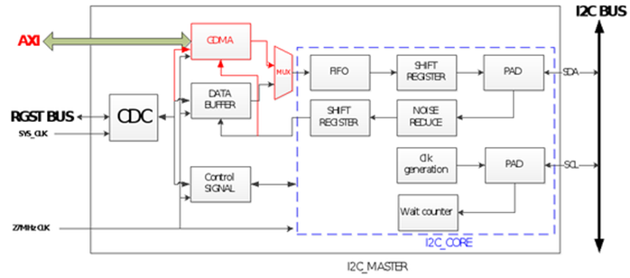
Figure 31-1 I2C MASTER Function Block
- CLOCK GENERATION: The CLK generation circuit can generate SCL signal by setting register.
- WAIT COUNTER: The wait counter circuit can detect clock stretching using SCL signal.
- SHIFT CIRCUIT: The shift circuit can send data to SDA signal, or receive data from SDA signal.
- NOISE FILTER: Noise Filter pass the signals only if the signal hold for require time. The require time can be set by register.
- DATA FIFO: The write data can save in Data FIFO then transmit to I2C slave device.
- DATA BUFFER: The DATA BUFFER module support I2C READ and I2C WRITE in normal mode.
- GDMA: GDMA module is used for DMA function, support I2C READ and I2C WRITE.
- CDC: Register CDC for clock domain crossing between 27MHz clock and SYS_CLK.
31.3 I2C Data Format
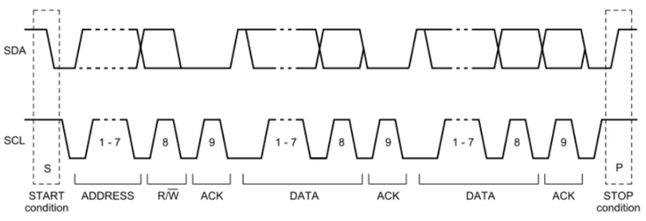
Figure 31-2 I2C Data Format
- Every byte put on the SDA line must be eight bits long
- The number of bytes that can be transmitted per transfer is unrestricted
- The first byte include 7 bits slave address and 1 bit Read(HIGH)/Write(LOW)
- START: SDA HIGH to LOW while SCL is HIGH
- STOP: SDA LOW to HIGH while SCL is HIGH
- ACK: SDA will pull LOW in the 9th clock period
- NACK: SDA will remain HIGH in the 9th clock period
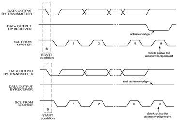
Figure 31-3 ACK and NACK condition
31.4 Clock Frequency Selection
When FREQ set to 1/2/3/4/5/6/7, it will map to divider as 1024/512/256/128/64/32/16 and the I2C clock will be 27MHz/divider. The FREQ is bit[26:24] of Group140.0 control0 register. When FREQ set to 0, then the I2C clock frequency can be set by FREQ_CUSTOM. The calculation formula is 27MHz/FREQ_CUSTOMThe FREQ_CUSTOM located in register Group140.2 (CONTROL2)[10:0].
31.5 Software Reset
A software reset can be performed by set SW_RST bit to 1. The SW_RST locate at bit15 of Group140.0 control0 register. In that case, I2C lines SCL and SDA are released. Internal states machines are reset and communication control bits, as well as status bits come back to their reset value. The configuration registers are not impacted.
31.6 NACK FLAG
When I2C master do the write transaction, the slave device is NACK. The bit0 of Group140.4 control4 register will become 1, it means I2C master write byte1 NACK. The bit1=1, means I2C master write byte2 NACK. Max can indicate 32 byte NACK. To clear the NACK flag, please set corresponding bit of Group140.3 control3 register.
31.7 I2C Operation Mode
31.7.1 Read mode & Burst Read mode
I2CM0 provides a read function. The read procedure as below:
- Set clock div value, PREFETCH=1 and SLAVE ADDR. For detailed settings, please refer to register Group140.0 (CONTROL0)[26:24], register Group140.0 (CONTROL0)[18] and register Group140.0 (CONTROL0)[7:1].
- Set the number of BYTEs that need to be read. You can set 1~65535. For detailed settings, please refer to register Group140.17 (CONTROL7)[31:16].
- If the read data is larger than 32bytes, set I2CRDATA_EN=1 (Group140.13 register).
- After receiving the interrupt, read the corresponding data.
- Clear interrupt, set I2CWRDATA_CLR=1 (Group140.12 register)
31.7.2 Write mode & Burst Write mode
I2CM0 provides a write function. The write procedure as below:
- Set clock div value, SLAVE ADDR. For detailed settings, please refer to register Group140.0 (CONTROL0)[26:24] and register Group140.0 (CONTROL0)[7:1].
- Set the number of BYTEs that need to be written. You can set 1~65535. Setting 0byte will be wrong. For detailed settings, please refer to register Group140.17 (CONTROL7)[15:0]
- Set the data to be written. Write up to 32 bytes for the first time. For detailed settings, please refer to register Group140.24-28 (DATA).
- If the data is over 32 bytes, you can set CTL_EMPTY_THRESGOLD and EMPTY_THRESHOLD_EN. For detailed settings, please refer to register Group140.8 (I2CM INT_EN0)[11:9] and Group140.8 (I2CM INT_EN0)[6].
- After triggering EMPTY_THRESHOLD_FLAG (refer to Group140.7 (INTERRUPT)[6]), read RING_VALUE (refer to Group140.5 (CONTROL5)[23:21]) to write a few 4 Bytes, or directly write the number of CTL_EMPTY_THRESGOLD*4 Bytes
- Write Group140.24 (DATA) register, 4 Bytes data at a time
- After writing, clear EMPTY_THRESHOLD_FLAG by write Group140.1 (CONTROL1)[6]=1 at first, then write Group140.1 (CONTROL1) [6]=0.
- After writing the required data, set EMPTY_THRESHOLD_EN=0.
31.7.3 Restart Mode(selective read)
I2CM0 provides the restart function that directly read after writing, and does not need to issue STOP and then START, providing the function of first write the read address and then read the data.
- You need to first set MANUAL_MODE=0 and set MANUAL_TRIG=0. For detailed settings, please refer to register Group140.9 (I2CM_MODE)[1] and Group140.9 (I2CM_MODE)[0].
- Set the number of BYTEs that need to be written and read. For detailed settings, please refer to register Group140.17 (CONTROL7)[31:16]RDCOUNT, register Group140.17 (CONTROL7)[15:0]WRCOUNT.
- Set the data to be written. For detailed settings, please refer to register Group140.24-28(DATA).
- Set clock div, PREFETCH=1, RESTART_EN=1, SUBADDR_EN=1 and SLAVE ADDR. For detailed settings, please refer to register Group140.0 (CONTROL0)[26:24], register Group140.0 (CONTROL0)[18], register Group140.0 (CONTROL0)[17], register Group140.0 (CONTROL0)[16], register Group140.0 (CONTROL0)[7:1].
- Set MANUAL_MODE =0 and set MANUAL_TRIG =1. For detailed settings, please refer to register Group140.9 (I2CM_MODE)[1] and Group140.9 (I2CM_MODE)[0].
31.7.4 I2C DMA Read Mode
The DMA read data transmission procedure is as following figure.
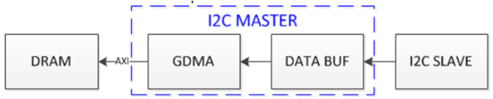
Figure 31-4 I2C DMA Read Mode
I2CM provides read from I2C slave to DRAM functionality.
- Set DMA MODE=1, refer to Group140.9 (I2CM MODE)[2].
- Set clock div value, PREFETCH and SLAVE ADDR. For detailed settings, please refer to register Group140.0 (CONTROL0)[26:24], register Group140.0 (CONTROL0)[18] and register Group140.0 (CONTROL0)[7:1].
- Set DMA destination address, refer to Group141.3 (DMA_ADR)[31:0].
- Set the number of BYTEs that the DMA needs to write. Refer to Group141.2 (DMA_LENGTH)[24:0].
- Set DMA WRITE MODE=1, DMA_GO=1, refer to Group141.1 (DMA_CONFIG)[0] and Group141.1 (DMA_CONFIG)[8].
- Set I2C_DONE_EN=0 and DMA_DONE_EN=1, refer to register Group140.8 (I2CM INT EN)[1] and Group141.6 (INT EN)[0], and wait GDMA_DONE interrupt in register Group141.5 (INT_FLAG)[0].
- Clear GDMA_DONE interrupt in register Group141.5 (INT_FLAG)[0].
31.7.5 I2C DMA Write Mode
The DMA write data reception procedure is as follows:

Figure 31-5 I2C DMA Write Mode
I2CM provides write data to I2C Slave, which data from DRAM function.
- Set DMA MODE=1, refer to Group140.9 (I2CM MODE)[2].
- Set clock div, SLAVE ADDR. For detailed settings, please refer to register Group140.0 (CONTROL0)[26:24] and register Group140.0 (CONTROL0)[7:1].
- Set DMA source address, refer to Group141.3 (DMA_ADR)[31:0].
- Set the number of BYTEs that the DMA needs to write. Refer to Group141.2 (DMA_LENGTH)[24:0].
- Set DMA WRITE MODE=0, DMA_GO=1, refer to Group141.1 (DMA_CONFIG)[0] and Group141.1 (DMA_CONFIG)[8].
- Set I2C_DONE_EN=0 and wait I2C_DONE interrupt, refer to register Group140.8 (I2CM INT EN)[1] and Group140.7 (I2CM INTERRUPT)[1].
- Clear I2C_DONE interrupt
31.7.6 I2C DMA Restart Mode
The DMA restart data reception procedure is as follows. Direction1 means write to I2C slave from register, Direction2 means read from I2C slave to DRAM.
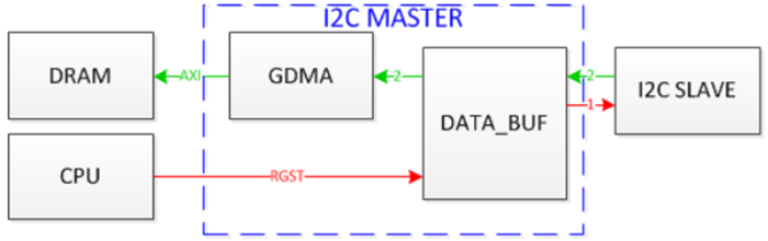
Figure 31-6 I2C DMA Restart Mode
I2CM provides restart write to I2C slave from register, read I2C slave to DRAM function.
- First set the I2C Registers
- Set DMA MODE=1, MANUAL_MODE=0, MANUAL_TRIG=0, refer to Group140.9 (I2CM MODE)[2], register Group140.9 (I2CM_MODE)[1] and Group140.9 (I2CM_MODE)[0].
- Set clock div, PREFETCH=1, RESTART_EN=1, SUBADDR_EN=1, SLAVE ADDR. For detailed settings, please refer to register Group140.0 (CONTROL0)[26:24], register Group140.0 (CONTROL0)[18], register Group140.0 (CONTROL0)[17], register Group140.0 (CONTROL0)[16], register Group140.0 (CONTROL0)[7:1]
- Set the number of BYTEs to be written. For detailed settings, please refer to register Group57.CONTROL7[31:16], register Group57.CONTROL7[15:0]
- Set the data to be written. For detailed settings, please refer to register Group140.24-28 (DATA).
- Receiver set GDMA Register
- Set DMA destination address, refer to Group141.3 (DMA_ADR)[31:0].
- Set the number of BYTEs that the DMA needs to write. Refer to Group141.2 (DMA_LENGTH)[24:0].
- Set DMA WRITE MODE=1, DMA_GO=1, refer to Group141.1 (DMA_CONFIG)[0] and Group141.1 (DMA_CONFIG)[8].
- Reset I2C Register
- Set to MANUAL_MODE=0 and set MANUAL_TRIG=1. For detailed settings, please refer to register Group140.9 (I2CM_MODE)[1] and Group140.9 (I2CM_MODE)[0].
- If the data is over 32BYTES, you can set CTL_EMPTY_THRESHOLD and EMPTY_THRESHOLD_EN. For detailed settings, please refer to register Group140.8 (I2CM INT_EN0)[11:9] and Group140.8 (I2CM INT_EN0)[6].
- After triggering EMPTY_THRESHOLD_FLAG Group140.7 (INTERRUPT)[6], read RING_VALUE Group140.5 (CONTROL5)[23:21] to write a few 4 Bytes, or directly write the number of CTL_ EMPTY_THRESHOLD *4 Bytes
- Write Group140.24 (DATA), 4 Bytes data at a time
- After writing, clear EMPTY_THRESHOLD_FLAG, write Group140.1 (CONTROL1)[6]=1, then write Group140.1 (CONTROL1) [6]=0.
- After writing the required information, set EMPTY_THRESHOLD_EN to 0.
- Set I2C_DONE_EN=0 and DMA_DONE_EN=1, refer to register Group140.8 (I2CM INT EN)[1] and Group141.6 (INT EN)[0], and wait GDMA_DONE interrupt in register Group141.5 (INT_FLAG)[0].
- Clear GDMA_DONE interrupt in register Group141.5 (INT_FLAG)[0].
31.8 FIFO Operation
The RING_VALUE shows the redundant size of the FIFO (4*n bytes) in register Group140.5 (CONTROL5)[23:21], and can set CTL_EMPTY_THRESHOLD (register Group140.8 (INT_EN0)[11:9]) and EMPTY_THRESHOLD_EN (register Group140.8 (INT_EN0)[ 6]) to trigger interrupt, then write data.The number of writing and reading bytes of FIFO is displayed by FIFO_RCOUNTER (register Group140.6 (I2CM_STATUS0)[31:16]) and FIFO_WCOUNTER (register Group140.6 (I2CM_STATUS0)[15:0]). RINC_INDEX (register Group140.7 (I2CM INTERRUPT)[21:19]) and WINC_INDEX (register Group140.7 (I2CM INTERRUPT)[18:16]) show FIFO write and read indicators.Monitor WFIFO_ENABLE (register Group140.7 (I2CM INTERRUPT)[10]), FULL_FLAG (register Group140.7 (I2CM INTERRUPT)[9]), EMPTY_FLAG (register Group140.7 (I2CM INTERRUPT)[8]) to determine if writing can continue.
31.9 Clock stretching
Detect if the slave has pulled SCL signal. If the slave is found to hold SCL signal, the master will enter the wait state, pause the transmission and send a notification. Master will wait for the slave to release SCL, then stop the transmission and wait for the next transmission. Automatic continuous transfer is not supported currently.For detailed settings, please refer to SCL_WAIT_FLAG (register Group140.7 (I2CM INTERRUPT)[7]), SCL_WAIT_INT_EN (register Group140.8 (I2CM INT_EN0)[7]), SCL_WAIT_CLR (register Group140.1 (CONTROL1)[7]), SCL_WAIT_TIME (register Group140.11 (I2CM_STATUS2)[9:0]). If you pull the Clock stretching before returning the ACK, you need to see CLK_ERR_FLAG (register Group140.7 (I2CM INTERRUPT)[2]).
31.10 I2C Interrupt Handler
I2C interrupt handler handle the internal interrupt of I2C Master Module. Group140.8 (i2cm_int_en0) register can enable interrupt for each status. An interrupt is issued when i2c active done or an interrupt is issued when FIFO data can receive or transmit data. Read Group140.7 (i2cm_interrupt) register to see what interrupt happened. After read register, need to clear interrupt flag by write Group140.1 (control1) register. I2C Master0 in IRQ number is 174, I2C Master1 in IRQ number is 175, I2C Master2 in IRQ number is 176 and I2C Master3 in IRQ number is 177.Table 31-1 shows the interrupt events in the Group140.7 (i2cm_interrupt) register.
Fields | Event flag | Interrupt event |
Bit 9 | FULL_FLAG | Monitor I2C master ring FIFO full flag. |
Bit 8 | EMPTY_FLAG | Monitor I2C master ring FIFO empty flag. |
Bit 7 | SCL_WAIT_FLAG | I2C SCL bus waits (when I2C SCL waits by I2C slave device). |
Bit 6 | EMPTY_THRESHOLD_FLAG | When I2C master ring value (read index - write index) >= empty threshold |
Bit 5 | DATA_NACK_FLAG | Monitor i2c slave, data NACK (when I2C master transmit). |
Bit 4 | ADDRESS_NACK_FLAG | Monitor i2c slave, slave address NACK (when I2C master transmit). |
Bit 3 | BUSBUSY_FLAG | When I2C master engine is idle, monitor the I2C is idle or not. |
Bit 2 | CLKERR_FLAG | I2C master active, monitor SCL input active error flag. |
Bit 1 | DONE_FLAG | I2C master active done flag. |
Bit 0 | SIFBUSY_FLAG | When I2C master engine active flag. |
Table 31-1 Interrupt Event
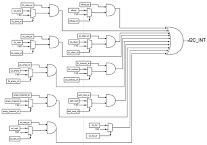
Figure 31-7 I2C Interrupt Tree
31.11 Registers Map
31.11.1 Register Memory Map
I2C Register Memory Map
Group Base Address | Data Width | Group No. | Module |
0x9C004600 | 32 | 140 | I2CM0 |
0x9C004680 | 32 | 141 | I2CM0_GDMA |
0x9C004700 | 32 | 142 | I2CM1 |
0x9C004780 | 32 | 143 | I2CM1_GDMA |
0x9C004800 | 32 | 144 | I2CM2 |
0x9C004880 | 32 | 145 | I2CM2_GDMA |
0x9C004900 | 32 | 146 | I2CM3 |
0x9C004980 | 32 | 147 | I2CM3_GDMA |
Table 31-2 I2C Register Memory Map
All I2Cs' registers have the same offset (address - base address) in corresponding I2C register group. Only I2C0 and its corresponding DMA (I2C0 DMA) registers are described in following register description, for other I2Cs (I2C1, 2, 3) please refer to I2C0 description for more detail.
31.11.2 Registers Description
I2C Register Description
RGST Table Group 140 I2C Master0
140.0 I2C Master Control 0 (control0)
Address: 0x9C004600
Reset: 0x0211 0060
Field Name | Bit | Access | Description |
RESERVED | 31:27 | RO | RESERVED |
FREQ | 26:24 | R/W | Serial bus master speed selection. 0x0: custom— customized set for I2C clock |
RESERVED | 23:19 | RU | RESERVED |
PREFETCH | 18 | R/W | Writing this bit will initiate master I2C read action, the address is set (eg. 0x10) and the corresponding data is stored in the register (eg. 0x18). |
RESTART EN | 17 | R/W | This bit determines whether the Synchronous serial in- terface's repeat start condition.(Only enable when Syn- chronous Serial interface read.) 0: disable— Do not repeat start.(default) |
SUBADDR EN | 16 | R/W | The I2C master read transaction will include device sub- address, in restart mode this bit have to set 1'b1 0: disable— skip subaddress |
SW RST | 15 | OTHER | Local reset I2C master 0: normal(default) |
RESERVED | 14:8 | RU | RESERVED |
SLAVE ADDR | 7:1 | RW | Decide serial bus slave address for the function of serial bus master (In master mode), want to access the slave device address |
RESERVED | 0 | RO | RESERVED |
140.1 I2C Master Control 1 (control1)
Address: 0x9C004604
Reset:0x0
Field Name | Bit | Access | Description |
RESERVED | 31:10 | RO | RESERVED |
I2CEMPTY CLR | 9 | WO | clear empty flag, write "1" to clear 0: none(default) |
SCL HOLD TOO LONG CLR | 8 | WO | I2c scl wait too long(when I2C scl wait by I2C slave de- vice), write "1" to clear 0: none(default) |
SCL WAIT CLR | 7 | WO | I2c scl wait (when I2C scl wait by I2C slave device), write "1" to clear 0: none(default) |
EMPTY THRESHOLD CLR | 6 | WO | I2c master fifo ring empty threshold (when I2C master empty threshold), write "1" to clear 0: none(default) |
DATA NACK CLR | 5 | WO | Monitor i2c slave, data NACK (when I2C master transm- mit), write "1" to clear 0: none(default) |
ADDRESS NACK CLR | 4 | WO | Monitor i2c slave, slave address NACK (when I2C mas- ter transmmit), write "1" to clear 0: none(default) |
BUSY CLR | 3 | WO | I2C bus busy (when I2C master is idle), write "1" to clear 0: none(default) |
CLKERR CLR | 2 | WO | Monitor the scl status when I2C master active, if the error condition occused , use this bit to clear the flag 0: none(default) |
ACTIVE CLR | 1 | WO | Done flag for i2c master read or write actions, write "1" to clear 0: none(default) |
SIFBUSY CLR | 0 | WO | I2c master start to active flag clear, write "1" to clear 0: none(default) |
140.2 I2C Master Control 2 (control2)
Address: 0x9C004608
Reset: 0x1522 07FF
Field Name | Bit | Access | Description |
RESERVED | 31 | RO | RESERVED |
SCLKI DLY5 | 30 | RW | determine scl rising trigger time delay 5T or 1T.If freq > 675KHz, sclki dly5=0 0x0: delay 1T trigger(default) |
PRE DRIVE | 29:28 | RW | Pre-drive for sub-address msb is "1" for 400K high speed mode, now don't have sub-addr, just for last read nack. 0x0: no pre-drive |
SDA DLY | 27:26 | RW | Delay the I2C sda output disable time 0x0: original— original output disable |
SCL DLY | 25:24 | RW | R/W Delay the I2C scl output disable time 0x0: original— original output disable |
SDA FILTER | 23:20 | R/W | To filter I2C sda input for bus monitor 0x0: 0 — continuous same data input |
SCL FILTER | 19:16 | R/W | To filter I2C scl input for bus monitor 0x0: 0 — continuous same data input |
RESERVED | 15:12 | RO | RESERVED |
FRQ CUSTOMDIV8 SEL | 11 | R/W | Adjust the sda active position 0: 1/2— sda start to active is middle of scl is low(default) |
FRQ CUSTOM | 10:0 | R/W | Adjust I2C clock freq when reg FREQ = 3'b000, SCL clock = 27MHz / (frq custom[10:0]+1) |
140.3 I2C Master Control 3 (control3)
Address: 0x9C00460C
Reset: 0x0
Field Name | Bit | Access | Description |
NACK CLR | 31:0 | W1C | To clear the NACK flag, write "1" to clear flag. For bust mode, |
140.4 I2C Master Control 4 (control4)
Address: 0x9C004610
Reset: 0x0
Field Name | Bit | Access | Description |
NACK FLAG | 31:0 | RO | When I2C master do the write transaction , the slave device is nack. |
140.5 I2C Master Control 5 (control5)
Address: 0x9C004614
Reset: 0x0
Field Name | Bit | Access | Description |
RESERVED | 31:24 | RO | RESERVED |
RING VALUE | 23:21 | RO | Ring Value |
STATE | 20:17 | RU | State |
RESERVED | 16 | RO | RESERVED |
PROBE MODE | 15:12 | RUW | Probe Mode |
RESERVED | 11:9 | RU | RESERVED |
SIFBUSY | 8 | RU | Sif Busy |
RESERVED | 7:0 | RU | RESERVED |
140.6 I2C Master Status 0 (i2cm status0)
Address: 0x9C004618
Reset: 0x0
Field Name | Bit | Access | Description |
FIFO RCOUNTER | 31:16 | RO | I2C master read counter |
FIFO WCOUNTER | 15:0 | RO | I2C master write counter |
140.7 I2C Master Interrupt (interrupt)
Address: 0x9C00461C
Reset: 0x8
Field Name | Bit | Access | Description |
RESERVED | 31:21 | RO | RESERVED |
RINC INDEX | 20:18 | RO | I2C master ring fifo read index |
WINC INDEX | 17:15 | RO | I2C master ring fifo write index |
RESERVED | 14:12 | RO | RESERVED |
SCL HOLD TOO LONG FLAG | 11 | RO | I2C scl bus hold low too long(I2C slave hold scl too long) 0: none(default) |
WFIFO ENABLE | 10 | RO | When I2C master ring fifo is not full,cpu can write 4 bytes data to fifo 0: none(default) |
FULL FLAG | 9 | RO | Monitor I2C master ring fifo full flag 0: none(default) |
EMPTY FLAG | 8 | RO | Monitor I2C master ring fifo empty and has error because not ready write data to i2c. 0: none(default) |
SCL WAIT FLAG | 7 | RO | I2C scl bus wait (when I2C scl wait by I2C slave device) 0: none(default) |
EMPTY THRESHOLD FLAG | 6 | RU | FIFO Empty Threshold Flag |
DATA NACK FLAG | 5 | RU | Monitor i2c slave, data NACK (when I2C master transm- mit) 0: none(default) |
ADDRESS NACK FLAG | 4 | RU | monitor i2c slave, slave address NACK (when I2C master transmmit) 0: none(default) |
BUSBUSY FLAG | 3 | RU | When I2C master engine is idle, monitor the I2C is idle or not 0: none(default) |
CLKERR FLAG | 2 | RU | I2C master active , monitor scl input active error flag 0: none(default) |
DONE FLAG | 1 | RU | I2C master active done flag 0: none(default) |
SIFBUSY FLAG | 0 | RU | When I2C master engine active flag 0: none(default) |
140.8 I2C Master Interrupt Enable (int en0)
Address: 0x9C004620
Reset: 0x0000 0800
Field Name | Bit | Access | Description |
RESERVED | 31:14 | RO | RESERVED |
SCL HOLD TOO LONG INT EN | 13 | RW | I2C slave device hold scl low too long interrupt enable 0: disable(default) |
NACK INT EN | 12 | R/W | I2C master write transaction nack interrupt enable 0: disable(default) |
CTL EMPTY THRESHOLD | 11:9 | R/W | I2C master ring fifo empty threshold control(sw control) |
EMPTY FLAG EN | 8 | R/W | I2C master ring fifo empty interrupt flag enable 0: disable(default) |
SCL WAIT INT EN | 7 | R/W | i2c slave device hold scl low interrupt enable 0: disable(default) |
EMPTY THRESHOLD EN | 6 | R/W | I2C master ring fifo empty threshold interrupt flag enable 0: disable(default) |
DATA NACK EN | 5 | R/W | I2C master write transaction nack interrupt enable 0: disable(default) |
ADDRESS NACK EN | 4 | R/W | I2C master write transaction slave address nack interrupt enable 0: disable(default) |
BUSY INT EN | 3 | R/W | i2c bus busy interrupt enable(when I2C master is idle) 0: disable(default) |
CLKERR INT EN | 2 | R/W | I2C master active , monitor scl input active error interrupt enable 0: disable(default) |
DONE INT EN | 1 | R/W | I2C master active done interrupt enable 0: disable(default) |
SIFBUSY EN | 0 | R/W | I2C master start to active interrupt enable 0: disable(default) |
140.9 I2C Master Mode Set (i2cm mode)
Address: 0x9C004624
Reset: 0x8050 8002
Field Name | Bit | Access | Description |
ADDRESS NACK STOP | 31 | RW | When address nack happened,stop the i2c master or not 0:not stop i2c master |
SCL HPERIOD | 30:20 | RW | SCL High Period Time, |
RESERVED | 19 | RO | RESERVED |
BUFPERIOD | 18:8 | RW | The setting value for the restart bus wait time, total hold time is 111ns+(37xbuf stop2start)ns |
RESERVED | 7:6 | RO | RESERVED |
EN SET HPERIOD | 5 | RW | Enable the manual set the scl high period Time 0: disable(default) |
RESERVED | 4:3 | RO | RESERVED |
I2C DMA MODE | 2 | RW | Select the DMA mode 0: ISP mode(default) |
MANUAL MODE | 1 | RW | Select the original I2C master active mode (default is 1) 0: trigger mode |
MANUAL TRIG | 0 | RW | Set the I2C master manual active when manual mode is trigger mode 0: none(default) |
140.10 I2C Master Status 1 (i2cm status1)
Address: 0x9C004628
Reset: 0x0
Field Name | Bit | Access | Description |
RESERVED | 31:16 | RO | RESERVED |
BYTE COUNTER | 15:0 | RO | I2C master write,read counter status |
140.11 I2C Master Status 2 (i2cm status2)
Address: 0x9C00462C
Reset: 0x1
Field Name | Bit | Access | Description |
RESERVED | 31:1 | RO | RESERVED |
SW RESET DONE | 0 | RO | SW RESET DONE status 0: SW RESET not DONE |
140.12 I2C Master Control 6 (control6)
Address: 0x9C004630
Reset: 0x0
Field Name | Bit | Access | Description |
I2CWRDATA CLR | 31:0 | W1C | I2C burst read ,clear the data buffer interrupt, write "1" to clear |
140.13 I2C Master Interrupt Enable 1 (int en1)
Address: 0x9C004634
Reset: 0x0
Field Name | Bit | Access | Description |
I2CRDATA EN | 31:0 | RW | I2C burst read interrupt enable 0: disable(default) |
140.14 I2C Master Status 3 (i2cm status3)
Address: 0x9C004638
Reset: 0x0
Field Name | Bit | Access | Description |
I2CRDATA FLAG | 31:0 | RO | I2C burst read ,the data buffer status flag |
140.15 I2C Master Status 4 (i2cm status4)
Address: 0x9C00463C
Reset: 0x0
Field Name | Bit | Access | Description |
I2CRD FAIL FLAG | 31:0 | RO | I2C burst read ,the data buffer overflow |
140.16 I2C Master Interrupt Enable 2 (int en2)
Address: 0x9C004640
Reset: 0x0
Field Name | Bit | Access | Description |
I2CRD FAIL INT EN | 31:0 | RW | I2C burst read ,the data buffer overflow interrupt enable 0: disable(default) |
140.17 I2C Master Control 7 (control7)
Address: 0x9C004644
Reset: 0x0001 0001
Field Name | Bit | Access | Description |
RDCOUNT | 31:16 | RW | Decide how many bytes to read |
WRCOUNT | 15:0 | RW | Decide how many bytes to write |
140.18 I2C Master Control 8 (control8)
Address: 0x9C004648
Reset: 0x6993 0005
Field Name | Bit | Access | Description |
STRETCH BUFPERIOD | 31:16 | RW | Stretch Buffer Period |
RESERVED | 15:12 | RO | RESERVED |
STRETCH TRYTIME | 11:0 | RW | Stretch count limit |
140.19 I2C Master Control 9 (control9)
Address: 0x9C00464C
Reset: 0x1
Field Name | Bit | BitAccess | Description |
RESERVED | 31:12 | RO | RESERVED |
STRETCH CNT | 11:0 | RO | Scl hold low time counter |
140.20 Reserved (reserved2)
Address: 0x9C004650
Reset: 0x0
Field Name | Bit | BitAccess | Description |
RESERVED2 | 31:24 | RO | RESERVED2 |
RESERVED2 | 23:16 | RO | RESERVED2 |
RESERVED2 | 15:8 | RO | RESERVED2 |
RESERVED2 | 7:0 | RO | RESERVED2 |
140.21 Reserved (reserved3)
Address: 0x9C004654
Reset: 0x0
Field Name | Bit | Access | Description |
RESERVED3 | 31:24 | RO | RESERVED3 |
RESERVED3 | 23:16 | RO | RESERVED3 |
RESERVED3 | 15:8 | RO | RESERVED3 |
RESERVED3 | 7:0 | RO | RESERVED3 |
140.22 Reserved (reserved4)
Address: 0x9C004658
Reset: 0x0
Field Name | Bit | Access | Description |
RESERVED4 | 31:24 | RO | RESERVED4 |
RESERVED4 | 23:16 | RO | RESERVED4 |
RESERVED4 | 15:8 | RO | RESERVED4 |
RESERVED4 | 7:0 | RO | RESERVED4 |
140.23 VERSION (version)
Address: 0x9C00465C
Reset: 0x0181 1100
Field Name | Bit | Access | Description |
ID VERSION | 31:24 | RO | id version |
DATA VERSION | 23:0 | RO | data version |
140.24 I2C Master SRAM DATA 0 to 3 (data00 03)
Address: 0x9C004660
Reset: 0x0
Field Name | Bit | Access | Description |
DATA3 | 31:24 | R/W | The data buffer3. |
DATA2 | 23:16 | R/W | The data buffer2. |
DATA1 | 15:8 | R/W | The data buffer1. |
DATA0 | 7:0 | R/W | The data buffer0. |
140.25 I2C Master SRAM DATA 4 to 7 (data04 07)
Address: 0x9C004664
Reset: 0x0
Field Name | Bit | Access | Description |
DATA7 | 31:24 | R/W | The data buffer7. |
DATA6 | 23:16 | R/W | The data buffer6. |
DATA5 | 15:8 | R/W | The data buffer5. |
DATA4 | 7:0 | R/W | The data buffer4. |
140.26 I2C Master SRAM DATA 8 to 11 (data08 11)
Address: 0x9C004668
Reset: 0x0
Field Name | Bit | Access | Description |
DATA11 | 31:24 | R/W | The data buffer11. |
DATA10 | 23:16 | R/W | The data buffer10. |
DATA9 | 15:8 | R/W | The data buffer9. |
DATA8 | 7:0 | R/W | The data buffer8. |
140.27 I2C Master SRAM DATA 12 to 15 (data12 15)
Address: 0x9C00466C
Reset: 0x0
Field Name | Bit | Access | Description |
DATA15 | 31:24 | RW | The data buffer15. |
DATA14 | 23:16 | RW | The data buffer14. |
DATA13 | 15:8 | RW | The data buffer13. |
DATA12 | 7:0 | RW | The data buffer12. |
140.28 I2C Master SRAM DATA 16 to 19 (data16 19)
Address: 0x9C004670
Reset: 0x0
Field Name | Bit | Access | Description |
DATA19 | 31:24 | RW | The data buffer19. |
DATA18 | 23:16 | RW | The data buffer18. |
DATA17 | 15:8 | RW | The data buffer17. |
DATA16 | 7:0 | RW | The data buffer16. |
140.29 I2C Master SRAM DATA 20 to 23 (data20 23)
Address: 0x9C004674
Reset: 0x0
Field Name | Bit | Access | Description |
DATA23 | 31:24 | R/W | The data buffer23. |
DATA22 | 23:16 | R/W | The data buffer22. |
DATA21 | 15:8 | R/W | The data buffer21. |
DATA20 | 7:0 | R/W | The data buffer20. |
140.30 I2C Master SRAM DATA 24 to 27 (data24 27)
Address: 0x9C004678
Reset: 0x0
Field Name | Bit | Access | Description |
DATA27 | 31:24 | R/W | The data buffer27. |
DATA26 | 23:16 | R/W | The data buffer26. |
DATA25 | 15:8 | R/W | The data buffer25. |
DATA24 | 7:0 | R/W | The data buffer24. |
140.31 I2C Master SRAM DATA 28 to 31 (data28 31)
Address: 0x9C00467C
Reset: 0x0
Field Name | Bit | Access | Description |
DATA31 | 31:24 | RW | The data buffer31. |
DATA30 | 23:16 | RW | The data buffer30. |
DATA29 | 15:8 | RW | The data buffer29. |
DATA28 | 7:0 | RW | The data buffer28. |
RGST Table Group 141 GDMA0: General DMA 0
141.0 DMA HW VER (dma hw ver)
Address: 0x9C004680
Reset: 0x018A1100
Field Name | Bit | Access | Description |
DMA HW VER | 31:0 | RO | Hardware Version A constant, usually stands for h/w delivery date, such as32'h01791000 |
141.1 DMA CONFIG (dma config)
Address: 0x9C004684
Reset: 0x00000004
Field Name | Bit | Access | Description |
Reserved | 31:9 | RO | RESERVED |
DMA GO | 8 | RUW | DMA GO Signal Write 1 to trigger DMA hardware, self clear to zero when current operation has been finished. |
Reserved | 7:3 | RO | RESERVED |
NON BUF MODE | 2 | RW | GDMA write command bufferable 0x0: all write command is bufferable |
SAME SLAVE | 1 | RW | GDMA access same slave 0x0: access different slave in SG mode(like CBDMA & DRAM at same time)(default) |
DMA MODE | 0 | RW | Set DMA Mode |
141.2 DMA LENGTH (dma length)
Address: 0x9C004688
Reset: 0x00000000
Field Name | Bit | Access | Description |
Reserved | 31:25 | RO | RESERVED |
DMA LENGTH | 24:0 | RW | Set DMA Length |
141.3 DMA ADR (dma adr)
Address: 0x9C00468C
Reset: 0x00000000
Field Name | Bit | Access | Description |
DMA SRC ADR | 31:0 | RW | DMA Source Address |
• DMA WRITE: indicate write to which main memory address • DMA READ: indicate read from which main mem- ory address Valid when DMA GO is set to 1, and can not be changed when DMA GO assert.
141.4 DMA PORT MUX (port mux)
Address: 0x9C004690
Reset: 0x00000000
Field Name | Bit | Access | Description |
Reserved | 31:1 | RO | RESERVED |
PORT MUX | 0 | RW | PORT MUX use to select PORT,ex. UART0,UART1. |
141.5 INT FLAG (int flag)
Address: 0x9C004694
Reset: 0x00000000
Field Name | Bit | Access | Description |
Reserved | 31:7 | RO | RESERVED |
LENGTH0 REG | 6 | WO | Length is zero flag • In SG MODE, if LLI RUN INDEX length is zero, theLENGTH0 REG will be 1 |
THRESHOLD REG | 5 | WO | Threshold flag • In SG MODE: when RUN LLI INDEX = THRESH- OLD LLI INDEX and NUM = THRESH- OLD NUM,the interrupt will occurs • In Normal MODE: when NUM = THRESH- OLD NUM,the interrupt will occurs |
IP TIMEOUT REG | 4 | WO | Peripheral IP Timeout When GDMA wait Peripheral IP too long will set HIGH,depend on IP TIMEOUT DEF WRITE and IP TIMEOUT DEF READ |
GDMA TIMEOUT REG | 3 | W1C | GDMA Timeout When Peripheral IP wait GDMA too long will HIGH,depend on GDMA TIMEOUT DEF WRITE GDMA TIMEOUT DEF READ |
W BYTE EN ERROR REG | 2 | W1C | Peripheral IP WRITE BYTE EN errorflag WRITE BYTE EN not meet the protocol. |
WRITE CNT | 1 | W1C | Peripheral IP DATA CNT error flag Date Count error |
DMA DONE FLAG | 0 | W1C | DMA Done If DMA done will assert this flag, write 1 clear |
141.6 DMA INT EN (dma int en)
Address: 0x9C004698
Reset: 0x00000000
Field Name | Bit | Access | Description |
Reserved | 31:8 | RO | RESERVED |
DMA IDLE EN | 7 | RW | DMA IDLE Interrupt Enable Write 1 to enable DMA IDLE interrupt function. |
LENGTH0 EN | 6 | RW | LENGTH0 Interrupt Enable Write 1 to enable LENGTH0 interrupt function. |
THRESHOLD EN | 5 | RW | THRESHOLD Interrupt Enable Write 1 to enable THRESHOLD interrupt function. |
IP TIMEOUT EN | 4 | RW | IP TIMEOUT Interrupt Enable Write 1 to enable IP TIMEOUT interrupt function. |
GDMA TIMEOUT EN | 3 | RW | GDMA TIMEOUT Interrupt Enable Write 1 to enable GDMA TIMEOUT interrupt function. |
W BYTE EN ERROR EN | 2 | RW | Write Byte ERROR Interrupt Enable Write 1 to enable WRITE BYTE ENABLE ERROR inter- rupt function |
WRITE CNT ERROR EN | 1 | RW | Write CNT ERROR Interrupt Enable Write 1 to enable WRITE CNT ERROR interrupt function |
DMA DONE EN | 0 | RW | DMA Done Interrupt Enable Write 1 to enable DMA DONE interrupt function, default is enable |
141.7 SW RESET STATE (software reset state)
Address: 0x9C00469C
Reset: 0x00000001
Field Name | Bit | Access | Description |
Reserved | 31:2 | RO | RESERVED |
SW RESET REG | 1 | RW | set Software Reset write 1 to set Software Reset |
SW RESET DONE | 0 | RO | identify SW RESET state 0x0: resetting,need wait SW RESET DONE to be HIGH 0x1: reset done,ready for SW RESET |
141.8 Reserved (reserved)
Address: 0x9C0046A0
Reset: 0x00000000
Field Name | Bit | Access | Description |
Reserved | 31:0 | RO | RESERVED |
141.9 Reserved (reserved)
Address: 0x9C0046A4
Reset: 0x00000000
Field Name | Bit | Access | Description |
Reserved | 31:0 | RO | RESERVED |
141.10 SG DMA INDEX (sg dma index)
Address: 0x9C0046A8
Reset: 0x00000000
Field Name | Bit | Access | Description |
Reserved | 31:13 | RO | RESERVED |
SG LLI RUN INDEX | 12:8 | RW | The start LLI index in a task |
Reserved | 7:5 | RO | RESERVED |
SG LLI ACCESS INDEX | 4:0 | RW | Index for LLI access Determine which LLI mapping to REG 0x0B 0x0F |
141.11 SG DMA CONFIG (sg dma config)
Address: 0x9C0046AC
Reset: 0x00000000
Field Name | Bit | Access | Description |
Reserved | 31:3 | RO | RESERVED |
SG LAST LLI IN TASK | 2 | RW | Last LLI in a task flag for LLI 0x0:when this LLI finish, execute next LLI (default) |
Reserved | 1 | RO | RESERVED |
DMA MODE | 0 | RW | Set DMA Mode for LLI 0x0: DMA WRITE (write data from Peripheral IP to main memory) |
141.12 SG DMA LENGTH (sg dma length)
Address: 0x9C0046B0
Reset: 0x00000000
Field Name | Bit | Access | Description |
Reserved | 31:25 | RW | RESERVED |
SG DMA LENGTH | 24:0 | RW | Set DMA Length for LLI |
141.13 SG DMA ADR (sg dma adr)
Address: 0x9C0046B4
Reset: 0x00000000
Field Name | Bit | Access | Description |
SG DMA ADR | 31:0 | RW | DMA Address for LLI Valid when DMA GO is set to 1, and can not be changed when DMA GO assert. |
141.14 reserve (reserve)
Address:0x9C0046B8
Reset:0x00000000
Field Name | Bit | Access | Description |
Reserved | 31:0 | RO | RESERVED |
141.15 SG SETTING (sg setting)
Address: 0x9C0046BC
Reset: 0x00000000
Field Name | Bit | Access | Description |
SG DMA ENABLE | 31 | RW | SG DMA ENABLE set SG DMA enable for LLI. |
RSV0 | 30:1 | RO | RESERVED |
SG DMA GO | 0 | RUW | SG DMA GO set SG DMA GO enable for LLI. |
141.16 THRESHOLD (threshold parameter)
Address: 0x9C0046C0
Reset: 0x00000040
Field Name | Bit | Access | Description |
THRESHOLD LLI INDEX | 31:27 | RW | THRESHOLD LLI INDEX determine the LLI index to trigger THRESHOLD INTERRUPT |
Reserved | 26:25 | RO | RESERVED |
THRESHOLD LEN | 24:0 | REW | THRESHOLD LENGTH determine the length to trigger THRESHOLD INTERRUPT. |
141.17 reserve (reserve)
Address:0x9C0046C4
Reset:0x00000000
Field Name | Bit | Access | Description |
Reserved | 31:0 | RO | RESERVED |
141.18 GDMA READ TIMEOUT (GDMA READ setting)
Address: 0x9C0046C8
Reset: 0x0010 0000
Field Name | Bit | Access | Description |
GDMA READ TIMEOUT | 31:0 | RW | GDMA READ TIMEOUT DEFINE define GDMA READ TIMEOUT counter, can not set 0. only can set when DMA GO IP=0 |
141.19 GDMA WRITE TIMEOUT (GDMA WRITE setting)
Address: 0x9C0046CC
Reset: 0x0010 0000
Field Name | Bit | Access | Description |
GDMA WRITE TIMEOUT | 31:0 | RW | GDMA WRITE TIMEOUT DEFINE define GDMA WRITE TIMEOUT counter, can not set 0. only can set when DMA GO IP=0 |
141.20 IP READ TIMEOUT (IP READ TIMEOUT setting)
Address: 0x9C0046D0
Reset: 0x0010 0000
Field Name | Bit | Access | Description |
IP READ TIMEOUT | 31:0 | RW | IP READ TIMEOUT DEFINE define IP READ TIMEOUT counter, can not set 0. only can set when DMA GO IP=0 |
141.21 IP WRITE TIMEOUT (IP WRITE TIMEOUT setting)
Address: 0x9C0046D4
Reset: 0x0010 0000
Field Name | Bit | Access | Description |
IP WRITE TIMEOUT | 31:0 | RW | IP WRITE TIMEOUT DEFINE define IP WRITE TIMEOUT counter, can not set 0. only can set when DMA GO IP=0 |
141.22 Reserved (reserved)
Address: 0x9C0046D8
Reset: 0x00000000
Field Name | Bit | Access | Description |
Reserved | 31:0 | RO | Reserved for Internal usage purpose |
141.23 Reserved (Reserved)
Address: 0x9C0046DC
Reset: 0x00000000
Field Name | Bit | Access | Description |
Reserved | 31:0 | RO | Reserved for Internal usage purpose |
141.24 WRITE DATA SLICE EMPTY (Write Data Slice Empty)
Address: 0x9C0046E0
Reset: 0x40000000
Field Name | Bit | Access | Description |
Reserved | 31 | RO | RESERVED |
W SLICE EMPTY | 30 | RO | Write Data Slice Empty or not 0x0: Write Data Slice not Empty |
Reserved | 29:0 | RO | Reserved for Internal usage purpose |
141.25 READ DATA SLICE EMPTY (Read Data Slice Empty)
Address:0x9C0046E4
Reset:0x40000000
Field Name | Bit | Access | Description |
Reserved | 31 | RO | RESERVED |
R SLICE EMPTY | 30 | RO | Read Data Slice Empty or not 0x0: Read Data Slice not Empty |
Reserved | 29:0 | RO | Reserved for Internal usage purpose |
RGST Table Group 142 I2C Master1 (Base Address: 0x9C004700, Please refer to I2C MASTER0 register offset and description for more detail)
RGST Table Group 143 GDMA1 (Base Address: 0x9C004780, Please refer to I2C GDMA0 register offset and description for more detail)
RGST Table Group 144 I2C Master2 (Base Address: 0x9C004800, Please refer to I2C MASTER0 register offset and description for more detail)
RGST Table Group 145 GDMA2 (Base Address: 0x9C004880, Please refer to I2C GDMA0 register offset and description for more detail)
RGST Table Group 146 I2C Master3 (Base Address: 0x9C004900, Please refer to I2C MASTER0 register offset and description for more detail)
RGST Table Group 147 GDMA3 (Base Address: 0x9C004980, Please refer to I2C GDMA0 register offset and description for more detail)