26. IOP8051
- edwin.chiu (Unlicensed)
- Michael Su (Unlicensed)
26.1 Introduction
There is an IOP (IO Processor) embedded inside SP7021 which is used as Processor for I/O control, IR decoding / IR wake-up and cooperation with CPU & PMC in power management purpose. The IOP core is DQ8051, so also named IOP8051, it supports dedicated JTAG debug pins which share with SP7021. In standby mode operation, the power spec reach 400uA.
.
26.2 Function Diagram
A generalized function diagram of IOP is shown in Figure 26-1.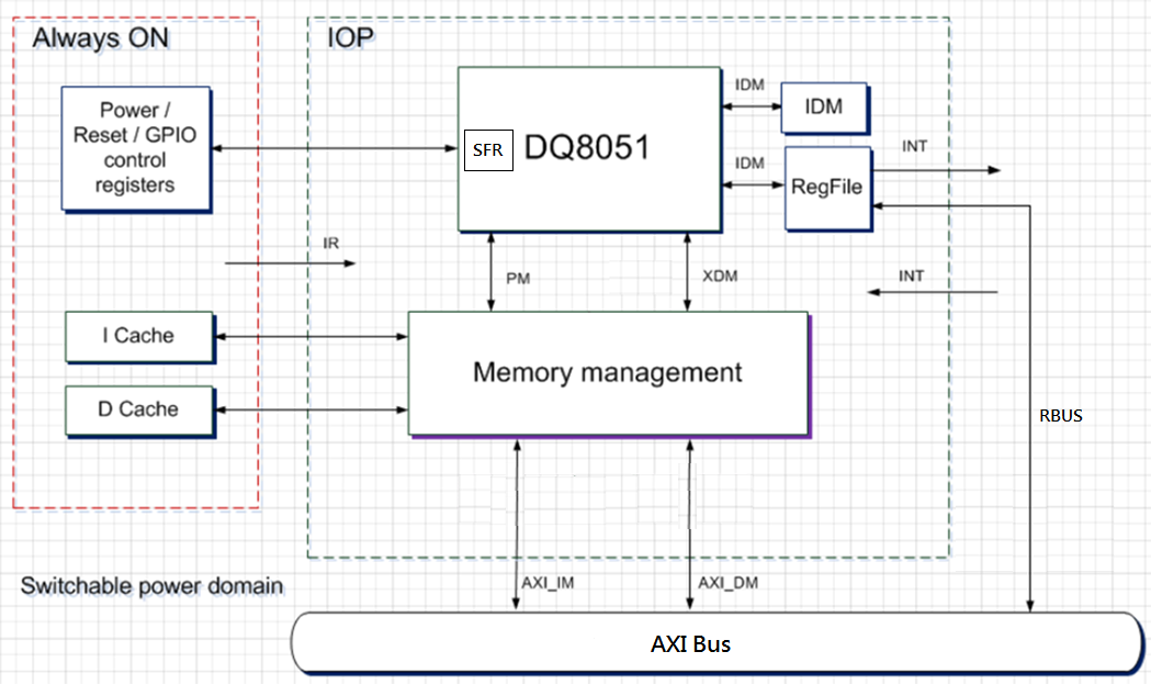
Figure 26-1 IOP Functional Blocks
- Memory management: Mainly deal with DQ8051 memory read/write access, according to its interface and address, map these operations to GPIO, registers or system memory; when access system memory can improve the performance of IOP access system memory via cache.
- RegFile: Control registers for mapping to RBUS and IOP IDM, such as mailbox registers, addressing base control registers, etc.
- SFR: SFR (Special Function registers) registers are used for power and GPIO controls.
- IR: Infrared Radiation (infrared), usually used as a remote control.
- RBUS: Main system can use this interface to control, communicate and debug IOP.
- Power Control: System standby / resume control.
- IDM: Internal data memory which the address is set between 0x30 ~ 0x6F (64B total)
- XDM: External data Memory which the address is set between 0x0000 ~ 0xFFFF. This is part of the mapped to system bus, which enables the cache to speed up execution and reduce the need for main memory access
26.3 Function Descriptions
26.3.1 Timer1 and 2
Two 16-bit timers are embedded, timer period = IOP clock cycle time. The control flow are as below.
- Set the timer in IDM: 0x3E~0x41 registers; the counter is cleared to 0x0
- Enable the timer in IDM: 0x42 register,up-counting starts
- When the timer counts to the time set, an interrupt to IOP is issued
- If the interrupt is not masked, IOP enters ISR
- IOP may clear the interrupt flag by writing "1" to the corresponding register
26.3.2 Mailbox
Mailbox is a register that can be read and written by IOP and System to exchange information with the system, faster than shared memory. The System side can be read and written by the RGST Bus. The IOP side can be accessed via the IOP_memory_management controller or via IDD memory-mapped registers - this path is still available when power down.
Note! mailbox can be read and written by System and IOP. If there is a case of writing mailbox at the same time, the write of RGST Bus is valid, and the write of IOP is ignored. Therefore, it is recommended that the use of mailbox should be one-way:
For example:
IOP Write -> System Read and Clear
System Write -> IOP Read and Clear
26.3.3 GPIO
IOP supports 128bit GPIO, which specifically supports read access to GPIO output and output enable.
26.3.4 IR
Infrared Radiation (infrared), usually used as a remote control. IR decoding is implemented by software, No hardware IR decoder is embedded
26.3.5 Reset
System may reset IOP to restart the program from the boot address. This action can be performed via RGST bus write iop_control[0]. System write 1 to iop_control[0], which asserts an IOP reset signal. This reset signal resets the IOP core, and it returns to the initial state. Caches, Timers, and other circuits are also reset.
26.3.6 Debug
- CPU can stop IOP core with an instruction breakpoint
- CPU writes an address to the breakpoint register iop_bp
- CPU writes 1 to iop_control register[2], which enables the breakpoint function
- When IOP core accesses the address that matches iop_bp, the iop_control[3] will be set to 1
- CPU also can stop IOP core with a stall control
- CPU writes 1 to iop_control register[1], which enables the stall function
- IOP core halts when this stall control bit is set to 1
- CPU uses iop_regsel to select IOP core registers for monitoring
- CPU reads iop_regout to get the values of IOP core registers for debugging
26.3.7 Interrupts to IOP
Listed below is the interrupt control register (IDM 0x39), where bit 3, 4, 5 is for software monitoring. If some restrictions are violated, the corresponding interrupt will be pulled to notify.
Bit | Description |
[0] | Timer B INT |
[1] | Timer A INT |
[2] | IR INT, this bit equals (IR_IN ^ IR_IN_POLARITY) |
[3] | Access CBUS in Power Down Mode (cache-miss occurs in power down mode) the hardware will pull the INT to notify the software that a cache miss has occurred. |
[4] | Access upper 32K IOP address region(r/w iop_addr>16'h7fff) during cache flushing if the IOP accesses the address region greater than 0x7fff, the INT will pull up. |
- IRQ for IOP core are low-level-triggered INTs
- The IRQ flags are cleared by writing "1" to them, except the IR INT
26.3.8 Interrupts from IOP
At present, the hardware directly pulls the value of this bit into SYS_INT, that is, the software fills in 1, the SYS_INT is 1, the software fills in 0, and the SYS_INT is 0. If the IOP needs to make an INT to the RISC at some point, fill in the register 1. If it is to be cleared, fill in 0.
Note: For SYS_INT registers, RISC can only perform Read and Clear operations through RGST Bus. That is, RISCx cannot set RISC_INTx to 1 by itself. Only Write 0 is valid.
26.4 System Operation
26.4.1 Initialization flow
IOP is dedicated to the processing of IO-related processors in the system, and its work needs to be controlled and coordinated by the main controllers in the system, such as RISC CPUs. The recommended software developer refers to the following IOP Core Initialization flow: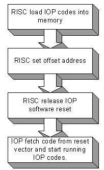
Figure 26-2 Initialization flow
26.4.2 IOP MODULE EXECUTES 8051 CODE
- Source code should reserve SDRAM memory area for IOP module code. 8051 bin file normal code and standby code can be placed in this area. The location area can be select by user.
Normal code: Monitor CPU commands.
Standby code: For RTC wake up, cooperation with CPU&PMC in power management
- When the system enters standby mode, 8051 bin file should be moved to I_Cache.
I_Cache has 16K only. Standby code cannot exceed 16K.
- When the IOP module is mounted, CPU load 8051 codes (IopNormalCode[]) into memory.
Iop_base_addr_l and iop_base_addr_h specify address.
During system boot up, when the IOP is mounted, it will load 8051 normal code and start execute 8051 code.
26.4.3 Program loader
In the system, IOP can continue to work when other modules in the system enter standby / power down modes to monitor whether the system wakes up through IR. In such a situation, the IOP will not be able to access the system memory. Therefore, the program that the IOP core needs to execute at this time, or the data segment of the operation must be stored in the cache (in the always-on power domain). The program loader is used to complete the cache fill. The implementation method is to capture the required program and data segment through memory read.
26.4.4 Power control flow
IOP supports independent operation when the system is standby / power down. When the user wakes up the system through IR, the IOP will use the power control signals to inform the system to start the relevant power management or system reset.
26.5 How To Create 8051 bin file
Please follow below steps:
Step1: Install Keil C.
Step2: Install DQ8051. (Please contact vendor(https://www.dcd.pl/product-category/cpus/) for the package)
Step3: Open project with IOP 8051 source code and edit. (Refer to figure 26-3)
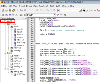
Figure 26-3 Keil C with IOP 8051 source code
Please get source code at: 8051_normal_code_20190527.rar
Step4: Generated normal bin file and put it in IopNormalCode[] which under linux/kernel/drivers/misc/iop/iopnormal.c. (Refer to figure 26-4)
When system booting, it will download this code as default setting.
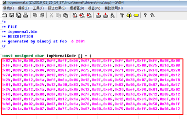
Figure 26-4 Content of iopnormal.c
Step4: Generated standby bin file and put it in IopStandbyCode[] which under linux/kernel/drivers/misc/iop/iopstandby.c.
When system enter shutdown, IOP device will call standby code to save power.
26.6 IOP8051 Module Execution
Please follow below steps:
Step1: Reserved memory for IOP module. (Refer to figure 26-5/26-6)
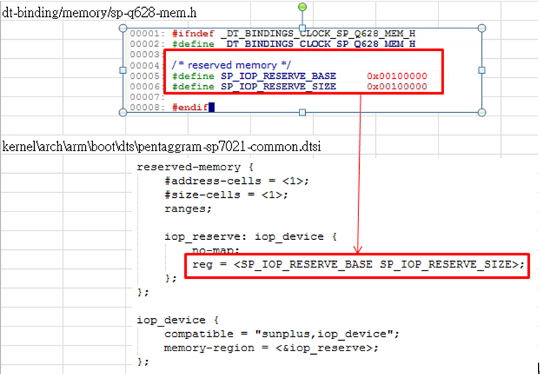
Figure 26-5 reserve memory code
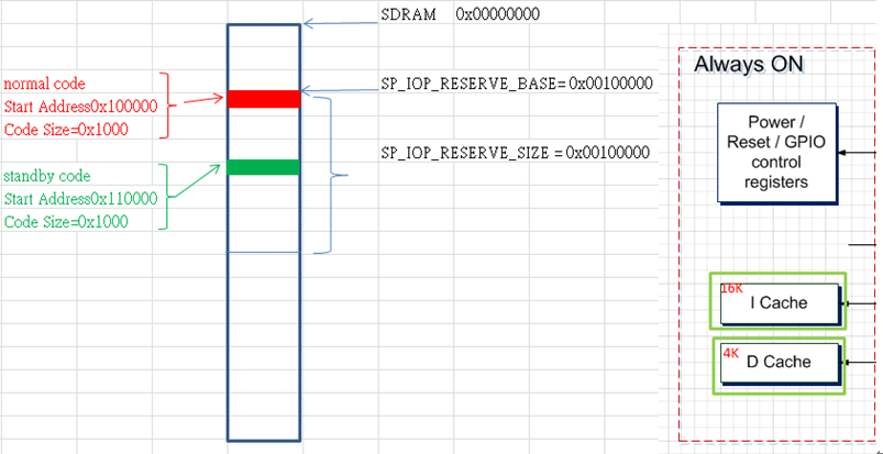
Figure 26-6 memory map
Step2: Load normal code. When the IOP module is mounted, system will load 8051 codes(IopNormalCode[]) into memory.
Below is the example code which include in the linux/kernel/drivers/misc/iop/hal_iop.c .
void hal_iop_init(void __iomem *iopbase) { regs_iop_t *pIopReg = (regs_iop_t *)iopbase; volatile unsigned int* IOP_base =(volatile unsigned int*)SP_IOP_RESERVE_BASE; unsigned char * IOP_kernel_base;
IOP_kernel_base = (unsigned char *)ioremap((unsigned long)IOP_base, IOP_CODE_SIZE); memset((unsigned char *)IOP_kernel_base,0, IOP_CODE_SIZE); memcpy((unsigned char *)IOP_kernel_base, IopNormalCode, IOP_CODE_SIZE); writel(0x00100010, (void __iomem *)(B_SYSTEM_BASE + 32*4*0+ 4*1));
pIopReg->iop_control|=0x01; pIopReg->iop_control&=~(0x8000); pIopReg->iop_control|=0x0200;//disable watchdog event reset IOP pIopReg->iop_base_adr_l = (unsigned int) ((u32)(IOP_base) & 0xFFFF); pIopReg->iop_base_adr_h =(unsigned int) ((u32)(IOP_base) >> 16); pIopReg->iop_control &=~(0x01); } EXPORT_SYMBOL(hal_iop_init); |
Step3: Load standby code. When system enters standby mode, system will load 8051 codes(IopStandbyCode[]) into memory.
Below is the example code which include in the linux/kernel/drivers/misc/iop/hal_iop.c .
void hal_iop_load_standby_code(void __iomem *iopbase)
{
regs_iop_t *pIopReg = (regs_iop_t *)iopbase;
volatile unsigned int* IOP_base =(volatile unsigned int*)(SP_IOP_RESERVE_BASE+0x10000);
unsigned char * IOP_kernel_base;
IOP_kernel_base = (unsigned char *)ioremap((unsigned long)IOP_base, IOP_CODE_SIZE);
memset((unsigned char *)IOP_kernel_base,0, IOP_CODE_SIZE);
memcpy((unsigned char *)IOP_kernel_base, SourceCode, IOP_CODE_SIZE);
writel(0x00100010, (void __iomem *)(B_SYSTEM_BASE + 32*4*0+ 4*1));
pIopReg->iop_control|=0x01;
pIopReg->iop_control&=~(0x8000);
pIopReg->iop_control|=0x0200;//disable watchdog event reset IOP
pIopReg->iop_base_adr_l = (unsigned int) ((u32)(IOP_base) & 0xFFFF);
pIopReg->iop_base_adr_h =(unsigned int) ((u32)(IOP_base) >> 16);
pIopReg->iop_control &=~(0x01);
}
EXPORT_SYMBOL(hal_iop_load_standby_code);
26.7 8051 Register Tables
26.7.1 IDM memory-mapped registers (in IOP power domain)
IDM addresses listed below are used as special function registers. The registers in 0x30~0x7F not specifically described are reserved. The other registers in 0x00~0x2F and 0x80~0xFF are for general purposes.
0x30 - 0x37 (Bank Addressing Base) | ||||
|---|---|---|---|---|
Address | Signal Name | Attribute | Reset Value | Description |
0x30 | IOP_IM_Base[7:0] | RO | 0x0 | IOP IM base address; always set to 0x0 for UVM test |
0x31 | IOP_IM_Base[15:8] | RO | 0x0 | IOP IM base address; always set to 0x0 for UVM test |
0x32 | IOP_IM_Base[23:16] | RO | 0x0 | IOP IM base address |
0x33 | IOP_IM_Base[31:24] | RO | 0x0 | IOP IM base address |
0x34 | reserved | |||
0x35 | IOP_DM_Base[23:16] | RW | 0x0 | IOP DM base address; XDM bank address when D-cache is enabled |
0x36 | IOP_DM_Base[31:24] | RW | 0x0 | IOP DM base address; XDM bank address when D-cache is enabled |
0x37 | reserved | |||
0x38 - 0x3A (Interrupt) | ||||
Address | Signal Name | Attribute | Reset Value | Description |
0x38[5:0] | IOP_INT_MASK_B | RW | 0x0 | refer to Interrupts_to_IOP |
0x39[5:0] | IOP_INT_FLAG | R/W1C | 0x0 | refer to Interrupts_to_IOP |
0x3A[0] | IOP_INT0 | RW | 0x0 | refer to Interrupts_from_IOP |
0x3A[1] | IOP_INT1 | RW | 0x0 | refer to Interrupts_from_IOP |
0x3B - 0x3C (XDM Cache Control) | ||||
Address | Signal Name | Attribute | Reset Value | Description |
0x3B[6:0] | XDM Cache_Flush_LINE_NO | RW | 0x7F | number of cache lines(32B) to be checked and then be flushed if dirty 0x0: none0x1: 2 lines are checked 0x7F(default): all lines of 4KB are checkedthis number has to be set before starting flush and not be modified until the end of flush |
0x3C[0] | XDM Cache Disable | RW | 0x0 | 0: cache is enabled (default) 1: cache is disabled |
0x3C[1] | XDM Cache Flush | RW | 0x0 | 0: normal mode write 1: flush read 1: flushing in progress (this bit is functionless when XDM cache is disabled) |
0x3C[2] | XDM Cache_DIS_CLR_V_EN | RW | 0x1 | 0: valid bits are not cleared 1: all valid bits are cleared when cache is disabled (0x3C[0]=1) (default) |
0x3C[3] | XDM Cache_DIS_CLR_D_EN | RW | 0x1 | 0: dirty bits are not cleared 1: all dirty bits are cleared when cache is disabled (0x3C[0]=1) (default) |
0x3C[4] | XDM Cache_Flush_CLR_V_EN | RW | 0x1 | 0: valid bits are not cleared 1: all valid bits are cleared when cache is flushed (0x3C[1]=1) (default) |
0x3C[5] | XDM Cache_Flush_CLR_D_EN | RW | 0x1 | 0: dirty bits are not cleared 1: all dirty bits are cleared when cache is flushed (0x3C[1]=1) (default) |
0x3C[6] | XDM Cache_all_V_set | RW | 0x0 | 0: normal function (default) 1: all valid bits are set |
0x3C[7] | XDM Cache_all_D_set | RW | 0x0 | 0: normal function (default) 1: all dirty bits are set |
0x3D (IR / RTC) | ||||
Address | Signal Name | Attribute | Reset Value | Description |
0x3D[0] | IR_O | RO | 0x0 | this bit equals IR_IN ^ IR_IN_polarity |
0x3D[1] | IR_IN_polarity | RW | 0x0 | 0: IR_O = IR_IN 1: IR_O = polarity-inverted IR_IN |
0x3D[2] | PMC_IR_LATCH | RO | 0x0 | IR_LATCH flag from PMC 1: IR wakeup |
0x3D[3] | PMC_SYS_RTC_LATCH | RO | 0x0 | SYS_RTC_LATCH flag from PMC 1: RTC wakeup |
0x3D[4] | reserved | |||
0x3D[5] | reserved | |||
0x3D[6] | CLR_PMC_IR_LATCH | W1C | 0x0 | Clear PMC_IR_LATCH in PMC |
0x3D[7] | CLR_PMC_SYS_RTC_LATCH | W1C | 0x0 | Clear PMC_SYS_RTC_LATCH in PMC |
0x3E - 0x42 (Embedded Timer) | ||||
Address | Signal Name | Attribute | Reset Value | Description |
0x3E | TIMER1[7:0] | RW | 0xFF | timer1 low byte |
0x3F | TIMER1[15:8] | RW | 0xFF | timer1 high byte |
0x40 | TIMER2[7:0] | RW | 0xFF | timer2 low byte |
0x41 | TIMER2[15:8] | RW | 0xFF | timer2 high byte |
0x42[0] | TIMER2_EN | RW | 0x0 | 1: enable 0: disable |
0x42[1] | TIMER1_EN | RW | 0x0 | 1: enable 0: disable |
0x43 - 0x48 (System Resume) | ||||
Address | Signal Name | Attribute | Reset Value | Description |
0x43 | reserved | |||
0x44[1] | DIS_SYS_RST_IOP | RW | 0x0 | disable system reset IOP; CLKISO_IOP_RST_B is blocked and can't reset IOP |
0x45 | CPU_RESUME_PCL[7:0] | RW | 0x0 | address for CPU to resume |
0x46 | CPU_RESUME_PCL[15:8] | RW | 0x0 | address for CPU to resume |
0x47 | CPU_RESUME_PCH[7:0] | RW | 0x0 | address for CPU to resume |
0x48 | CPU_RESUME_PCH[15:8] | RW | 0x0 | address for CPU to resume |
0x49 - 0x4F (INTERRUPT1, 2, 3) | ||||
Address | Signal Name | Attribute | Reset Value | Description |
0x49 | IOP_INT_MASK1_B | RW | 0x0 | Mask for INT_FLAG1 |
0x4A | IOP_INT_FLAG1 | RO | 0x0 | bit 0 : SPI_IOP_INT1_0bit 1 : SPI_IOP_INT1_1bit 2 : SPI_IOP_INT1_2bit 3 : SPI_IOP_INT1_3bit 4 : SPI_IOP_INT2_0bit 5 : SPI_IOP_INT2_1bit 6 : SPI_IOP_INT2_2bit 7 : SPI_IOP_INT2_3 |
0x4B | IOP_INT_MASK2_B | RW | 0x0 | Mask for INT_FLAG2 |
0x4C | IOP_INT_FLAG2 | RO | 0x0 |
|
0x4D | IOP_INT_MASK3_B | RW | 0x0 | Mask for INT_FLAG3 |
0x4E[2:0] | IOP_INT_FLAG3[2:0] | RO | 0x0 |
|
0x4E[7:3] | IOP_INT_FLAG3[7:3] | RO | 0x0 | bit 3 : UART_IOP_INT(UA3_INT from UART3) bit 4 : SPI_IOP_INT0_0 bit 5 : SPI_IOP_INT0_1 bit 6 : SPI_IOP_INT0_2 bit 7 : SPI_IOP_INT0_3 |
0x4F | reserved | |||
0x50 - 0x67 (Mailbox) | ||||
Address | Signal Name | Attribute | Reset Value | Description |
0x50 ~ 0x67 | Mailbox 0 ~ 11 | RW | 0x0000 | 0x50: Mailbox0[7:0]; 0x51: Mailbox0[15:8] 0x52: Mailbox1[7:0]; 0x53: Mailbox1[15:8] ... 0x64: Mailbox10[7:0]; 0x65: Mailbox10[15:8] 0x66: Mailbox11[7:0]; 0x67: Mailbox11[15:8] |
0x68 - 0x6F (RTC Timer) | ||||
Address | Signal Name | Attribute | Reset Value | Description |
0x68 | SYS_RTC_TIMER[31:24] | RO | 0x0 | System RTC timer bits 31~24 |
0x69 | SYS_RTC_TIMER[23:16] | RO | 0x0 | System RTC timer bits 23~16 |
0x6A | SYS_RTC_TIMER[15:8] | RO | 0x0 | System RTC timer bits 15~8 |
0x6B | SYS_RTC_TIMER[7:0] | RO | 0x0 | System RTC timer bits 7~0; the values(32bits) of system RTC timer (inputs of IOP) are loaded into (0x68 ~ 0x6B) only when any one address of these four registers (0x68 ~ 0x6B) is written by IOP. |
0x6C | SYS_RTC_ONTIME_SET[31:24] | RW | 0x0 | System RTC alarm setting bit 31~24 |
0x6D | SYS_RTC_ONTIME_SET[23:16] | RW | 0x0 | System RTC alarm setting bit 23~16 |
0x6E | SYS_RTC_ONTIME_SET[15:8] | RW | 0x0 | System RTC alarm setting bit 15~8 |
0x6F | SYS_RTC_ONTIME_SET[7:0] | RW | 0x0 | System RTC alarm setting bit 7~0;
|
0x70 - 0x79 (XDM 32b Data R/W) | ||||
Address | Signal Name | Attribute | Reset Value | Description |
0x70 | XDMDATA_OUT[31:24] | RW | 0x0 | XDM is originally an 8-bit data I/F, to cooperate with a 32-bit system, IOP writes out 32b data when D-cache is disabled When IOP writes XDM, the 32b data stored in these 4 registers (0x73 ~ 0x70) is written out to the 4 bytes with address[15:2] assigned by the instruction, the 8b data assigned by the instruction is dismissed. |
0x71 | XDMDATA_OUT[23:16] | RW | 0x0 | |
0x72 | XDMDATA_OUT[15:8] | RW | 0x0 | |
0x73 | XDMDATA_OUT[7:0] | RW | 0x0 | |
0x74 | XDMDATA_IN[31:24] | RO | 0x0 | XDM is originally an 8-bit data I/F, to cooperate with a 32-bit system, IOP reads in 32b data when D-cache is disabled When IOP reads XDM, besides the original byte designated by the address of the command is read, all the 4 bytes nearby with the same address[15:2] are also recorded in these 4 IDM registers (0x77 ~ 0x74) at the same time. |
0x75 | XDMDATA_IN[23:16] | RO | 0x0 | |
0x76 | XDMDATA_IN[15:8] | RO | 0x0 | |
0x77 | XDMDATA_IN[7:0] | RO | 0x0 | |
0x78 | XDM_Bank_ADR[31:24] | RW | 0x0 | XDM bank address when D-cache is disabled |
0x79 | XDM_Bank_ADR[23:16] | RW | 0x0 | XDM bank address when D-cache is disabled |
0x7A~0x7F | reserved | |||
26.7.2 SFR (in the always-on power domain)
Some SFRs are inside the DQ8051 IOP Core for core control (core SFRs); Listed below are those utilized in the peripheral design (user SFRs)
- GPIO_I[6:0], GPIO_O[6:0] and GPIO_OE[6:0] are used for the control of IV_MX[6:0] in the AO region; when main system is isolated and powered-off.
- To control IV_MX[6:0] in normal operation when system is not isolated; use GPIO_I[98:92], GPIO_O[98:92] and GPIO_OE[98:92].
To control the GPIO_P0_00~06, use the RBUS control registers
GPIO | ||||
|---|---|---|---|---|
Address | Signal Name | Attribute | Reset Value | Description |
0xEF | GPIO_I [127:120] | RO | GPIO input | General Purpose Input |
0xEE | GPIO_I [119:112] | RO | GPIO input | General Purpose Input |
0xED | GPIO_I [111:104] | RO | GPIO input | General Purpose Input |
0xEC | GPIO_I [103:96] | RO | GPIO input | General Purpose Input |
0xE7 ~ 0xE4 | GPIO_I [95:64] | RO | GPIO input | General Purpose Input |
0xDF ~ 0xDC | GPIO_I [63:32] | RO | GPIO input | General Purpose Input |
0xD7 ~ 0xD4 | GPIO_I [31:0] | RO | GPIO input | General Purpose Input |
0xCF ~ 0xC0 | GPIO_O [127:0] | RW | 0x0 | General Purpose Output |
0x9F ~ 0x98 | GPIO_OE [127:64] | RW | 0x0 | General Purpose Output Enable |
0xB7 ~ 0xB0 | GPIO_OE [63:0] | RW | 0x0 | General Purpose Output Enable |
Power | ||||
Address | Signal Name | Attribute | Reset Value | Description |
0xF4[7] | IOP_IR_SHUTDOWN_EN | RW | 0x0 | 0: Normal1: Shut down enable |
0xF4[6] | IOP_PWR_GPIO_MODE | RW | 0x0 | PWR_EN/GPIO pin is used as:0: PWR_EN(external DC_DC enable control pin; 1.2V power source for the main power domain)1: GPIO |
0xF4[5] | IOP_PWR_DWN | RW | 0x0 | 1: IOP domain power down request clear to 0 before wake-up event (EVENT_WAKEUP input) occurs by IOP_DEEP_SLEEP_RSTB |
0xF4[4] | IOP_SYSTEM_RST | RW | 0x0 | 0: Normal operation 1: System reset |
0xF4[3] | DEF_ISO | RW | 0x0 | 0: No Isolation1: Isolation |
0xF4[2] | DEF_PWR_EN_OE | RW | 0x0 | PWR_EN output enable; |
0xF4[1] | DEF_PWR_EN_O | RW | 0x0 | PWR_EN output value |
0xF4[0] | DEF_PWR_EN_I | RO | PWR_EN input value | |
0xF5[7] | MO_DC_09_ENB_ALL | RW | 0x0 | control bit output to DCDC analog macro 0: enable (default) 1: disable |
0xF5[6] | MO_DC_09_ENB_A | RW | 0x0 | control bit output to DCDC analog macro 0: enable (default) 1: disable |
0xF5[5] | MO_DC_12_ENB_ALL | RW | 0x0 | control bit output to DCDC analog macro & power_ready_check module 0: enable (default) 1: disable |
0xF5[4] | MO_DC_12_ENB_A | RW | 0x0 | control bit output to DCDC analog macro & power_ready_check module 0: enable (default) 1: disable |
0xF5[3] | MO_DC_15_ENB_ALL | RW | 0x0 | control bit output to DCDC analog macro 0: enable (default) 1: disable |
0xF5[2] | MO_DC_15_ENB_A | RW | 0x0 | control bit output to DCDC analog macro 0: enable (default) 1: disable |
0xF5[1] | REG_IOP_PWR_GATE | RW | 0x1 | 0: IOP is powered by an embedded regulator 1: IOP is powered by the same power source for main power domain (default); in QAC628, that is the DCDCs |
0xF5[0] | PWR12_READY | RO | 0: power from DCDC is not ready yet 1: power from DCDC is ready, IOP may release the isolations with SYSTEM and then wake up SYSTEM | |
26.8 IOP Registers Map
26.8.1 Registers Memory Map
Address | Group No. | Register Name | Register Description |
|---|---|---|---|
0x9C000400 | G8.0 | iop control | IOP sub-system control |
0x9C000408 | G8.2 | iop bp | IOP instruction breakpoint |
0x9C00040C | G8.3 | iop regsel | IOP register select |
0x9C000410 | G8.4 | iop regout | IOP register value |
0x9C000418 | G8.6 | iop resume pcl | IOP store pc low 2byte for system resume |
0x9C00041C | G8.7 | iop resume pch | IOP store pc high 2byte for system resume |
0x9C000420 | G8.8 | iop data0 | IOP-RISC mailbox register 0 |
0x9C000424 | G8.9 | iop data1 | IOP-RISC mailbox register 1 |
0x9C000428 | G8.10 | iop data2 | IOP-RISC mailbox register 2 |
0x9C00042C | G8.11 | iop data3 | IOP-RISC mailbox register 3 |
0x9C000430 | G8.12 | iop data4 | IOP-RISC mailbox register 4 |
0x9C000434 | G8.13 | iop data5 | IOP-RISC mailbox register 5 |
0x9C000438 | G8.14 | iop data6 | IOP-RISC mailbox register 6 |
0x9C00043C | G8.15 | iop data7 | IOP-RISC mailbox register 7 |
0x9C000440 | G8.16 | iop data8 | IOP-RISC mailbox register 8 |
0x9C000444 | G8.17 | iop data9 | IOP-RISC mailbox register 9 |
0x9C000448 | G8.18 | iop data10 | IOP-RISC mailbox register 10 |
0x9C00044C | G8.19 | iop data11 | IOP-RISC mailbox register 11 |
0x9C000450 | G8.20 | iop base adr l | IOP base address[31:16] |
0x9C000454 | G8.21 | iop base adr h | IOP base address[15:0] |
0x9C000458 | G8.22 | Memory bridge control | Memory bridge control |
0x9C00045C | G8.23 | iop remap adr l | IOP remapping base address[15] |
0x9C000460 | G8.24 | iop remap adr h | IOP remapping base address[31:16] |
0x9C000464 | G8.25 | iop direct adr | IOP direct address[15:0] |
26.8.2 Registers Description
RGST Table Group 8 IO Processor
8.0 IOP sub-system control (iop control)
Address: 0x9C000400
Reset: 0x6011
Field Name | Bit | Access | Description |
DIS SYS RST IOP | 15 | RW | Disable System Reset IOP |
Reserve | 14 | RO | |
|
|
|
|
Reserve | 12 | RO | |
|
|
|
|
IOP SSTL RET EN1 | 10 | RW | DDR1 IO Retention Control Signal |
IOP WATCH DOG RST EN | 9 | RW | Disable watch-dog reset event to reset IOP |
IOP SSTL RET EN0 | 8 | RW | DDR0 IO Retention Control Signal |
RISC INTB | 7 | W1C | IOP to System Interrupt B |
RISC INTA | 6 | W1C | IOP to System Interrupt A |
NMIR | 5 | RW | X NMI edge control |
| NMIF | 4 | RW | X NMI edge control Falling edge 0: inactive 1: active(default) |
| BPS | 3 | RW | IOP break-point stopped flag 0: IOP is not stopped(default) 1: IOP is stopped at break-point now. |
| BPE | 2 | RW | IOP break-point control 0: Break-point disabled(default) 1: Enable break-point. When IOP execute to the break- point, it will assert BPS. |
| ST | 1 | RW | IOP stall control 0: IOP running normally(default) 1: IOP is stalled(for debugging or updating new firmware) |
| RST | 0 | RW | IOP reset control 0: release(default) 1: assert |
8.2 IOP instruction breakpoint (iop bp)
Address: 0x9C000408
Reset: 0xFFFF
Field Name | Bit | Access | Description |
| BP | 15:0 | RW | IOP instruction break-point address. |
8.3 IOP register select (iop regsel)
Address: 0x9C00040C
Reset: 0x0000
Field Name | Bit | Access | Description |
| REGSEL | 15:0 | RW | Select IOP register 0x0: Opcode(default) 0x1: PCH register 0x2: PCL register 0x3: A register 0x4: X register 0x5: Y register 0x6: S register 0x7: PSR register others: reserved |
8.4 IOP register value (iop regout)
Address: 0x9C000410
Reset: 0x0000
Field Name | Bit | Access | Description |
| REGOUT | 15:0 | RO | IOP register window. Use REGSEL to select register to read |
8.6 IOP store pc low 2byte for system resume (iop resume pcl)
Address: 0x9C000418
Reset: 0x0000
Field Name | Bit | Access | Description |
| IOP RESUME PCL | 15:0 | RW | RISC Resume PC Low IOP store system program counter low 2byte for system resume. |
8.7 IOP store pc high 2byte for system resume (iop resume pch)
Address: 0x9C00041C
Reset: 0x0000
Field Name | Bit | Access | Description |
| IOP RESUME PCH | 15:0 | RW | RISC Resume PC High IOP store system program counter high 2byte for system resume. |
8.8 IOP-RISC mailbox register 0 (iop data0)
Address: 0x9C000420
Reset: 0x0000
Field Name | Bit | Access | Description |
| IOP DATA0 | 15:0 | RW | IOP DATA0 |
8.9 IOP-RISC mailbox register 1 (iop data1)
Address: 0x9C000424
Reset: 0x0000
Field Name | Bit | Access | Description |
| IOP DATA1 | 15:0 | RW | IOP DATA1 |
8.10 IOP-RISC mailbox register 2 (iop data2)
Address: 0x9C000428
Reset: 0x0000
Field Name | Bit | Access | Description |
| IOP DATA2 | 15:0 | RW | IOP DATA2 |
8.11 IOP-RISC mailbox register 3 (iop data3)
Address: 0x9C00042C
Reset: 0x0000
Field Name | Bit | Access | Description |
| IOP DATA3 | 15:0 | RW | IOP DATA3 |
8.12 IOP-RISC mailbox register 4 (iop data4)
Address: 0x9C000430
Reset: 0x0000
Field Name | Bit | Access | Description |
| IOP DATA4 | 15:0 | RW | IOP DATA4 |
8.13 IOP-RISC mailbox register 5 (iop data5)
Address: 0x9C000434
Reset: 0x0000
Field Name | Bit | Access | Description |
| IOP DATA5 | 15:0 | RW | IOP DATA5 |
8.14 IOP-RISC mailbox register 6 (iop data6)
Address: 0x9C000438
Reset: 0x0000
Field Name | Bit | Access | Description |
| IOP DATA6 | 15:0 | RW | IOP DATA6 |
8.15 IOP-RISC mailbox register 7 (iop data7)
Address: 0x9C00043C
Reset: 0x0000
Field Name | Bit | Access | Description |
| IOP DATA7 | 15:0 | RW | IOP DATA7 |
8.16 IOP-RISC mailbox register 8 (iop data8)
Address: 0x9C000440
Reset: 0x0000
Field Name | Bit | Access | Description |
| IOP DATA8 | 15:0 | RW | IOP DATA8 |
8.17 IOP-RISC mailbox register 9 (iop data9)
Address: 0x9C000444
Reset: 0x0000
Field Name | Bit | Access | Description |
| IOP DATA9 | 15:0 | RW | IOP DATA9 |
8.18 IOP-RISC mailbox register 10 (iop data10)
Address: 0x9C000448
Reset: 0x0000
Field Name | Bit | Access | Description |
| IOP DATA10 | 15:0 | RW | IOP DATA10 |
8.19 IOP-RISC mailbox register 11 (iop data11)
Address: 0x9C00044C
Reset: 0x0000
Field Name | Bit | Access | Description |
| IOP DATA11 | 15:0 | RW | IOP DATA11 |
8.20 IOP base address[31:16] (iop base adr l)
Address: 0x9C000450
Reset: 0x0000
Field Name | Bit | Access | Description |
| IOP OFFSET L | 15:5 | RW | IOP base address[15:5] NOTE: IOPbaseaddress= IOP OFFSET H concatenate IOP OFFSET L . |
| Reserve | 4:0 | RO |
8.21 IOP base address[15:0] (iop base adr h)
Address: 0x9C000454
Reset: 0x0000
Field Name | Bit | Access | Description |
| IOP OFFSET H | 15:0 | RW | IOP base address[31:16] NOTE: IOPbaseaddress = IOP OFFSET H concatenate IOP OFFSET L . |
8.22 Memory bridge control (Memory bridge control)
Address: 0x9C000458
Reset: 0x0000
Field Name | Bit | Access | Description |
| MEMORY IOP EN | 1 | RO | IOP self-enabled Memory address remapping status 0: IOP disabled Memory remapping(default) 1: IOP enabled Memory remapping |
MEMORY RISC EN | 0 | RW | RISC enable Memory address remapping 0: RISC disabled Memory remapping(default) 1: RISC enabled Memory remapping NOTE: Both MEMORY IOP EN and MEMORY RISC EN should be 1 to enable 32-bit addressing mode |
8.23 IOP remapping base address[15] (iop remap adr l)
Address: 0x9C00045C
Reset: 0x0000
Field Name | Bit | Access | Description |
| IOP OFFSET2 L | 0 | RO | IOP remapping base address[15] NOTE: IOP remapping base address = {IOP OFFSET2 H,IOP OFFSET2 L, 15-bit 0} . (for 32-bit addressing mode) |
8.24 IOP remapping base address[31:16] (iop remap adr h)
Address: 0x9C000460
Reset: 0x0000
Field Name | Bit | Access | Description |
| IOP OFFSET2 H | 15:0 | RO | IOP remapping base address[31:16] NOTE: IOP remapping base address = {IOP OFFSET2 H,IOP OFFSET2 L, 15-bit 0} (for 32-bit addressing mode) |
8.25 IOP direct address[15:0] (iop direct adr)
Address: 0x9C000464
Reset: 0x0000
Field Name | Bit | Access | Description |
| IOP DIRECT ADR | 15:0 | RW | IOP direct access address[15:0] NOTE: IOP use this register to use Indirect Y adderss mode access, RISC can direct set this address. |