23. BCH
- edwin.chiu (Unlicensed)
23.1 Introduction
The physical characteristics of Nand Flash make a certain probability of error in the data reading and writing process, so there must be a corresponding error detection and correction mechanism, so the ECC(Error Checking and Correction Code) is used for data error detection and correction. Nand Flash ECC, common algorithms are Hamming code and BCH(Bose–Chaudhuri–Hocquenghem codes). The implementation of such algorithms can be software or hardware. SP7021 implements a hardware BCH for this usage.
The BCH algorithm is usually implemented by the corresponding Nand Flash controller, including the corresponding hardware BCH ECC module, and implements the BCH algorithm. As a software aspect, it is necessary to operate the corresponding BCH-related before reading the data and before writing the data. The register is set to BCH mode, and then the corresponding BCH status register is read to know if there is an error, and the generated BCH check code is used for writing.
The BCH IP is a BCH engine for BCH encode/decode with 14-level BCH algorithms. It can fetch data from system memory for encode/decode and write the result back to the system memory. The Memory is used to storage the data transferred. A NAND device is the data storage unit, which can be accessed by the NAND-Flash controller by a group of signals with proper NAND-Flash interface timing. All the function units communicate through the AXI BUS. Software can select auto encode/decode or manual trigger encode/decode mode.
23.2 Function Diagram
A generalized hardware block diagram of BCH is shown in Figure 23-1.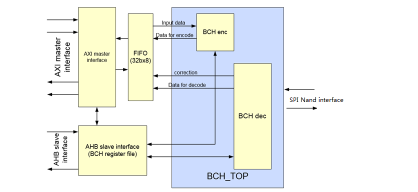
Figure 23-1 BCH Hardware Block Diagram
- BCH enc: BCH enc is used for BCH encode with 14-level BCH algorithms.
- BCH dec: BCH dec is used for BCH decode with 14-level BCH algorithms.
- AXI master: AXI master is used to transfer data for encode/decode with memory through AXI BUS.
- AHB slave: AHB slave is used to config register file through AHB-lite BUS. CPU can write register in this module through AHB-lite Bus to config function in BCH IP. See the Register chapter for details
23.3 Data Structure
Table 23-1 shows the relationship of ECC data spec, Parity data length and Protect software use byte.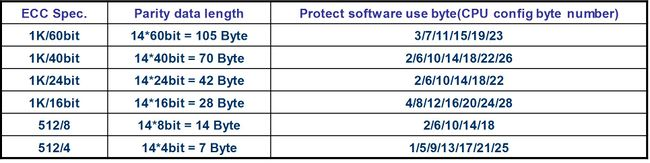
Table 23-1 ECC Data Format
"1KB/60bit" means the correct ability is 60bit within 1K byte date, "1KB/40bit" means the correct ability is 40bit within 1K byte date and so on.
The sum of the parity and SW protected data must be 4-byte align. The figure 22-2 is the example of ECC spec. as 1K/16b and software protected byte as 4 bytes case.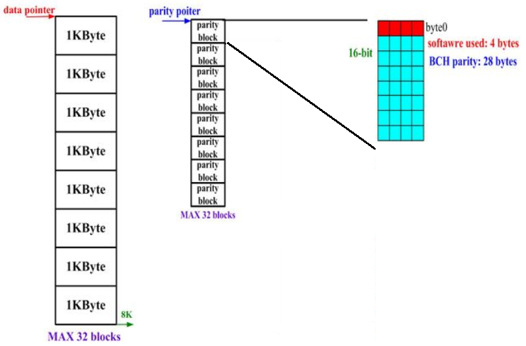
Figure 23-2 Software Protect Date Size
23.4 Auto BCH Enable
Set register Group 87.16 spi_bch bit4 to 1, it will enable auto BCH mode. Please refer to 22.6.2 registers description for more detail description.
23.5 BCH Interrupts
There are two kinds of interrupt.
Decode fail Interrupt is issued when bch can't fix data because too much error bits happens and Decode fail mask is true. Finish interrupt is issued when bch work finish and Finish mask is true.
Figure 23-3 shows the BCH interrupt tree.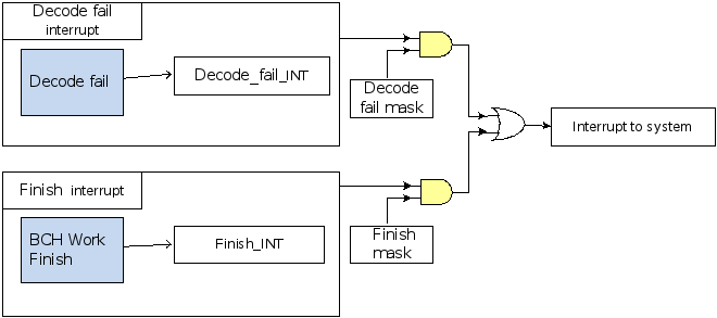
Figure 23-3 BCH Interrupt Tree
23.6 Registers Map
23.6.1 Registers Memory Map
BCH Group 0 BCH Controller
Address | Group No. | Register Name | Register Description |
0x9C101000 | G0.0 | configuration | bch control register |
0x9C101004 | G0.1 | data pointer | bch encode/decode data start address |
0x9C101008 | G0.2 | parity pointer | bch encode/decode parity start address |
0x9C10100C | G0.3 | Interrupt status | bch interrupt, write 1 clear |
0x9C101010 | G0.4 | Software clear flag | write 1 to reset bch |
0x9C101014 | G0.5 | Interrupt mask | bch interrupt mask control register |
0x9C101018 | G0.6 | Report status | bch report status |
0x9C10101C | G0.7 | Sector error report | report the Nth (N=0˜31) block has error bit or not |
0x9C101020 | G0.8 | Sector fail report | report the Nth (N=0˜31) block has to much error bits can't be fixed by decoder |
0x9C10102C | G0.11 | Control register | The controller register for ff&00 check and correction method |
RGST Table Group 87 SPI NAND Controller Registers
Address | Group No. | Register Name | Register Description |
| 0x9C002BC0 | G87.16 | spi_bch | SPI BCH configuration Register |
23.6.2 Registers Description
BCH Group 0 BCH Controller
0.0 bch control register (configuration)
Address: 0x9C101000
Reset: 0x0
Field Name | Bit | Access | Description |
| Reserved | 31 | RO | |
| Software byte | 30:28 | RW | Software protected byte 0x0: 3 byte for 1KB/60-b; 2(1KB/40); 2(1KB/24); 4(1KB/16); 2(512B/8); 1(512B/4) (default) 0x1: 7 byte for 1KB/60-b; 6(1KB/40); 6(1KB/24); 8(1KB/16); 6(512B/8); 5(512B/4) 0x2:11 byte for 1KB/60-b; 10(1KB/40); 10(1KB/24); 12(1KB/16); 10(512B/8); 9(512B/4) 0x3:15 byte for 1KB/60-b; 14(1KB/40); 14(1KB/24); 16(1KB/16); 14(512B/8); 13(512B/4) 0x4:19 byte for 1KB/60-b; 18(1KB/40); 18(1KB/24); 20(1KB/16); 18(512B/8); 17(512B/4) 0x5:23 byte for 1KB/60-b; 22(1KB/40); 22(1KB/24); 24(1KB/16); NA(512B/8); 21(512B/4) 0x6:NA for 1KB/60-b; 26(1KB/40); NA(1KB/24); 28(1KB/16); NA(512B/8); 25(512B/4) others: reserved |
| Reserved | 27:26 | RO | |
Correction priority | 25:24 | RW | Set the correction request priority |
bit24 0: correct>data (default) | |||
Reserved | 23:21 | RO | |
Sector number | 20:16 | RW | Set the number N of block (1block=1K Byte) |
Reserved | 15:12 | RO | |
Data mode | 11 | RW | 32byte or 16byte alignment |
Correct mode | 10:8 | RW | Correct mode |
Reserved | 7:5 | RO | |
Encode Decode | 4 | RW | Encode/Decode |
Reserved | 3:2 | RO | |
Start trigger | 1 | RUW | Config done |
Start trigger | 0 | RUW | Start trigger |
0.1 bch encode/decode data start address (data pointer)
Address: 0x9C101004
Reset: 0x0
Field Name | Bit | Access | Description |
Data pointer | 31:2 | RW | bch data pointer address, align to word(4 bytes) bit[1:0] |
Data pointer | 1:0 | RO | bch data pointer address[1:0] always 0x0 |
0.2 bch encode/decode parity start address (parity pointer)
Address: 0x9C101008
Reset: 0x0
Field Name | Bit | Access | Description |
Parity pointer | 31:2 | RW | bch parity pointer address, align to word(4 bytes) bit[1:0] |
Parity pointer | 1:0 | RO | bch parity pointer address[1:0] always 0x0 |
0.3 bch interrupt, write 1 clear (Interrupt status)
Address: 0x9C10100C
Reset: 0x0
Field Name | Bit | Access | Description |
| Reserved | 31:21 | RO | |
| Correct number | 20:16 | RO | corrected block number counter |
| Reserved | 15:13 | RO | |
| Current number | 12:8 | RO | data block number counter |
| Reserved | 7:5 | RO | |
| Busy | 4 | RU | Busy flag, pull high when start trigger and pull low when work finish |
| Reserved | 3:1 | RO | |
| Bch interrupt | 0 | EUW | bch interrupt register, write 1 clear |
0.4 write 1 to reset bch (Software clear flag)
Address: 0x9C101010
Reset: 0x0
Field Name | Bit | Access | Description |
| Reserved | 31:1 | RO | |
| Clr flag | 0 | RUW | User writes 1 to reset bch, it will return to 0 when reset finished |
0.5 bch interrupt mask control register (Interrupt mask)
Address: 0x9C101014
Reset: 0x0
Field Name | Bit | Access | Description |
| Reserved | 31:2 | RO | |
| Decode fail mask | 1 | RW | 1/0: while bch can't fixed data because too much error bits happens, interrupt asserts or not 0: not mask (default) 1: mask |
| Finish mask | 0 | RW | 1/0: when bch work finish, interrupt asserts or not 0: not mask (default) 1: mask |
0.6 bch report status (Report status)
Address: 0x9C101018
Reset: 0x1100 0000
Field Name | Bit | Access | Description |
Reserved | 31:29 | RO | |
|
|
|
|
Reserved | 27:25 | RO | |
|
|
|
|
Reserved | 23:19 | RO | |
| Error count | 18:8 | RO | Counttotalerrorbit ofthiswork,maxi- mum=60*32=1920bits |
| Reserved | 7:5 | RO | |
| Decode fail | 4 | RO | bch decoder fail or not,write 1 clear decode fail interrupt 0: decode success (default) |
| Reserved | 3:1 | RO | |
| Finish | 0 | RO | bch encode/decode finish,write 1 clear finish interrupt 0: not finish (default) 1: finish |
0.7 report the Nth (N=0˜31) block has error bit or not (Sector error report)
Address: 0x9C10101C
Reset: 0x0
Field Name | Bit | Access | Description |
| Sector error | 31:0 | RO | It represents the error block of this work Note the error block still can be corrected by bch, when can't corrected, "decoder fail" will assert EX: bit0: 1st block has error or not bit1: 2nd block has error or not 32'hFFFF 0000: block 1˜16 has no errors block 17˜32 has errors |
0.8 report the Nth (N=0˜31) block has to much error bits can't be fixed by decoder
(Sector fail report)
Address: 0x9C101020
Reset: 0x0
Field Name | Bit | Access | Description |
| Sector decode fail | 31:0 | RO | It represents decoded fail block of this work EX: bit0: 1st block decode fail or not bit1: 2nd block decode fail or not 32'hFFFF 0000: block 1˜16 decode success block 17˜32 decode fail |
0.11 The controller register for ff&00 check and correction method (Control register)
Address: 0x9C10102C
Reset: 0x4
Field Name | Bit | Access | Description |
| Reserved | 31:3 | RO | |
| Last corr nonbufw | 2 | RW | Just the last sector use nonbufferable write 0: encode:all sectors use nonbufferable write for all the en- parity write; decode:all sectors use nonbufferable write for all correc- tion write(please set to '0' in decode mode); 1: encode:only last sector use nonbufferable write for en- parity(default) decode:not allowed |
| Reserved | 1:0 | RO |
RGST Table Group 87 SPI NAND Controller Registers
87.16 SPI BCH configuration Register (spi bch)
Address: 0x9C002BC0
Reset: 0x0000
Field Name | Bit | Access | Description |
| Reserved | 31:16 | RO | Default to be zero |
| BCH DATA LEN | 15:8 | RW | For bch data: 0x0: 0Byte parity data per BCH sector 0x1: 1Byte parity data per BCH sector ... 0xff: 255Byte parity data per BCH sector |
| Reserved | 7 | RO | Default to be zero |
| BCH DATA MODE | 6 | RW | BCH data mdoe select 0: 512Byte per BCH. 1: 1k Byte per BCH. |
| BCH ACC | 5 | RW | 32Byte or 16Byte align 0: 32Byte align. 1: 16Byte align. |
| AUTO BCH EN | 4 | RW | Auto BCH function enable Write 1 enable. It will encode data before the page program or decode data during page read. |
| SECTOR NUM | 3:0 | RW | Set the number N of block for BCH N= 0˜15(1˜16 blocks) |