25. CBDMA
- edwin.chiu (Unlicensed)
- Michael Su (Unlicensed)
25.1 Introduction
The CB_DMA provides CBUS (CPU Bus) MASTER storage space for use as DATA RAM, and also provides DMA function. DATA RAM can be used without any settings, and reading and writing is very efficient. Both d DATA RAM and CACHE are two forms of on-chip memory. The goal is to improve system performance (read-write speed is faster than DRAM), but the implementation is completely different. The cache is fully automatic. Software colleagues can be used as no such hardware. For data ram, software needs to specify the location to access.
Data ram In addition to the temporary storage data in operation, another function is to let the system have some place to store the data before the system has been initialized. In addition, this hardware also provides DMA function, which is quite flexible. Let software In the future, there is an opportunity to use hardware acceleration in critical places to perform memset, read/write/move the flexibility of large amounts of data.
SP7021 CB_DMA support internal SRAM that size is 128Kbytes. CB_DMA is accessed by DMA_CTRL (master) and also access to DRAM (slave). CB_DMA also support security function.
The control registers locate at RGST table Group 26 which memory map in 0x9C000D00~0x9C000D7F.
25.2 Function Diagram
The function diagram of CBDMA is shown in Figure 25-1.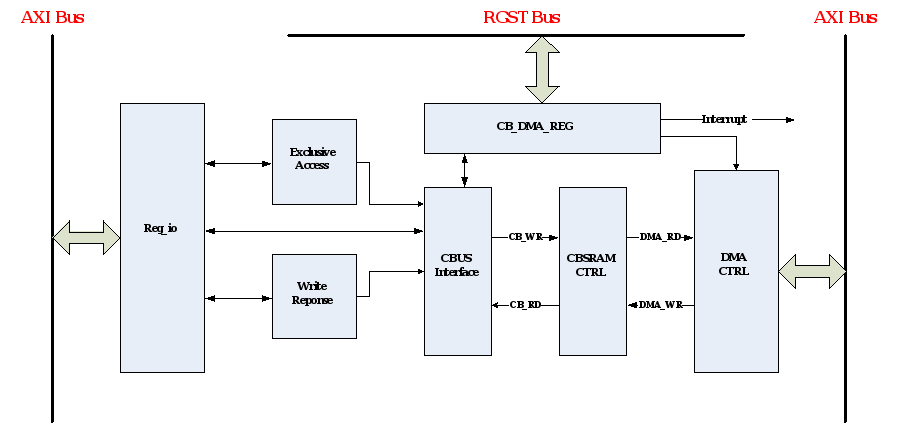
Figure 25-1 CBDMA Functional Blocks
- REG_IO: Judging by the AXI command coming in from the slave end, when read / write is interleaved, there is a corresponding arbitration mechanism to determine which read / write command is first served.
- Exclusive access: The CB_DMA slave side supports AXI Exclusive access, but only supports it at most once.
- Write response: The write command is received by the slave side, and the feedback will be sent when the wdata is received.
- CB_DMA_REG: HE_RGST BUS slave, used to control the internal settings of register.
- CBUS interface: Receive the command sent by the BUS master and convert it to the interface of CBSRAM_CTRL to access CBSRAM.
- CBSRAM_CTRL: As Internal SRAM, the CBDMA slave / master may be accessed at the same time, so it needs to be arbiration. The priority of the slave is defined to be greater than the master.
- DMA_CTRL: As the master, parse the DMA settings issued by CB_DMA_REG and convert them to AXI command to send them out.
25.3 System Operation Mode
CMD_QUE_DEPTH, MEMSET_VALUE, DMA_MODE, DMA_LENGTH, DMA_SRC_ADR and DMA_DES_ADR cannot be changed during DMA_GO == 1. If it is violated, H/W can self-protect, and the software will not be written in until DMA_GO = 0, which can be determined by a bit. Owner. The Semaphore mechanism may be safer and better.
CMD_QUE_DEPTH, MEMSET_VALUE, DMA_MODE, DMA_LENGTH, DMA_SRC_ADR, DMA_DES_ADR and DMA_GO parameters are defined in registers map segments.
25.3.1 MEMSET Mode
- Set below registers:
- dma_mode: Set dma_mode to MEMSET mode
- memset: Value is the value you want to fill in main memory.
- Length: The number of bytes to memset this time.
- Dest Addr: The number of bytes to memset this time.
- Src addr[1:0]: The offset of memset data.
- After DMA Go, the result will be the memset value filled to Dest Addr, totally filled "length" byte.
- Write data flow :
Please refer figure 25-2 Step8 ~ step9.
25.3.2 DMA Write Mode
- Set below registers:
- dma_mode: Set dma_mode to DMA Write mode.
- Length: The number of bytes to be transferred from CBSRAM Write to SDRAM this time.
- Dest Addr: Write out data into DRAM address.
- Src Addr: From which address of CBSRAM, read data and write to DRAM.
- After DMA Go, CB_DMA will move data from the CBSRAM of Src_Addr to the SDRAM starting with Dest_Addr, with a total of "length" bytes. DMA_DONE_FLAG will be set after Write ends. If the interrupt of DMA_DONE is not masked, there will be an interrupt of DMA_DONE.
- Write data flow :
Please refer figure 25-2 Step1 ~ step5.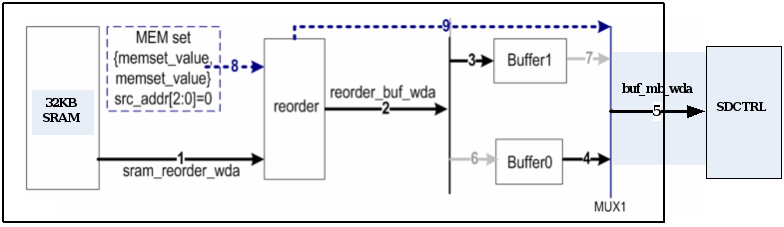
Figure 25-2 Write Data Flow
25.3.3 DMA Read Mode
- Set below registers:
- dma_mode: Set dma_mode to DMA Read mode.
- Length: The number of bytes to be returned from DRAM read this time.
- Dest Addr: Read back data into the address of CBSRAM.
- Src Addr: Read data from which address of DRAM.
- After DMA Go, CB_DMA will move data from the SDRAM of Src_Addr to the CBSRAM starting with Dest_Addr, for a total of "length" bytes. After the Read ends, DMA_DONE_FLAG will be set to 1. If the interrupt of DMA_DONE is not masked, there will be an interrupt of DMA_DONE.
- Read data flow :
Please refer figure 25-3 Step1 ~ step5. 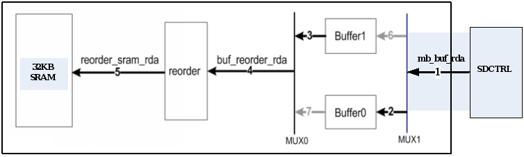
Figure 25-3 Read Data Flow
25.3.4 DMA Copy Mode
- Set below registers:
- dma_mode: Set dma_mode to DMA Copy mode.
- Length: The number of bytes to copy.
- Dest Addr: Copy the data into the address of the DRAM.
- Src Addr: Read the data from the address of the DRAM and write it to Dest DRAM.
- After DMA Go, CB_DMA will move data from the DRAM of Src_Addr to the DRAM starting with Dest_Addr, for a total of "length" bytes. After the copy ends, DMA_DONE_FLAG will be set to 1. If the interrupt of DMA_DONE is not masked, there will be an interrupt of DMA_DONE.
- The last 256 bytes inside CB_DMA will be treated as buffer and the contents will be destroyed.
- Copy data flow :
Please refer figure 25-4 Step1 ~ step9.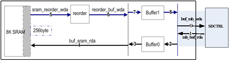
Figure 25-4 Copy Data Flow
25.3.5 SG(Scatter-gather) DMA Mode
The SG DMA mode is like auto repeat mode of MEMSET or DMA write or DMA read or DMA copy. Through this function, user can read several area data and write to a gather area. User also can read data in a continue area and write to several discontinue area. The max operation times is 32. The control registers are G26.10~15. Below shows the registers setting flow for continue DMA copy:
- Set below registers:
- LLI_ACCESS_INDEX: Determine which LLI(Link List Item) mapping to following registers.
- LAST_LLI_IN_TASK: If this flag setup, it indicate the last LLI.
- dma_mode: Set dma_mode to DMA Copy mode.
- Length: The number of bytes to copy.
- Dest Addr: Copy the data into the address of the DRAM.
- Src Addr: Read the data from the address of the DRAM and write it to Dest DRAM.
- Repeat above action.
- After SG DMA Go, CB_DMA will move data from the DRAM of Src_Addr to the DRAM starting with Dest_Addr according index. After the copy ends, DMA_DONE_FLAG will be set to 1. If the interrupt of DMA_DONE is not masked, there will be an interrupt of DMA_DONE.
Figure 25-5 shows an example of SG DMA with DMA copy mode
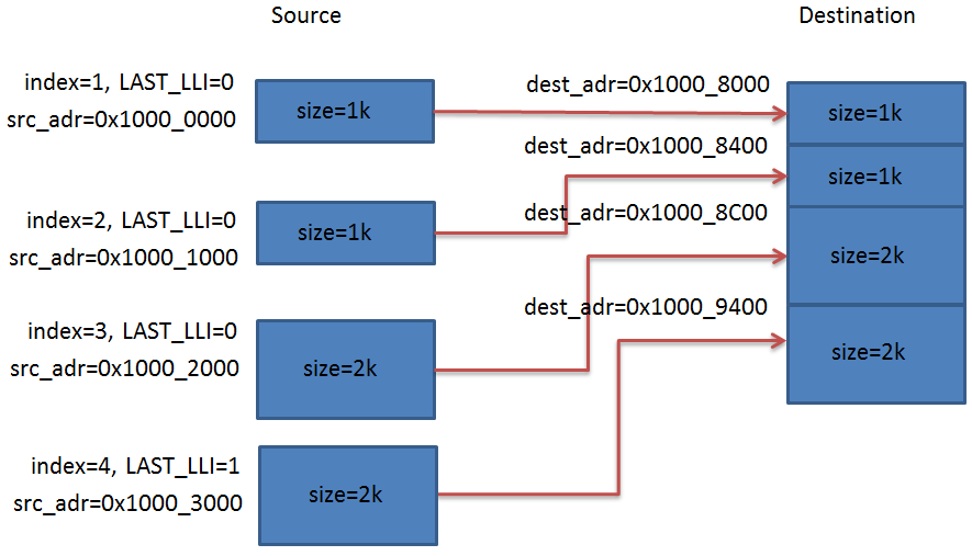
Figure 25-5 SG DMA with DMA copy mode
25.4 CBDMA Interrupts
The CBDMA interrupt events are connected to the same interrupt vector, please refer to Group 26.5 register. These events generate an interrupt if the corresponding "Enable Control Bit" is set, please refer to Group 26.6 register.
25.5 Registers Map
25.5.1 Registers Memory Map
Address | Group No. | Register Name | Register Description |
0x9C000D00 | G26.0 | CBDMA_HW_VERSION | HW Version Register |
0x9C000D04 | G26.1 | CBDMA_CONFIG | Configure CBDMA mode Register |
0x9C000D08 | G26.2 | CBDMA_LENGTH | Set CBDMA Transfer Length Register |
0x9C000D0C | G26.3 | CBDMA_SRC_ADDR | CBDMA Source Address Register |
0x9C000D10 | G26.4 | CBDMA_DES_ADDR | CBDMA Destination Address Register |
0x9C000D14 | G26.5 | CBDMA_INT_FLAG | CBDMA Interrupt Flag |
0x9C000D18 | G26.6 | CBDMA_INT_ENABLE | CBDMA Interrupt Enable |
0x9C000D1C | G26.7 | CBDMA_MEMSET_VALUE | MEMSET Value Register |
0x9C000D20 | G26.8 | CBDMA_SDRAM_SIZE_CFG | SDRAM A/B size Configuration |
0x9C000D24 | G26.9 | CBDMA_ILLEGLE_RECORD | CBDMA Illegal Access Record |
0x9C000D28 | G26.10 | SG_CBDMA_INDEX | SG_CBDMA_INDEX Setting |
0x9C000D2C | G26.11 | SG_CBDMA_CONFIG | SG_CBDMA_CONFIG Setting |
0x9C000D30 | G26.12 | SG_CBDMA_LENGTH | SG_CBDMA_LENGTH Setting |
0x9C000D34 | G26.13 | SG_CBDMA_SRC_ADDR | SG_CBDMA_SRC_ADDR Setting |
0x9C000D38 | G26.14 | SG_CBDMA_DES_ADDR | SG_CBDMA_DES_ADDR Setting |
0x9C000D3C | G26.15 | SG_CBDMA_MEMSET_VALUE | SG_CBDMA_MEMSET_VALUE Setting |
0x9C000D40 | G26.16 | SG_CBDMA_SETTING | SG_SETTING for SG_DMA_ENABLE and SG_DMA_GO |
0x9C000D44 | G26.17 | SG_LOOP_MODE_SETTING | SG_LOOP_SRAM_START Setting |
0x9C000D48 | G26.18 | SG_LOOP_SRAM_START | SG_LOOP_SRAM_SIZE Setting |
0x9C000D4C | G26.19 | SG_LOOP_SRAM_SIZE | SG_LOOP_SRAM_SIZE Setting |
0x9C000D50 | G26.20 | CBDMA_CHECK_MODE | CBDMA_CHECK_MODE Setting |
0x9C000D54 | G26.21 | CBDMA_CHECK_SUM_RESULT | CBDMA_CHECK_SUM_RESULT |
0x9C000D58 | G26.22 | CBDMA_CHECK_XOR_RESULT | CBDMA_CHECK_XOR_RESULT |
25.5.2 Registers Description
RGST Table Group 26 CB DMA: CBUS DMA Controller
26.0 DMA HW VER (dma hw ver)
Address: 0x9C000D00
Reset: 0x1751300
Field Name | Bit | Access | Description |
| DMA HW VER | 31:0 | RO | Hardware Version A constant, usually stands for h/w delivery date, such as 32'h20150803 |
26.1 DMA CONFIG (dma config)
Address: 0x9C000D04
Reset: 0x80030000
Field Name | Bit | Access | Description |
| DMA TOUCH PROT SRAM | 31 | RW | DMA TOUCH PROT SRAM 0 : if normal access touch the prot sram, the HW will fix the ADDR and LEN make this access in normal range. 1 : if normal access touch the prot sram, DMA has no any modify, only trig- ger DMA DONE and Interrupt. |
| Reserved | 30:18 | RO | RESERVED |
| CMD QUE DEPTH | 17:16 | RW | Set MEMSET Send CMD Queue Depth 0x0: depth = 1; 0x1: depth = 2; 0x2: depth = 4; 0x3: depth = 8 (default); |
| Reserved | 15:9 | RO | RESERVED |
| DMA GO | 8 | RU | DMA GO Signal Write 1 to trigger DMA hardware, self clear to zero when current operation has been finished. |
| Reserved | 7:2 | RO | RESERVED |
| DMA MODE | 1:0 | RW | Set DMA Mode 0x0: MEMSET (memset value to main memory) (default) 0x1: DMA WRITE (write data from internal SRAM to main memory) 0x2: DMA READ (read data from main memory to internal SRAM) 0x3: DMA COPY (read data from main memory then write to other space of main memory) |
26.2 DMA LENGTH (dma length)
Address: 0x9C000D08
Reset: 0x00000000
Field Name | Bit | Access | Description |
| Reserved | 31:25 | RO | RESERVED |
| DMA LENGTH | 24:0 | RW | Set DMA Length DMA read and write function support length from 1bytes to 64Kbytes. Valid when DMA GO is set to 1, and can not be changed when DMA GO assert. |
26.3 DMA SRC ADR (dma src adr)
Address: 0x9C000D0C
Reset: 0x00000000
Field Name | Bit | Access | Description |
Reserved | 31 | RO | RESERVED |
| DMA SRC ADR | 30:0 | RW | DMA Source Address • MEMSET: indicate the byte offset of memset value, only [1:0] valid. • DMA WRITE: indicate SRAM address,range 0x0000 0000 ∼ 0x0001 ffff, • DMA READ: indicate DRAM address, MBUS0's range 0x0000 0000 ∼ 0x0fff ffff, • DMA COPY: indicate DRAM address, MBUS0's range 0x0000 0000 ∼ 0x0fff ffff, Valid when DMA GO is set to 1, and can not be changed when DMA GO assert. |
26.4 DMA DES ADR (dma des adr)
Address: 0x9C000D10
Reset: 0x00000000
Field Name | Bit | Access | Description |
| Reserved | 31 | RO | RESERVED |
| DMA DES ADR | 30:0 | RW | DMA Destination Address • MEMSET: indicate DRAM address, MBUS0's range 0x0000 0000 ∼ 0x0fff ffff, • DMA WRITE: indicate DRAM address, MBUS0's range 0x0000 0000 ∼ 0x0fff ffff, • DMA READ:indicate SRAMaddress,range 0x0000 0000 ∼ 0x0001 ffff • DMA COPY: indicate DRAM address, MBUS0's range 0x0000 0000 ∼ 0x0fff ffff, Valid when DMA GO is set to 1, and can not be changed when DMA GO assert. |
26.5 DMA INT FLAG (dma int flag)
Address: 0x9C000D14
Reset: 0x00000000
Field Name | Bit | Access | Description |
Reserved | 31:7 | RO | RESERVED |
COPY ADDR OVLAP | 6 | W1C | DMA Copy Address Overlap DMA copy DMA SRC ADR and DMA DES ADR overlap and DMA DES ADR>DMA SRC ADR, DMA DES ADR<(DMA SRC ADR+DMA LENGTH) will assert this flag. Write 1 clear. |
DMA SDRAMB OVFLOW | 5 | W1C | DMA Access SDRAM-B Overflow The DMA access address out of range of the SDRAM-B will assert this flag, write 1 clear. DMA read or copy, DMA SRC ADDR+DMA LENGTH>1G+SDR B size; DMA write, copy or memset |
DMA SDRAMA OVFLOW | 4 | W1C | DMA Access SDRAM-A Overflow The DMA access address out of range of the SDRAM-A will assert this flag, write 1 clear. DMA read or copy, DMA SRC ADDR+DMA LENGTH>SDRAM-A size; DMA write, copy or memset |
DMA SRAM OVFLOW | 3 | W1C | DMA Access SRAM Over Flow The DMA access address out of the range of 0∼64K will assert this flag. Write 1 clear.DMA read, the DES ADDR+DMA LENGTH>64K; DMA write the SRC ADDR+DMA LENGTH>64K. |
CBSRAM OVFLOW | 2 | W1C | CBSRAM Over Flow The CBUS access address out of the 0∼64KBytes will assert this flag, write 1 clear. —CB DMA ADDR[15:13]=1 or (CB DMA ADDR[12:3]+CB DMA BURST LEN)>8K. |
| ADDR CONFLICT | 1 | W1C | Address Conflict If CBUS access the highest 256Bytes in CBSRAM when DMA copy will assert this flag, write 1 clear |
| DMA DONE FLAG | 0 | W1C | DMA Done If DMA done will assert this flag, write 1 clear |
26.6 DMA INT EN (dma int en)
Address: 0x9C000D18
Reset: 0x00000001
Field Name | Bit | Access | Description |
| Reserved | 31:10 | RO | RESERVED |
| LENGTH0 INT EN | 9 | RW | DMA setting for length0 Interrupt Enable Write 1 to enable DMA length0 interrupt function. |
| ACCESS PROT RANGE EN | 8 | RW | DMA access Prot Range complete Interrupt Enable Write 1 to enable DMA access Prot Range complete interrupt function. |
| LOOP SRAM OVFLOW EN | 7 | RW | DMA Loop sram address Overlap Interrupt Enable Write 1 to enable Loop Sram Address overlap interrupt function. |
| COPY ADDR OVLAP EN | 6 | RW | DMA Copy Address Overlap Interrupt Enable Write 1 to enable DMA copy DMA SRC ADDR and DMA DES ADR overlap interrupt function. |
| DMA SDRAMB OVFLOW EN | 5 | RW | DMA Access SDRAM-B Over Flow Interrupt Enable Write 1 to enable DMA SDRAMB OVFLOW interrupt function. |
| DMA SDRAMA OVFLOW EN | 4 | RW | DMA Access SDRAM-A Over Flow Interrupt Enable Write 1 to enable DMA SDRAMA OVFLOW interrupt function. |
| DMA SRAM OVFLOW EN | 3 | RW | DMA Access SRAM Over Flow Interrupt Enable Write 1 to enable DMA SRAM OVFLOW interrupt function. |
| CBSRAM OVFLOW EN | 2 | RW | CBSRAM Over Flow Interrupt Enable Write 1 to enable CBSRAM OVFLOW interrupt function |
| RSV0 | 1 | RO | Reserved bits not used |
| DMA DONE EN | 0 | RW | DMA Done Interrupt Enable Write 1 to enable DMA DONE interrupt function, default is enable |
26.7 MEMSET VALUE (memset value)
Address: 0x9C000D1C
Reset: 0x0000000
Field Name | Bit | Access | Description |
MEMSET VALUE | 31:0 | RW | MEMSET Value |
26.8 (Reserve)
Address: 0x9C000D20
Reset: 0x00000000
Field Name | Bit | Access | Description |
RSV | 31:0 | RUW | RESERVED |
26.9 (Reserve)
Address: 0x9C000D24
Reset: 0x00000000
Field Name | Bit | Access | Description |
RSV | 31:0 | RUW | RESERVED |
26.10 SG (Scatter-Gather) DMA INDEX (sg dma index)
Address: 0x9C000D28
Reset: 0x00000000
Field Name | Bit | Access | Description |
| Reserved | 31:13 | RO | RESERVED |
| SG LLI RUN INDEX | 12:8 | RW | The start LLI (Link List Item) index in a task If the task stop cause error occur, SG LLI RUN INDEX will indicate which LLI fail. |
| Reserved | 7:5 | RO | RESERVED |
| SG LLI ACCESS INDEX | 4:0 | RW | Index for LLI (Link List Item) access Determine which LLI mapping to registers G26.11~15 |
26.11 SG DMA CONFIG (sg dma config)
Address: 0x9C000D2C
Reset: 0x00000000
Field Name | Bit | Access | Description |
| Reserved | 31:3 | RO | RESERVED |
| SG LAST LLI IN TASK | 2 | RW | Last LLI (Link List Item) in a task flag for LLI 0:when this LLI finish, execute next LLI (default) 1:when this LLI finish, SGDMA stop |
| DMA MODE | 1:0 | RW | Set DMA Mode for LLI (Link List Item) 0x0: MEMSET (memset value to main memory) (default) 0x1: DMA WRITE (write data from internal SRAM to main memory) 0x2: DMA READ (read data from main memory to internal SRAM) 0x3: DMA COPY (read data from main memory then write to other space of main memory) |
26.12 SG DMA LENGTH (sg dma length)
Address: 0x9C000D30
Reset: 0x00000000
Field Name | Bit | Access | Description |
| SG DMA LENGTH | 31:0 | RUW | Set DMA Length for LLI (Link List Item) DMA read and write function support length from 1bytes to 64Kbytes. Valid when DMA GO is set to 1, and can not be changed when DMA GO assert. read from SRAM that bit number is 32, but the currently bit number is 25 |
26.13 SG DMA SRC ADR (sg dma src adr)
Address: 0x9C000D34
Reset: 0x00000000
Field Name | Bit | Access | Description |
Reserved | 31 | RUW | RESERVED |
SG DMA SRC ADR | 30:0 | RUW | DMA Source Address for LLI (Link List Item) • MEMSET: indicate the byte offset of memset value, only [1:0] valid. |
26.14 SG DMA DES ADR (sg dma des adr)
Address: 0x9C000D38
Reset: 0x00000000
Field Name | Bit | Access | Description |
Reserved | 31 | RUW | RESERVED |
| SG DMA DES ADR | 30:0 | RUW | DMA Destination Address for LLI (Link List Item) • MEMSET: indicate DRAM address, MBUS0's range 0x0000 0000 ∼ 0x0fff ffff, • DMA WRITE: indicate DRAM address, MBUS0's range 0x0000 0000 ∼ 0x0fff ffff, • DMA READ:indicate SRAMaddress,range 0x0000 0000 ∼ 0x0001 ffff • DMA COPY: indicate DRAM address, MBUS0's range 0x0000 0000 ∼ 0x0fff ffff, Valid when DMA GO is set to 1, and can not be changed when DMA GO assert. |
26.15 SG MEMSET VALUE (sg memset value)
Address: 0x9C000D3C
Reset: 0x00000000
Field Name | Bit | Access | Description |
SG MEMSET VALUE | 31:0 | RUW | MEMSET Value for LLI (Link List Item) |
26.16 SG SETTING (sg setting)
Address: 0x9C000D40
Reset: 0x00000000
Field Name | Bit | Access | Description |
| SG DMA ENABLE | 31 | RW | SG(Scatter-gather) function enable 0:Disable SG(Scatter-gather) function (default) 1:Enable SG(Scatter-gather) function |
| Reserved | 30:1 | RO | RESERVED |
| SG DMA GO | 0 | RUW | DMA GO Signal for LLI (Link List Item) Write 1 to trigger SG DMA hardware, self clear to zero when task finish or task stop cause error occur. |
26.17 SG LOOP MODE SETTING (sg loop mode setting)
Address: 0x9C000D44
Reset: 0x00000000
Field Name | Bit | Access | Description |
| Reserved | 31:1 | RO | RESERVED |
| SG LOOP MODE SETTING | 0 | RW | DMA loop mode for LLI (Link List Item) Write 1 to trigger SG DMA loop mode that will be ignore the DMA mode and let the SRC/DES ADDR on DRAM addr. |
26.18 SG LOOP SRAM START (sg loop sram start)
Address: 0x9C000D48
Reset: 0x00000000
Field Name | Bit | Access | Description |
| SG LOOP SRAM START | 31:0 | RUW | DMA start addr for loop mode for LLI (Link List Item) you can setting the start addr to call the DMA access on SRAM |
26.19 SG LOOP SRAM SIZE (sg loop sram size)
Address: 0x9C000D4C
Reset: 0x00000005
Field Name | Bit | Access | Description |
| Reserved | 31:4 | RO | RESERVED |
SG LOOP SRAM SIZE | 3:0 | RW | loop mode access SRAM's size for LLI (Link List Item) if you setting the loop start addr the judge SRAM size to use for LLI 0x0 : 1KB 0x1 : 2KB 0x2 : 4KB 0x3 : 8KB 0x4 : 16KB 0x5 : 32KB (default) 0x6 : 64KB other reserved. the maximum size is according to SRAM size. |
26.20 CBDMA CHECK MODE (cbdma check mode)
Address: 0x9C000D50
Reset: 0x00000000
Field Name | Bit | Access | Description |
| DRAM SRAM CHECK MAPPING | 31 | RW | DRAM SRAM check mapping in CBDMA access, DRAM to SRAM will shift data by SRC ADR and DES ADR. if SRC ADR[1:0] != DES ADR[1:0], the result will be different. 0 : CBDMA check xor result not match to DRAM. 1 : CBDMA check xor result need to match to DRAM. |
| Reserved | 30:2 | RO | RESERVED |
| CBDMA CHECK RD ONLY | 1 | RW | CBDMA CHECK RD ONLY in check sum mode, rdata will be check for CBDMA access. but wdata can't send to BUS. |
| CBDMA CHECK NORMAL | 0 | RW | CBDMA CHECK NORMAL in check sum mode, rdata will be check for CBDMA access. |
26.21 CBDMA CHECK SUM RESULT (cbdma check sum result)
Address: 0x9C000D54
Reset: 0x00000000
Field Name | Bit | Access | Description |
CBDMA CHECK SUM RESULT | 31:0 | RO | check the sum result if you have been set the check sum/xor mode, you can read this register for check sum when CBDMA access done. |
26.22 CBDMA CHECK XOR RESULT (cbdma check xor result)
Address: 0x9C000D58
Reset: 0x00000000
Field Name | Bit | Access | Description |
| CBDMA CHECK XOR RESULT | 31:0 | RO | check the xor result if you have been set the check sum/xor mode, you can read this register for check xor when CBDMA access done. |